EP0183060A2 - Process for the photoselective metallization on non-conductive plastic base materials - Google Patents
Process for the photoselective metallization on non-conductive plastic base materials Download PDFInfo
- Publication number
- EP0183060A2 EP0183060A2 EP85113563A EP85113563A EP0183060A2 EP 0183060 A2 EP0183060 A2 EP 0183060A2 EP 85113563 A EP85113563 A EP 85113563A EP 85113563 A EP85113563 A EP 85113563A EP 0183060 A2 EP0183060 A2 EP 0183060A2
- Authority
- EP
- European Patent Office
- Prior art keywords
- solvent
- metal
- substrate
- pattern
- metal pattern
- Prior art date
- Legal status (The legal status is an assumption and is not a legal conclusion. Google has not performed a legal analysis and makes no representation as to the accuracy of the status listed.)
- Granted
Links
Images


Classifications
-
- C—CHEMISTRY; METALLURGY
- C23—COATING METALLIC MATERIAL; COATING MATERIAL WITH METALLIC MATERIAL; CHEMICAL SURFACE TREATMENT; DIFFUSION TREATMENT OF METALLIC MATERIAL; COATING BY VACUUM EVAPORATION, BY SPUTTERING, BY ION IMPLANTATION OR BY CHEMICAL VAPOUR DEPOSITION, IN GENERAL; INHIBITING CORROSION OF METALLIC MATERIAL OR INCRUSTATION IN GENERAL
- C23C—COATING METALLIC MATERIAL; COATING MATERIAL WITH METALLIC MATERIAL; SURFACE TREATMENT OF METALLIC MATERIAL BY DIFFUSION INTO THE SURFACE, BY CHEMICAL CONVERSION OR SUBSTITUTION; COATING BY VACUUM EVAPORATION, BY SPUTTERING, BY ION IMPLANTATION OR BY CHEMICAL VAPOUR DEPOSITION, IN GENERAL
- C23C18/00—Chemical coating by decomposition of either liquid compounds or solutions of the coating forming compounds, without leaving reaction products of surface material in the coating; Contact plating
- C23C18/16—Chemical coating by decomposition of either liquid compounds or solutions of the coating forming compounds, without leaving reaction products of surface material in the coating; Contact plating by reduction or substitution, e.g. electroless plating
- C23C18/1601—Process or apparatus
- C23C18/1603—Process or apparatus coating on selected surface areas
- C23C18/1607—Process or apparatus coating on selected surface areas by direct patterning
- C23C18/1608—Process or apparatus coating on selected surface areas by direct patterning from pretreatment step, i.e. selective pre-treatment
-
- H—ELECTRICITY
- H05—ELECTRIC TECHNIQUES NOT OTHERWISE PROVIDED FOR
- H05K—PRINTED CIRCUITS; CASINGS OR CONSTRUCTIONAL DETAILS OF ELECTRIC APPARATUS; MANUFACTURE OF ASSEMBLAGES OF ELECTRICAL COMPONENTS
- H05K1/00—Printed circuits
- H05K1/18—Printed circuits structurally associated with non-printed electric components
-
- C—CHEMISTRY; METALLURGY
- C23—COATING METALLIC MATERIAL; COATING MATERIAL WITH METALLIC MATERIAL; CHEMICAL SURFACE TREATMENT; DIFFUSION TREATMENT OF METALLIC MATERIAL; COATING BY VACUUM EVAPORATION, BY SPUTTERING, BY ION IMPLANTATION OR BY CHEMICAL VAPOUR DEPOSITION, IN GENERAL; INHIBITING CORROSION OF METALLIC MATERIAL OR INCRUSTATION IN GENERAL
- C23C—COATING METALLIC MATERIAL; COATING MATERIAL WITH METALLIC MATERIAL; SURFACE TREATMENT OF METALLIC MATERIAL BY DIFFUSION INTO THE SURFACE, BY CHEMICAL CONVERSION OR SUBSTITUTION; COATING BY VACUUM EVAPORATION, BY SPUTTERING, BY ION IMPLANTATION OR BY CHEMICAL VAPOUR DEPOSITION, IN GENERAL
- C23C18/00—Chemical coating by decomposition of either liquid compounds or solutions of the coating forming compounds, without leaving reaction products of surface material in the coating; Contact plating
- C23C18/16—Chemical coating by decomposition of either liquid compounds or solutions of the coating forming compounds, without leaving reaction products of surface material in the coating; Contact plating by reduction or substitution, e.g. electroless plating
- C23C18/1601—Process or apparatus
- C23C18/1603—Process or apparatus coating on selected surface areas
- C23C18/1607—Process or apparatus coating on selected surface areas by direct patterning
- C23C18/1612—Process or apparatus coating on selected surface areas by direct patterning through irradiation means
-
- C—CHEMISTRY; METALLURGY
- C23—COATING METALLIC MATERIAL; COATING MATERIAL WITH METALLIC MATERIAL; CHEMICAL SURFACE TREATMENT; DIFFUSION TREATMENT OF METALLIC MATERIAL; COATING BY VACUUM EVAPORATION, BY SPUTTERING, BY ION IMPLANTATION OR BY CHEMICAL VAPOUR DEPOSITION, IN GENERAL; INHIBITING CORROSION OF METALLIC MATERIAL OR INCRUSTATION IN GENERAL
- C23C—COATING METALLIC MATERIAL; COATING MATERIAL WITH METALLIC MATERIAL; SURFACE TREATMENT OF METALLIC MATERIAL BY DIFFUSION INTO THE SURFACE, BY CHEMICAL CONVERSION OR SUBSTITUTION; COATING BY VACUUM EVAPORATION, BY SPUTTERING, BY ION IMPLANTATION OR BY CHEMICAL VAPOUR DEPOSITION, IN GENERAL
- C23C18/00—Chemical coating by decomposition of either liquid compounds or solutions of the coating forming compounds, without leaving reaction products of surface material in the coating; Contact plating
- C23C18/16—Chemical coating by decomposition of either liquid compounds or solutions of the coating forming compounds, without leaving reaction products of surface material in the coating; Contact plating by reduction or substitution, e.g. electroless plating
- C23C18/18—Pretreatment of the material to be coated
- C23C18/20—Pretreatment of the material to be coated of organic surfaces, e.g. resins
- C23C18/2006—Pretreatment of the material to be coated of organic surfaces, e.g. resins by other methods than those of C23C18/22 - C23C18/30
- C23C18/2026—Pretreatment of the material to be coated of organic surfaces, e.g. resins by other methods than those of C23C18/22 - C23C18/30 by radiant energy
- C23C18/204—Radiation, e.g. UV, laser
-
- C—CHEMISTRY; METALLURGY
- C23—COATING METALLIC MATERIAL; COATING MATERIAL WITH METALLIC MATERIAL; CHEMICAL SURFACE TREATMENT; DIFFUSION TREATMENT OF METALLIC MATERIAL; COATING BY VACUUM EVAPORATION, BY SPUTTERING, BY ION IMPLANTATION OR BY CHEMICAL VAPOUR DEPOSITION, IN GENERAL; INHIBITING CORROSION OF METALLIC MATERIAL OR INCRUSTATION IN GENERAL
- C23C—COATING METALLIC MATERIAL; COATING MATERIAL WITH METALLIC MATERIAL; SURFACE TREATMENT OF METALLIC MATERIAL BY DIFFUSION INTO THE SURFACE, BY CHEMICAL CONVERSION OR SUBSTITUTION; COATING BY VACUUM EVAPORATION, BY SPUTTERING, BY ION IMPLANTATION OR BY CHEMICAL VAPOUR DEPOSITION, IN GENERAL
- C23C18/00—Chemical coating by decomposition of either liquid compounds or solutions of the coating forming compounds, without leaving reaction products of surface material in the coating; Contact plating
- C23C18/16—Chemical coating by decomposition of either liquid compounds or solutions of the coating forming compounds, without leaving reaction products of surface material in the coating; Contact plating by reduction or substitution, e.g. electroless plating
- C23C18/18—Pretreatment of the material to be coated
- C23C18/20—Pretreatment of the material to be coated of organic surfaces, e.g. resins
- C23C18/2006—Pretreatment of the material to be coated of organic surfaces, e.g. resins by other methods than those of C23C18/22 - C23C18/30
- C23C18/2046—Pretreatment of the material to be coated of organic surfaces, e.g. resins by other methods than those of C23C18/22 - C23C18/30 by chemical pretreatment
- C23C18/2053—Pretreatment of the material to be coated of organic surfaces, e.g. resins by other methods than those of C23C18/22 - C23C18/30 by chemical pretreatment only one step pretreatment
- C23C18/206—Use of metal other than noble metals and tin, e.g. activation, sensitisation with metals
-
- C—CHEMISTRY; METALLURGY
- C23—COATING METALLIC MATERIAL; COATING MATERIAL WITH METALLIC MATERIAL; CHEMICAL SURFACE TREATMENT; DIFFUSION TREATMENT OF METALLIC MATERIAL; COATING BY VACUUM EVAPORATION, BY SPUTTERING, BY ION IMPLANTATION OR BY CHEMICAL VAPOUR DEPOSITION, IN GENERAL; INHIBITING CORROSION OF METALLIC MATERIAL OR INCRUSTATION IN GENERAL
- C23C—COATING METALLIC MATERIAL; COATING MATERIAL WITH METALLIC MATERIAL; SURFACE TREATMENT OF METALLIC MATERIAL BY DIFFUSION INTO THE SURFACE, BY CHEMICAL CONVERSION OR SUBSTITUTION; COATING BY VACUUM EVAPORATION, BY SPUTTERING, BY ION IMPLANTATION OR BY CHEMICAL VAPOUR DEPOSITION, IN GENERAL
- C23C18/00—Chemical coating by decomposition of either liquid compounds or solutions of the coating forming compounds, without leaving reaction products of surface material in the coating; Contact plating
- C23C18/16—Chemical coating by decomposition of either liquid compounds or solutions of the coating forming compounds, without leaving reaction products of surface material in the coating; Contact plating by reduction or substitution, e.g. electroless plating
- C23C18/18—Pretreatment of the material to be coated
- C23C18/20—Pretreatment of the material to be coated of organic surfaces, e.g. resins
- C23C18/2006—Pretreatment of the material to be coated of organic surfaces, e.g. resins by other methods than those of C23C18/22 - C23C18/30
- C23C18/2046—Pretreatment of the material to be coated of organic surfaces, e.g. resins by other methods than those of C23C18/22 - C23C18/30 by chemical pretreatment
- C23C18/2073—Multistep pretreatment
- C23C18/208—Multistep pretreatment with use of metal first
-
- C—CHEMISTRY; METALLURGY
- C23—COATING METALLIC MATERIAL; COATING MATERIAL WITH METALLIC MATERIAL; CHEMICAL SURFACE TREATMENT; DIFFUSION TREATMENT OF METALLIC MATERIAL; COATING BY VACUUM EVAPORATION, BY SPUTTERING, BY ION IMPLANTATION OR BY CHEMICAL VAPOUR DEPOSITION, IN GENERAL; INHIBITING CORROSION OF METALLIC MATERIAL OR INCRUSTATION IN GENERAL
- C23C—COATING METALLIC MATERIAL; COATING MATERIAL WITH METALLIC MATERIAL; SURFACE TREATMENT OF METALLIC MATERIAL BY DIFFUSION INTO THE SURFACE, BY CHEMICAL CONVERSION OR SUBSTITUTION; COATING BY VACUUM EVAPORATION, BY SPUTTERING, BY ION IMPLANTATION OR BY CHEMICAL VAPOUR DEPOSITION, IN GENERAL
- C23C18/00—Chemical coating by decomposition of either liquid compounds or solutions of the coating forming compounds, without leaving reaction products of surface material in the coating; Contact plating
- C23C18/16—Chemical coating by decomposition of either liquid compounds or solutions of the coating forming compounds, without leaving reaction products of surface material in the coating; Contact plating by reduction or substitution, e.g. electroless plating
- C23C18/18—Pretreatment of the material to be coated
- C23C18/20—Pretreatment of the material to be coated of organic surfaces, e.g. resins
- C23C18/22—Roughening, e.g. by etching
- C23C18/24—Roughening, e.g. by etching using acid aqueous solutions
-
- C—CHEMISTRY; METALLURGY
- C23—COATING METALLIC MATERIAL; COATING MATERIAL WITH METALLIC MATERIAL; CHEMICAL SURFACE TREATMENT; DIFFUSION TREATMENT OF METALLIC MATERIAL; COATING BY VACUUM EVAPORATION, BY SPUTTERING, BY ION IMPLANTATION OR BY CHEMICAL VAPOUR DEPOSITION, IN GENERAL; INHIBITING CORROSION OF METALLIC MATERIAL OR INCRUSTATION IN GENERAL
- C23C—COATING METALLIC MATERIAL; COATING MATERIAL WITH METALLIC MATERIAL; SURFACE TREATMENT OF METALLIC MATERIAL BY DIFFUSION INTO THE SURFACE, BY CHEMICAL CONVERSION OR SUBSTITUTION; COATING BY VACUUM EVAPORATION, BY SPUTTERING, BY ION IMPLANTATION OR BY CHEMICAL VAPOUR DEPOSITION, IN GENERAL
- C23C18/00—Chemical coating by decomposition of either liquid compounds or solutions of the coating forming compounds, without leaving reaction products of surface material in the coating; Contact plating
- C23C18/16—Chemical coating by decomposition of either liquid compounds or solutions of the coating forming compounds, without leaving reaction products of surface material in the coating; Contact plating by reduction or substitution, e.g. electroless plating
- C23C18/31—Coating with metals
- C23C18/32—Coating with nickel, cobalt or mixtures thereof with phosphorus or boron
- C23C18/34—Coating with nickel, cobalt or mixtures thereof with phosphorus or boron using reducing agents
- C23C18/36—Coating with nickel, cobalt or mixtures thereof with phosphorus or boron using reducing agents using hypophosphites
-
- C—CHEMISTRY; METALLURGY
- C23—COATING METALLIC MATERIAL; COATING MATERIAL WITH METALLIC MATERIAL; CHEMICAL SURFACE TREATMENT; DIFFUSION TREATMENT OF METALLIC MATERIAL; COATING BY VACUUM EVAPORATION, BY SPUTTERING, BY ION IMPLANTATION OR BY CHEMICAL VAPOUR DEPOSITION, IN GENERAL; INHIBITING CORROSION OF METALLIC MATERIAL OR INCRUSTATION IN GENERAL
- C23C—COATING METALLIC MATERIAL; COATING MATERIAL WITH METALLIC MATERIAL; SURFACE TREATMENT OF METALLIC MATERIAL BY DIFFUSION INTO THE SURFACE, BY CHEMICAL CONVERSION OR SUBSTITUTION; COATING BY VACUUM EVAPORATION, BY SPUTTERING, BY ION IMPLANTATION OR BY CHEMICAL VAPOUR DEPOSITION, IN GENERAL
- C23C18/00—Chemical coating by decomposition of either liquid compounds or solutions of the coating forming compounds, without leaving reaction products of surface material in the coating; Contact plating
- C23C18/16—Chemical coating by decomposition of either liquid compounds or solutions of the coating forming compounds, without leaving reaction products of surface material in the coating; Contact plating by reduction or substitution, e.g. electroless plating
- C23C18/31—Coating with metals
- C23C18/38—Coating with copper
- C23C18/40—Coating with copper using reducing agents
- C23C18/405—Formaldehyde
-
- C—CHEMISTRY; METALLURGY
- C23—COATING METALLIC MATERIAL; COATING MATERIAL WITH METALLIC MATERIAL; CHEMICAL SURFACE TREATMENT; DIFFUSION TREATMENT OF METALLIC MATERIAL; COATING BY VACUUM EVAPORATION, BY SPUTTERING, BY ION IMPLANTATION OR BY CHEMICAL VAPOUR DEPOSITION, IN GENERAL; INHIBITING CORROSION OF METALLIC MATERIAL OR INCRUSTATION IN GENERAL
- C23C—COATING METALLIC MATERIAL; COATING MATERIAL WITH METALLIC MATERIAL; SURFACE TREATMENT OF METALLIC MATERIAL BY DIFFUSION INTO THE SURFACE, BY CHEMICAL CONVERSION OR SUBSTITUTION; COATING BY VACUUM EVAPORATION, BY SPUTTERING, BY ION IMPLANTATION OR BY CHEMICAL VAPOUR DEPOSITION, IN GENERAL
- C23C18/00—Chemical coating by decomposition of either liquid compounds or solutions of the coating forming compounds, without leaving reaction products of surface material in the coating; Contact plating
- C23C18/16—Chemical coating by decomposition of either liquid compounds or solutions of the coating forming compounds, without leaving reaction products of surface material in the coating; Contact plating by reduction or substitution, e.g. electroless plating
- C23C18/31—Coating with metals
- C23C18/42—Coating with noble metals
- C23C18/44—Coating with noble metals using reducing agents
-
- H—ELECTRICITY
- H05—ELECTRIC TECHNIQUES NOT OTHERWISE PROVIDED FOR
- H05K—PRINTED CIRCUITS; CASINGS OR CONSTRUCTIONAL DETAILS OF ELECTRIC APPARATUS; MANUFACTURE OF ASSEMBLAGES OF ELECTRICAL COMPONENTS
- H05K3/00—Apparatus or processes for manufacturing printed circuits
- H05K3/10—Apparatus or processes for manufacturing printed circuits in which conductive material is applied to the insulating support in such a manner as to form the desired conductive pattern
- H05K3/18—Apparatus or processes for manufacturing printed circuits in which conductive material is applied to the insulating support in such a manner as to form the desired conductive pattern using precipitation techniques to apply the conductive material
- H05K3/181—Apparatus or processes for manufacturing printed circuits in which conductive material is applied to the insulating support in such a manner as to form the desired conductive pattern using precipitation techniques to apply the conductive material by electroless plating
- H05K3/182—Apparatus or processes for manufacturing printed circuits in which conductive material is applied to the insulating support in such a manner as to form the desired conductive pattern using precipitation techniques to apply the conductive material by electroless plating characterised by the patterning method
- H05K3/185—Apparatus or processes for manufacturing printed circuits in which conductive material is applied to the insulating support in such a manner as to form the desired conductive pattern using precipitation techniques to apply the conductive material by electroless plating characterised by the patterning method by making a catalytic pattern by photo-imaging
-
- B—PERFORMING OPERATIONS; TRANSPORTING
- B29—WORKING OF PLASTICS; WORKING OF SUBSTANCES IN A PLASTIC STATE IN GENERAL
- B29C—SHAPING OR JOINING OF PLASTICS; SHAPING OF MATERIAL IN A PLASTIC STATE, NOT OTHERWISE PROVIDED FOR; AFTER-TREATMENT OF THE SHAPED PRODUCTS, e.g. REPAIRING
- B29C35/00—Heating, cooling or curing, e.g. crosslinking or vulcanising; Apparatus therefor
- B29C35/02—Heating or curing, e.g. crosslinking or vulcanizing during moulding, e.g. in a mould
- B29C35/08—Heating or curing, e.g. crosslinking or vulcanizing during moulding, e.g. in a mould by wave energy or particle radiation
- B29C35/0805—Heating or curing, e.g. crosslinking or vulcanizing during moulding, e.g. in a mould by wave energy or particle radiation using electromagnetic radiation
- B29C2035/0855—Heating or curing, e.g. crosslinking or vulcanizing during moulding, e.g. in a mould by wave energy or particle radiation using electromagnetic radiation using microwave
Definitions
- This invention relates to photoselective metallization of non-conductive plastic base materials. More specifically, it relates to the manufacture of additive printed circuits by electrolessly platin q catalytic images on adhesion promoted surfaces of insulating base materials.
- resist imaging In one kind of fully additive processes, herein also referred to as "resist imaging" process, which is commonly employed today for producing printed circuits on resinous insulating base materials, a conductor pattern is formed by electrolessly depositing metal on an adhesion promoted surface of the resinous insulating base material. A plating resist is applied before or after adhesion promotion, onto the background, which is the area free of electrolessly deposited conductors on the finished printed circuit board.
- the surface of the insulating base material is rendered microporous and hydrophilic. This may be accomplished by plasma or by mechanical means, but is usually achieved by a strong acid or oxidizing solution, or by swelling the surface with a solvent, and then subjecting the pretreated surface to a strong oxidizing agent such as chromic acid.
- the background area is hydrophobic during electroless plating because the surface of the plating resist is hydrophobic.
- resistless imaging additive processes a conductive pattern image, catalytic for electroless deposition, is formed on the uniformly adhesion promoted and thus hydrophilic surface of an insulating base material.
- Fully additive resistless imaging processes are, therefore, characterized by a hydrophilic background during electroless plating. The presence of a hydrophilic background surface during metal plating renders such background susceptible to extraneous metal plating, which is undesirable.
- resistless systems rely, instead, on heavily stabilized plating baths and/or periodic "quick etching" during the plating cycle to minimize adherence of extraneous metal deposits.
- US 3 562 005 describes a resistless imaging process wherein an adhesion promoted surface is treated with stannous chloride.
- a conductor image is produced by exposing the surface to hard UV radiation throuqh a photographic positive of the desired circuit pattern. The exposure converts the stannous moiety between the conductors to a stannic species. Subsequently, the surface is treated with palladium chloride and only the stannous moiety remaining in the conductive pattern reacts with the palladium chloride to form an image catalytic for electroless metal deposition.
- This process while capable of reproducing conductor images of very fine detail, never was used in production by the applicant because of defects caused by extraneous metal deposition.
- US 3 772 078; 3 930 963; 3 959 547; and 3 994 727 teach a resistless imaging process for producing printed circuits wherein a real image is produced on a surface of an insulating base material which has been treated with a solvent such as dimethylformamide and with chromic acid and/ or sulfuric acid to adhesion promote the surface.
- the adhesion promoted surface is treated with a solution containing copper salts, 2,6-anthraquinone disulfonic acid and a p olvol, dried and then exposed to printing light through a photographic negative to produce a real image of copper nuclei which are catalytic for electroless copper plating.
- US 4 262 085 describes another improvement to the prior art processes .
- the copper nuclei are exchanged with palladium, followed by a rinsing step and deposition of a thin coating of electroless nickel and then electroless deposition of a copper conductive pattern from a solution stabilized with potassium selenocyanate.
- Vapor Polishing with methylene chloride has been used to remove scratches from thermoplastics such as polycarbonate, leaving a smooth, glossy finish, e.g.; see “Resin LexaJID-Technifact Bulletin” (11/82) by General Electric Co. Vapor polishing also has been used to restore semi-additive printed circuits on polysulfone based material to a transparent state.
- An object of this invention is the formation of metal patterns including printed circuit conductor patterns on polymeric substrates by resistless imaging techniques without extraneous metal deposition.
- Another object is to provide a process for eliminating micropores present on the surface of an adhesion promoted thermoplastic substrate in areas not corresponding to the pattern to be formed by metal deposition; subsequent to formation of a reinforced image of the pattern on the surface by a metal plating step.
- a further object of this invention is to provide a process for rendering hydrophobic the surface of a polymeric substrate or surface coating layer in areas which do not correspond to a desired metal pattern after establishing an image of the metal pattern to be formed.
- Another object of this invention is to provide a process for eliminating micropores in the background (the areas between areas corresponding to the desired metal, e.g, conductor pattern) of fully additively plated printed circuit boards whose substrates comprise a high temperature thermoplastic polymer, in order to prevent indiscriminate metal deposition and to enhance surface electrical properties as well as aesthetic qualities of the printed circuit board.
- a still further object of this invention is to provide an improved process for manufacturing a metal core circuit board.
- Another object is to provide an improved process for producing conductor patterns on three-dimensional polymer articles.
- Still another object of this invention is to provide a process for forming metal patterns without extraneous metal deposition on thermoplastic articles having heat distortion temperatures below 170°C.
- aromatic polyether polymer is meant a thermoplastic polymer characterized bv recurrinq aromatic and ether units in the polvmer chain.
- aromatic polyether polymer include sulfone polymers, polyetherimides and polyetherketones.
- high temperature thermoplastic polymer a polymer having an aromatic backbone that does not liquefy or decompose at a temperature of about 245°C after 5 seconds exposure at such a temperature.
- the polymer has a heat deflection temperature of 170°C.
- solvate is meant the adsorption of a surface layer of solvent by a polymer, which may be accompanied by swelling of the polymer surface.
- the present invention provides a process for producing a metal pattern on a resinous surface of non-conductive substrate which includes the steps of treating the surface of said substrate to render it hydrophilic and microporous; providing the thus prepared surface with an image corresponding to the desired metal pattern and formed of sites catalytic to electroless metal deposition and depositing metal on the catalytic pattern to form the metal pattern; the process further comprising the steps of, subsequently to said electroless metal deposition, contacting the resinous surface with a solvent in which the resinous surface is at least partially soluble for a time period sufficient to permit the solvated base material to flow against and adhere to the edges of the metal pattern, but insufficient to permit the solvated resinous surface to flow onto the metal pattern; and immediately drying the solvated surface and evaporating the solvent at a temperature at which the solvent rapidly volatilizes to stop said flow, leaving the edges of the metal pattern adhered to the resinous surface at their intersection, and restoring the surface to its hydrophobic state.
- the invention further provides a process for producing a metal pattern on a non-conductive resinous substrate which includes the steps of treating the surface of said substrate to render it hydrophilic and microporous; providing the thus prepared surface with an image corresponding to the desired metal pattern and formed of sites catalytic to electroless metal deposition,
- the said process comprising exposing said surface provided with said catalytic image to a first electroless metal plating solution for a time sufficient to initiate metal deposition and to reinforce said catalytic site pattern image; restoring the non-imaged surface of the substrate by rendering it hydrophobic and resistant to electroless metal deposition by contacting the substrate with a solvent or solvent composition in which the substrate is at least partially soluble for a time period sufficient to solvate the surface of the substrate, but insufficient to result in stress cracking or flow of the substrate onto the reinforced image, and immediately drying the solvated surface of the base material at room temperature at which the solvent rapidly volatilizes to restore the hydrophobicity of the surface; and exposing the surface to a second electroless metal plating solution to deposit metal on the reinforced catalytic pattern thus forming the metal pattern, the restored hydrophobicity of the non-imaged surface areas inhibiting metal deposition thereon.
- the invention provides a process for restoring hydrophobicity to and smoothening the exposed surface of an adhesion promoted resinous surface of a base material after a catalytic resistless image has been imposed thereon.
- the base material may be comprised of a resin-rich, epoxy impregnated, glass cloth laminate, a resin coated metal core base material, a thermoplastic or thermoset polymer, or a thermoset laminate clad with a high temperature thermoplastic polymer.
- the surface of the base material Prior to imposing the resistless image, the surface of the base material is treated to render it microporous and hydrophilic, thus suitable for securely adhering electrolessly formed metal deposits. It has been found that hydrophobicity and a smooth surface can be restored to the treated and thus hydrophilic and microporous resinous surface by exposing it to a solvent or solvent vapors in which the exposed resin surface region may be solubilized for a time period sufficient to solvate the surface region but insufficient to result in stress cracking or flow of the resinous surface onto the metal pattern plated on the surface, and hereafter immediately drying the polymer at a temperature at which the solvent rapidly volatilizes thus restoring hydrophobicity of the surface and preventing flow of the resinous surface onto the metal pattern.
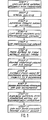
- Fig. 1 is a schematic flowchart illustrating a process for producing a printed circuit on a polymeric base material according to the present invention.
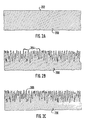
- Fig. 2A to 2I is a side view in cross section of a surface region of the polymer base material showing the surface region at stages in the formation of a printed circuit according to the process of this invention.
- the invention relates to a process for preparing a metal pattern on a resinous surface of a non-conductive substrate including the steps of treating one or more surfaces of a non-conductive substrate to render them hydrophilic and microporous by adhesion promotion, imaging a catalytic pattern corresponding to the desired metal pattern of the surface(s), and depositing metal on the catalytic pattern to form the metal pattern.
- the resinous surface(s) is (are) contacted with a solvent in which the said resinous surface(s) is (are) at least partially soluble for a time period sufficient to permit the solvated resinous surface(s) to flow against and adhere to the edges of the metal pattern, but insufficient to permit the solvated resinous surface(s) to flow onto the metal pattern, and immediately evaporating the solvent from the resinous surface(s) at a temperature at which the solvent rapidly volatilizes to stop and flow, leaving the edges of the metal pattern adhered to the resinous surface(s) at their intersection.
- One embodiment of the invention provides a process for treating the surface of a non-conductive substrate such as a polymer base material containing a metal deposit thereon.
- a non-conductive substrate such as a polymer base material containing a metal deposit thereon.
- the surface of the polymer base material has been adhesion promoted by conventional techniques prior to metal deposition, e.g., by chemical treatment with a highly oxidizing solution or with a plasma under conditions sufficient to render the surface hydrophilic.
- the hydrophilic surface provides sites for chemical and/or mechanical linking to a metal layer.
- a metal pattern may be applied to the adhesion promoted surface by conventional techniques, i.e., by imaging a pattern which is catalytic for electroless metal deposition on the surface by conventional photoforming techniques.
- the imaged pattern is then reinforced by electroless metal deposition until the metal pattern has a thickness of between 0.5 ⁇ m and 5 ⁇ m.
- the non-imaged surface areas of the base material are rendered smooth, hydrophobic and resistant to extraneous metal deposition. This may be accomplished by immersing the polymer in a solvent in which it is at least partially soluble and for a time period sufficient to solvate the polymer surface but insufficient to result in stress cracking or flow of the polymer onto the metal pattern. The time period will vary between about 1 second and about 1 minute depending on the solvent system selected and the polymer system being treated.
- the solvent systems include a strong solvent for the polymer and suitable diluents. Among the diluents are aliphatic hydrocarbons, aliphatic alcohols and water.
- the polymer surface is dried at a temperature at which the solvent
- the drying temperature is from room temperature up to about 200°C depending upon the polymer and the solvent systems used. Preferably, the drying temperature is between about room temperature and about 125°C.
- the immersion may be in a liquid solvent such as ketones, esters, aromatic or aprotic solvents, or in solvent vapors of halogenated hydrocarbons with boiling points below the heat distortion temperature of the polymer.
- a liquid solvent such as ketones, esters, aromatic or aprotic solvents, or in solvent vapors of halogenated hydrocarbons with boiling points below the heat distortion temperature of the polymer.
- Suitable non-conductive substrates include thermoset polymers such as epoxy resins, a thermoset or thermoplastic resin coated, metal core base material, thermoplastic polymers as defined hereinafter, a thermoset laminate clad with a high temperature thermoplastic polymer, or resin-rich laminates such as glass cloth reinforced epoxy-resin laminates with a significant thickness of non-reinforced surface-layer epoxy resin.
- Preferred surface layer epoxy resins include diglycidyl ethers of bisphenol A.
- Insulated metal core base materials include steel and aluminum sheets which may have been perforated with a printed circuit hole pattern and are coated with an insulating resinous material. Suitable insulating resinous materials include epoxy resin coating compositions and high temperature thermoplastic polymers as described hereinbelow.
- powder coating techniques such as powder spray coating, electrostatic powder coating and fluidized bed powder coating.
- Suitable thermoplastic polymers include high temperature thermoplastic polymers such as sulfone polymers, polyetherimides, polyphenylene sulfides and polyetherether- ketones and are believed to include low temperature thermoplastic polymers such as platable grades of polyethylene and acrylonitrile-butadiene-styrene (ABS).
- high temperature thermoplastic polymers such as sulfone polymers, polyetherimides, polyphenylene sulfides and polyetherether- ketones and are believed to include low temperature thermoplastic polymers such as platable grades of polyethylene and acrylonitrile-butadiene-styrene (ABS).
- Preferred sulfone polymers according to this invention are polysulfone and polyethersulfone.
- thermoplastic polymers in molded forms or in extruded sheets, rods and/or film forms initially have hydrophobic and translucent or transparent surfaces to adherent metal deposition.
- polyphenylsulfone and polyethersulfone are also suitable.
- aromatic polymers include polyetherimide and polyetheretherketone.
- thermoplastics As molded or extruded, these high temperature thermoplastics have a glossy, smooth surface which is hydrophobic. To render such surface receptive to deposition of a metal layer or pattern, it is adhesion promoted (hereinafter also referred to as "etched"). The adhesion promotion renders the surface microporous and hydrophilic, and of a milky haze apperance.
- a high temperature, thermoplastic base material is stress relieved by annealing for 8 to 12 hours or by radiation treatment for a few minutes according to the process of US patents 4 339 303 and 4 424 095.
- the base material may be molded with holes therein.
- the base material is stress relieved once again as described above, pretreated for about 0.5 to 3 minutes in a dimethyl formamide solution, and is etched in a highly oxidizing solution. This changes the surface of the thermoplastic polymer from glossy and hydrophobic to hazy, hydrophilic and microporous, while providing sites for linking of the surface of the thermoplastic polymer to the metal deposits formed thereon.
- the thus adhesion promoted base material is coated with a radiation-sensitive composition as, e.g., described in US patents 3 772 056, 3 772 078, 3 930 963, 3 959 547, 3 993 802 and 3 994 727.
- the coating is dried over the entire hydrophilic surface of the base material including on the walls of the holes.
- the thus prepared insulating base material is exposed to UV light through a photographic master to produce a resistless image of metallic nuclei.
- the unexposed dried layer of radiation-sensitive composition is removed and the image is fixed, preferably by immersion and agitation in alkaline solutions containing chelating and reducing agents, followed by rinsing.
- autocatalytic electroless metal deposition solutions which may be used for electrolessly depositing metal on the activated polymer surface of the base material comprise an aqueous solution of a water soluble salt of the metal or metals to be deposited, a complexing or sequestering agent for the metal and a reducing agent for the metal cations.
- Typical of such solutions are electroless copper, nickel, cobalt, silver and gold solutions.
- Electroless copper solutions conventionally comprise a source of cupric ions, e.g., copper sulfate, a reducing agent for cupric ions, a complexer, e.g, tetrasodium ethylenediamine-tetraacetic acid, a pH adjustor, e.g., sodium hydroxide and stabilizers and ductility promoters.
- Typical electroless nickel baths which may be used comprise aqueous solutions of a nickel salt, such as nickel chloride, an active chemical reducing agent for the nickel salt, such as hypophosphite ion, a complexing agent, such as carboxylic acid and salts thereof, and stabilizers.
- Electroless gold plating baths which may be used, may contain an aqueous alkaline solution of a water soluble salt of gold, a borohydride or amine borane reducing agent, a complexing agent for gold and a small, effective stabilizing amount of cyanide compound in an amount between about 5 micrograms and 500 milligrams.
- the pH of the bath will be between about 10 and 14.
- a suitable electroless copper deposition bath is composed as follows:
- the catalytic image of the conductive pattern may be reinforced by very thin conducting metal films or layers deposited on the imaged surface of the polymer blank.
- the metal films superimposed on the surface of the polymer blank by electroless metal deposition will range from about 0.3 ⁇ m in thickness up to about 5 ⁇ m or, more preferably, from abour 0.5 ⁇ m to about 2.5 um.
- the electroless metal baths may be utilized to deposit thicker metal layers as desired.
- Fig. 1 steps in the preparation of a printed circuit board are illustrated in flow diagram form. Conventional intermediate treatment steps, such as water rinsing, are not shown but their use as needed will be obvious to those skilled in this art.
- an unclad base material is cleaned of any surface grime.
- the base material for illustration is a high temperature thermoplastic polymer. It is understood that the base material also may be, e.g., a resin-rich surface, epoxy glass laminate or a polymeric coated metal core such as a fluidized bed, epoxy coated, steel substrate.
- Step 2 the thermoplastic base material is subjected to an infrared or microwave stress-relieving or convection (oven bake) annealing process.
- Step 3 the surface of the base material is adhesion promoted.
- the "swell and etch" adhesion promotion procedure is used.
- the surface of the basematerial is contacted with a solvent to "swell” the surface and then the solvent treated surface is contacted with an oxidizing solution, such as a chromic acid solution, followed by treatment with a neutralizing solution, such as sodium bisulfite, concluding with a water rinse.
- the surface is coated with a photosensitive catalyst.
- a typical catalyst comprises copper salts and, as ultraviolet sensitive photoinitiator, anthraquinone disulfonic acid.
- the surface is dried to remove the water carrier and to render the surface tack-free.
- This process specified at Step 5, may be accomplished using either convection, and infrared/convection combination or microwave ovens (batch or conveyorized).
- Step 6 the surface is selectively exposed, as through a photonegative, to UV light. Only those areas which are to be subsequently metal plated, e.g., traces and plated- through holes (or slots) for interconnections, are exposed.
- the frequency selected for the UV light will vary with the photosensitive catalyst used.
- an UV light having an energy peak (or band) at 326 nm, with band edges encompassing the spectrum up to 365 or 400 nm, may be used.
- Step 7 the surface is cleaned to remove any unexposed catalyst, and the catalytic image of the conductor pattern on the surface is fixed, i.e., the metal nuclei partially coalesced.
- the catalytic image is enhanced by exposure to an electroless metal plating solution.
- the catalytic image is reinforced by forming a metal deposit of a thickness in the range of 0.5 to 5 ⁇ m.
- the base material with the reinforced image is treated in Step 9 to eliminate the microporous, hydrophilic background from acting as a potential nucleating site for extraneous metal plating.
- the surface is exposed to a solvent which will solvate the polymeric surface.
- the solvent selected will vary depending on the polymeric surface.
- a dilute solvent solution at room temperature of isopropyl alcohol (IPA) and dimethylformamide (DMF) may be used.
- the ratio of DMF and IPA will vary depending upon the specific thermoplastic polymer involved. For example, when solvating a polysulfone surface, about 80% DMF may be used. However, in general, the ratio of DMF to IPA will range from 50 to 90% by volume.
- 100% DMF may be used. In certain instances, it may be necessary to heat the DMF/IPA solution to a temperature from about 35°C to about 65°C to solvate the surface.
- the time period for which the polymeric surface is exposed to the solvent is critical. Insufficient time will result in partial smoothing of the surface and incomplete restoration of hydrophobicity. Excessive immersion time may result in stress cracking or flow of thermoplastic resin onto the printed circuit pattern. Typically, exposure time periods of from 1 to 10 seconds are adequate to solvate the surface. Exposure time periods over 1 minute, even with very low concentrations of the strong solvent (DMF), lead to streaking or running of the thermoplastic. In general, an exposure time below about 30 seconds is preferred, more preferably below about 20 seconds. Immediately upon removal of the polymeric substrate from exposure to the solvent, the polymeric surface should be dried. Convection or infrared/convection oven combinations may be employed.
- Solvating the surface enables the hydrophilic surface region of the thermoplastic base material to flow and become smooth, non-porous and hydrophobic.
- the application of heat in drying the solvated surface improves the flow. Drying temperatures, after exposure to liquid solvents, are preferably between about 60°C and about 200°C.
- Prolonged delays after discontinuing solvent exposure and before beginning drying will give rise to a light haze or frosting condition which is somewhat conducive to subsequent extraneous metal deposits.
- Properly treated surfaces will appear smooth and even translucent or transparent in the case of unfilled or unpigmented high temperature thermoplastics which are translucent or transparent prior to adhesion promotion.
- a high temperature thermoplastic initially contains a pigment, treatment of its adhesion promoted surface will restore its initial color.
- solvent immersion involves exposing the surface to solvent vapors similar to those used in a vapor degreasing procedure. It has been found that a methylene chloride vapor will totally restore many thermoplastic surfaces to a smooth and hydrophobic condition without the application of additional heat above room temperature. Subsequent oven baking is preferred to ensure total removal of residual solvents, bound water and to relieve stresses.
- Alternate solvent vapor systems include trichlorethane, trifluorotrichloroethane, and blends thereof with methylene chloride.
- the porous and hydrophilic surface at this step was examined with a scanning electron microscope at 1000x magnification, it was found that the porous and hydrophilic surface had reverted back to its original smooth and hydrophobic state.
- the substrate with the enhanced image may be inspected, electrically tested for short or open circuits, and stored for future plating operations.
- the substrate is exposed to an electroless copper or nickel bath solution to build up the metal images to the desired thickness, typically about 35 ⁇ m.
- the metal plating is deposited substantially without extraneous metal formation due to the smoothness and hydrophobicity of the background surface.
- the finished boards are then dried and baked at Step 11, the baking temperature depending on the substrate polymer composition.
- Typical baking temperatures are in the range of 60°C to 200°C.
- Fig. 2A to 2I illustrate a side view in cross section of a surface region of a polymer base material 200 in various stages of the process of this invention.
- Fig. 2A shows a polymer surface 202 which is smooth and hydrophobic before processing.
- Fig. 2B depicts the porous and hydrophilic surface 204 formed by an adhesion promotion process.
- a photosensitive catalyst 206 has been applied to the adhesion promoted surface 204.
- a metal image pattern on surface area 208 is formed by exposing the surface area 208 to radiant energy.
- the non-exposed surface area is shown as 212 in Fig. 2D.
- the photosensitive catalyst 206 is selectively converted to metallic nuclei 210 by radiant energy exposure in the surface area 208. Unconverted catalyst 206 remains in the background areas 212.
- Fig. 2E shows the polymer surface region 202 after fixing the image 214 (the metallic nuclei coalesce) and the unconverted catalyst has been removed from the background areas 212.
- Fig. 2F shows the polymer surface region 202 after the metallic nuclei have been enhanced by a thin layer of electrolessly deposited metal 216.
- Fig. 2G illustrates restored polymer surface 218 in the background areas 212.
- Fig. 2H shows the polymer surface region 202 after an electroless metal layer 220 has been deposited thereon to the desired thickness.
- Fig. 21 shows the polymer surface region 202 after solvation of the exposed surface and drying are repeated to flow polymer surface 218 against edges 224 of metal pattern 220 at their intersections 222.
- An insulating base material for a metal core printed circuit is provided by perforating a steel blank with holes corresponding to the required holes for the printed circuit board and applying a blue pigmented coating comprising an epoxy resin (diglycidyl ether of bisphenol A) to the blank by a powder coating technique.
- the insulating base material then is adhesion promoted by the following process:
- the adhesion promotion changed the appearance of the blue epoxy coating from blue to a milky blue or blue white color.
- the surface with the reinforced image is immersed in dimethylformamide for 30 seconds and immediately dried at 125°C for 15 minutes. This restores the adhesion promoted background to a non-porous, hydrophobic condition and restores the appearance of the epoxy coating to the original blue color.
- the base material with the reinforced printed circuit pattern is returned to the copper plating solution described above for further deposition of copper to a thickness of 35 ⁇ m on the printed circuit pattern.
- the polysulfone panels with holes were cleaned by brushing and stress relieved by microwave radiation.
- One panel was adhesion promoted as follows:
- the polysulfone panel was then imaged with a printed circuit pattern by the procedure of Example I, and the image was reinforced to a thickness of 1 ⁇ m by exposure to the plating solution of Example I.
- the background not covered with the metal image was made smooth and hydrophobic by immersing the polysulfone panel in a solution of 80% dimethylformamide and 20% isopronanol for 2 seconds and immediately drying in an oven at 65°C.
- the printed circuit pattern was plated to a copper thickness of 35 ⁇ m as described in Example I.
- the printed circuit board thus produced was free of extraneous copper deposits.
- the panel was then baked at 125°C for 60 minutes to remove absorbed moisture and relieve stress.
- a sheet of insulating base material was extruded using a mineral-filled polysulfone resin and cut into panel size.
- the panel was adhesion promoted, imaged with a printed circuit conductor pattern and the image reinforced by the proceduresof Example II.
- the hydrophobicity and smoothness of the surface was restored by immersing the base material with the reinforced image in a solution of 72% dimethylformamide and 28% isopropanol, and by immediately passing the panel through a conveyorized drying oven for 30 seconds at a conveyor speed of 3 m/min.
- the conveyor had both infrared and hot air convection heating.
- the maximum surface temperature of the panel in the oven was believed to be about 60°C.
- the panel had a white opaque appearance. After exiting the oven, it was translucent.
- the panel was dipped in 4 molar hydrochloric acid solution to remove the oxide layer on the image, electrolessly plated with copper to a thickness as in Example I. It was baked for 1 hour at 65°C to dry the panel. The bond strength was determined on a copper line 0.75 mm wide. To improve the bond strength, the panel was again dipped into the 72% dimethylformamide solution and passed through the conveyorized oven to flow the surface of the base material against the edges of the copper conductors. Then, the panel was again baked for 1 hour at 65°C, cooled and the bond strength re- determined on a 0.76 wide copper line.
- the procedure was repeated on a second panel, except that the panel was extruded from a mixture of 50% of the mineral-filled polysulfone resin and 50% of a chopped glass fiber filled polysulfone resin, and the dimethylformamide solution was 60% at 40°C.
- the surface was restored to a smooth and hydrophobic condition by immersion for 10 seconds in a solution of 80% DMF and 20% isopropanol and the solvent was immediately evaporated from the surface by placing the panel in a convection oven maintained at 120°C.
- the panel was plated with an additional layer of electrolessly deposited copper to a total copper thickness of 35 ⁇ m.
- the hydrophobic background between the copper conductors was found to be free of extraneous copper deposits.
- Example IV was repeated except that the surface was restored to a smooth, hydrophobic condition with a three-second dip in vapors of dichloromethane, and solvent evaporation in an oven at 65°C for 10 minutes.
- Example V was repeated except that after copper plating to a thickness of 35 ⁇ m, to improve bond strength, the panel was again immersed in dichloromethane vapors and dried in the oven at 65°C for 30 minutes.
- Example II was repeated except that the solvent used was dimethylformamide diluted with 50% water, and the panels were dried with the conveyorized infrared and hot air heated oven of Example III.
- Example II was repeated except that N-methylpyrrolidone was substituted for dimethylformamide.
- Example I was repeated except that dimethylsulfoxide was substituted for dimethylformamide.
- Example IV was repeated except that a mixture of dichloromethane and 1,1,2-trichloro-1,2,2-trifluoroethane was substituted for dichloromethane.
- a panel made of a filled polyphenylene sulfide resin was adhesion promoted by immersion for 3 minutes at 60°C in 30% nitric acid, immersion for 3 minutes in 100% nitric acid, and immersion for 1 minute in 48% fluoroboric acid.
- a printed circuit image was formed on the panel by the process of Example II. After the image was reinforced with a copper deposit 2.5 ⁇ m thick, the surface between the copper conductors was made smooth and hydrophobic by immersing the panel in D MF for about 15 seconds, and then evaporating the solvent in the conveyor oven of Example II except that the conveyor speed was 1.5 m/min. and the exit temperature was correspondingly higher, and believed to be 80°C.
- the panel was further plated to a copper thickness of 35 ⁇ m, and the immersion in DMF and drying step repeated to improve the adhesion of the copper conductors to the polyphenylene sulfide surface.Then the panels were baked for 1 hour at 120°C.
- the bond strength as measured on a 0.3 mm conductor was only 0.05 kg/mm. The bond strength improved after five days storage to 0.12 kg/mm.
- a molded enclosure comprising a polycarbonate thermoplastic polymer was adhesion promoted according to the procedures of Example II.
- Example I Part B
- Example I Part B
- no photographic negative was used. Rather, the entire interior of the molded enclosure was exposed to light to form a uniform coating of metallic copper nuclei on all interior surfaces of said enclosure.
- the external surface of the enclosure was restored to a smooth, hydrophobic condition with a three-second dip in vapors of dichloromethane in a vapor degreaser. This also restored the appearance of the external surface of the enclosure to its original condition.
- the exterior of the enclosure was further plated to a thickness of about 15 ⁇ m with the metal plating bath solution of Example I.
Abstract
Description
- This invention relates to photoselective metallization of non-conductive plastic base materials. More specifically, it relates to the manufacture of additive printed circuits by electrolessly platinq catalytic images on adhesion promoted surfaces of insulating base materials. In one kind of fully additive processes, herein also referred to as "resist imaging" process, which is commonly employed today for producing printed circuits on resinous insulating base materials, a conductor pattern is formed by electrolessly depositing metal on an adhesion promoted surface of the resinous insulating base material. A plating resist is applied before or after adhesion promotion, onto the background, which is the area free of electrolessly deposited conductors on the finished printed circuit board. In order to obtain an adhesion promoted surface, the surface of the insulating base material is rendered microporous and hydrophilic. This may be accomplished by plasma or by mechanical means, but is usually achieved by a strong acid or oxidizing solution, or by swelling the surface with a solvent, and then subjecting the pretreated surface to a strong oxidizing agent such as chromic acid. The background area is hydrophobic during electroless plating because the surface of the plating resist is hydrophobic.
- In "resistless imaging" additive processes, a conductive pattern image, catalytic for electroless deposition, is formed on the uniformly adhesion promoted and thus hydrophilic surface of an insulating base material. Fully additive resistless imaging processes are, therefore, characterized by a hydrophilic background during electroless plating. The presence of a hydrophilic background surface during metal plating renders such background susceptible to extraneous metal plating, which is undesirable. Unlike fully additive processes which rely upon hydrophobic resist masking layers, resistless systems rely, instead, on heavily stabilized plating baths and/or periodic "quick etching" during the plating cycle to minimize adherence of extraneous metal deposits.
- US 3 562 005 describes a resistless imaging process wherein an adhesion promoted surface is treated with stannous chloride. A conductor image is produced by exposing the surface to hard UV radiation throuqh a photographic positive of the desired circuit pattern. The exposure converts the stannous moiety between the conductors to a stannic species. Subsequently, the surface is treated with palladium chloride and only the stannous moiety remaining in the conductive pattern reacts with the palladium chloride to form an image catalytic for electroless metal deposition. This process, while capable of reproducing conductor images of very fine detail, never was used in production by the applicant because of defects caused by extraneous metal deposition.
- Mansveld & Jens, Plating and Surface Finishing, Vol. 66, page 14 (Jan. 1979), US 3 674 485, US 4 451 505 and US 4 085 285 describe the production of a resistless image by illuminating a titanium dioxide coated or filled surface through a photographic negative of the desired pattern to impart a surface charge. The surface provided with a charge corresponding the desired conductor pattern is treated with a palladium containing solution to provide, in the charged areas, a resistless image catalytic for electroless metal deposition. Despite substantial investment by the owner of this technology, including a full scale manufacturing facility, the problems related to extraneous metal deposition were not resolved satisfactorily and this process did not find acceptance as a production method.
- US 3 772 078; 3 930 963; 3 959 547; and 3 994 727 teach a resistless imaging process for producing printed circuits wherein a real image is produced on a surface of an insulating base material which has been treated with a solvent such as dimethylformamide and with chromic acid and/ or sulfuric acid to adhesion promote the surface. The adhesion promoted surface is treated with a solution containing copper salts, 2,6-anthraquinone disulfonic acid and a polvol, dried and then exposed to printing light through a photographic negative to produce a real image of copper nuclei which are catalytic for electroless copper plating. In practice, this process was also found to tend to extraneous copper deposition in the form of both "flare" (a plume shaped deposit of extraneous Cu particles growing above a conductor on the insulating surface of the base material placed vertically in an electroless plating bath solution) as well as general rand6m formation of extraneous metal deposits in areas between the conductive patterns.
- US 4 084 023, 4 098 922, 4 133 908, 4 167 601 and 4 268 536 describe methods of improving the "contrast" and providing "anti-fogging" in the processes of the US patents mentioned on
page 2, line 31. Poor contrast and fogging are synonymous with the formation of extraneous metal deposits. Among the aforementioned methods are pre-dips in alkaline chelating solutions and organic acid solutions to improve removal of anthraquinone disulfonic acid and unexposed copper salts; and the use of special electroless plating bath stabilizers to reduce extraneous metal deposition by the plating solution. This process necessitated tight control to prevent extraneous metal deposition. - US 4 262 085 describes another improvement to the prior art processes . After forming a conductor image of copper nuclei on a surface of a base material, in the process of US 4 262 085, the copper nuclei are exchanged with palladium, followed by a rinsing step and deposition of a thin coating of electroless nickel and then electroless deposition of a copper conductive pattern from a solution stabilized with potassium selenocyanate. Although this methods was reported to have achieved successful results in pilot plant operation, it was found, on a production scale, to be unreliable with a tendency not to produce a complete image of the conductive pattern and not to produce freedom from extraneous metal deposits.
- The need for a reliable resistless imaging process suitable for the manufacture of printed circuit boards has existed for almost two decades. The substantial efforts in the past around the world by major electronic and chemical companies to develop this process have been unsuccessful.
- "Vapor Polishing" with methylene chloride has been used to remove scratches from thermoplastics such as polycarbonate, leaving a smooth, glossy finish, e.g.; see "Resin LexaJID-Technifact Bulletin" (11/82) by General Electric Co. Vapor polishing also has been used to restore semi-additive printed circuits on polysulfone based material to a transparent state.
- An object of this invention is the formation of metal patterns including printed circuit conductor patterns on polymeric substrates by resistless imaging techniques without extraneous metal deposition.
- It is an object of this invention to render or restore hydrophobic a hydrophilic background surface of a resinous insulating base material.
- Another object is to provide a process for eliminating micropores present on the surface of an adhesion promoted thermoplastic substrate in areas not corresponding to the pattern to be formed by metal deposition; subsequent to formation of a reinforced image of the pattern on the surface by a metal plating step.
- A further object of this invention is to provide a process for rendering hydrophobic the surface of a polymeric substrate or surface coating layer in areas which do not correspond to a desired metal pattern after establishing an image of the metal pattern to be formed.
- Another object of this invention is to provide a process for eliminating micropores in the background (the areas between areas corresponding to the desired metal, e.g, conductor pattern) of fully additively plated printed circuit boards whose substrates comprise a high temperature thermoplastic polymer, in order to prevent indiscriminate metal deposition and to enhance surface electrical properties as well as aesthetic qualities of the printed circuit board.
- It is also an object of this invention to provide a process for rendering hydrophobic an etched hydrophilic surface of a thermosetting resin polymeric material after establishing a metal image or an image which is catalytic for metal plating on a portion of the surface of the polymeric material.
- A still further object of this invention is to provide an improved process for manufacturing a metal core circuit board.
- Another object is to provide an improved process for producing conductor patterns on three-dimensional polymer articles.
- Still another object of this invention is to provide a process for forming metal patterns without extraneous metal deposition on thermoplastic articles having heat distortion temperatures below 170°C.
- Additional objects and advantages of the invention will be set forth in the description or may be realized by practice of the invention.
- By the term "aromatic polyether polymer" is meant a thermoplastic polymer characterized bv recurrinq aromatic and ether units in the polvmer chain. Representative, but not limitinq examples, include sulfone polymers, polyetherimides and polyetherketones.
- By "sulfonic polymer" is meant a thermoplastic polymer containing the sulfone group O=S=O, including the following polymers: polysulfone, polyethersulfone, polyarylsulfone and polyphenylsulfone.
- By the term "high temperature thermoplastic polymer" is meant a polymer having an aromatic backbone that does not liquefy or decompose at a temperature of about 245°C after 5 seconds exposure at such a temperature. The polymer has a heat deflection temperature of 170°C.
- By "solvate" is meant the adsorption of a surface layer of solvent by a polymer, which may be accompanied by swelling of the polymer surface.
- Other terms such as "additive", "adhesion promotion", "base material", "extraneous copper", "printed circuit", "printed circuit board" and "resin rich" are used as defined in ANSI/IPC-T-50B, "Terms and Definitions for Interconnection and Packaging Electronic Circuits" (6/80). The present invention provides a process for producing a metal pattern on a resinous surface of non-conductive substrate which includes the steps of treating the surface of said substrate to render it hydrophilic and microporous; providing the thus prepared surface with an image corresponding to the desired metal pattern and formed of sites catalytic to electroless metal deposition and depositing metal on the catalytic pattern to form the metal pattern; the process further comprising the steps of, subsequently to said electroless metal deposition, contacting the resinous surface with a solvent in which the resinous surface is at least partially soluble for a time period sufficient to permit the solvated base material to flow against and adhere to the edges of the metal pattern, but insufficient to permit the solvated resinous surface to flow onto the metal pattern; and immediately drying the solvated surface and evaporating the solvent at a temperature at which the solvent rapidly volatilizes to stop said flow, leaving the edges of the metal pattern adhered to the resinous surface at their intersection, and restoring the surface to its hydrophobic state.
- The invention further provides a process for producing a metal pattern on a non-conductive resinous substrate which includes the steps of treating the surface of said substrate to render it hydrophilic and microporous; providing the thus prepared surface with an image corresponding to the desired metal pattern and formed of sites catalytic to electroless metal deposition,
- and subsequently electrolessly depositing metal thus producing the said metal pattern,
- the said process comprising exposing said surface provided with said catalytic image to a first electroless metal plating solution for a time sufficient to initiate metal deposition and to reinforce said catalytic site pattern image; restoring the non-imaged surface of the substrate by rendering it hydrophobic and resistant to electroless metal deposition by contacting the substrate with a solvent or solvent composition in which the substrate is at least partially soluble for a time period sufficient to solvate the surface of the substrate, but insufficient to result in stress cracking or flow of the substrate onto the reinforced image, and immediately drying the solvated surface of the base material at room temperature at which the solvent rapidly volatilizes to restore the hydrophobicity of the surface; and exposing the surface to a second electroless metal plating solution to deposit metal on the reinforced catalytic pattern thus forming the metal pattern, the restored hydrophobicity of the non-imaged surface areas inhibiting metal deposition thereon.
- The invention provides a process for restoring hydrophobicity to and smoothening the exposed surface of an adhesion promoted resinous surface of a base material after a catalytic resistless image has been imposed thereon. The base material may be comprised of a resin-rich, epoxy impregnated, glass cloth laminate, a resin coated metal core base material, a thermoplastic or thermoset polymer, or a thermoset laminate clad with a high temperature thermoplastic polymer.
- Prior to imposing the resistless image, the surface of the base material is treated to render it microporous and hydrophilic, thus suitable for securely adhering electrolessly formed metal deposits. It has been found that hydrophobicity and a smooth surface can be restored to the treated and thus hydrophilic and microporous resinous surface by exposing it to a solvent or solvent vapors in which the exposed resin surface region may be solubilized for a time period sufficient to solvate the surface region but insufficient to result in stress cracking or flow of the resinous surface onto the metal pattern plated on the surface, and hereafter immediately drying the polymer at a temperature at which the solvent rapidly volatilizes thus restoring hydrophobicity of the surface and preventing flow of the resinous surface onto the metal pattern.
- Fig. 1 is a schematic flowchart illustrating a process for producing a printed circuit on a polymeric base material according to the present invention.
- Fig. 2A to 2I is a side view in cross section of a surface region of the polymer base material showing the surface region at stages in the formation of a printed circuit according to the process of this invention. In one aspect, the invention relates to a process for preparing a metal pattern on a resinous surface of a non-conductive substrate including the steps of treating one or more surfaces of a non-conductive substrate to render them hydrophilic and microporous by adhesion promotion, imaging a catalytic pattern corresponding to the desired metal pattern of the surface(s), and depositing metal on the catalytic pattern to form the metal pattern. After said electroless metal deposition, the resinous surface(s) is (are) contacted with a solvent in which the said resinous surface(s) is (are) at least partially soluble for a time period sufficient to permit the solvated resinous surface(s) to flow against and adhere to the edges of the metal pattern, but insufficient to permit the solvated resinous surface(s) to flow onto the metal pattern, and immediately evaporating the solvent from the resinous surface(s) at a temperature at which the solvent rapidly volatilizes to stop and flow, leaving the edges of the metal pattern adhered to the resinous surface(s) at their intersection.
- The aforementioned processes of the invention may be applied advantageously to the manufacture of printed circuits on insulating resinous base materials. One embodiment of the invention provides a process for treating the surface of a non-conductive substrate such as a polymer base material containing a metal deposit thereon. The surface of the polymer base material has been adhesion promoted by conventional techniques prior to metal deposition, e.g., by chemical treatment with a highly oxidizing solution or with a plasma under conditions sufficient to render the surface hydrophilic. The hydrophilic surface provides sites for chemical and/or mechanical linking to a metal layer.
- A metal pattern may be applied to the adhesion promoted surface by conventional techniques, i.e., by imaging a pattern which is catalytic for electroless metal deposition on the surface by conventional photoforming techniques.
- According to applicant's process, the imaged pattern is then reinforced by electroless metal deposition until the metal pattern has a thickness of between 0.5 µm and 5 µm. After the initial electroless metal deposit reinforces the imaged pattern, the non-imaged surface areas of the base material are rendered smooth, hydrophobic and resistant to extraneous metal deposition. This may be accomplished by immersing the polymer in a solvent in which it is at least partially soluble and for a time period sufficient to solvate the polymer surface but insufficient to result in stress cracking or flow of the polymer onto the metal pattern. The time period will vary between about 1 second and about 1 minute depending on the solvent system selected and the polymer system being treated. The solvent systems include a strong solvent for the polymer and suitable diluents. Among the diluents are aliphatic hydrocarbons, aliphatic alcohols and water. Immediately after being contacted with the solvent, the polymer surface is dried at a temperature at which the solvent
- rapidly volatilizes. The drying temperature is from room temperature up to about 200°C depending upon the polymer and the solvent systems used. Preferably, the drying temperature is between about room temperature and about 125°C.
- The immersion may be in a liquid solvent such as ketones, esters, aromatic or aprotic solvents, or in solvent vapors of halogenated hydrocarbons with boiling points below the heat distortion temperature of the polymer.
- Suitable non-conductive substrates include thermoset polymers such as epoxy resins, a thermoset or thermoplastic resin coated, metal core base material, thermoplastic polymers as defined hereinafter, a thermoset laminate clad with a high temperature thermoplastic polymer, or resin-rich laminates such as glass cloth reinforced epoxy-resin laminates with a significant thickness of non-reinforced surface-layer epoxy resin. Preferred surface layer epoxy resins include diglycidyl ethers of bisphenol A. Insulated metal core base materials include steel and aluminum sheets which may have been perforated with a printed circuit hole pattern and are coated with an insulating resinous material. Suitable insulating resinous materials include epoxy resin coating compositions and high temperature thermoplastic polymers as described hereinbelow. Among the useful coating methods are, inter alia, powder coating techniques such as powder spray coating, electrostatic powder coating and fluidized bed powder coating.
- Suitable thermoplastic polymers include high temperature thermoplastic polymers such as sulfone polymers, polyetherimides, polyphenylene sulfides and polyetherether- ketones and are believed to include low temperature thermoplastic polymers such as platable grades of polyethylene and acrylonitrile-butadiene-styrene (ABS).
- Preferred sulfone polymers according to this invention are polysulfone and polyethersulfone.
- These high temperature thermoplastic polymers in molded forms or in extruded sheets, rods and/or film forms initially have hydrophobic and translucent or transparent surfaces to adherent metal deposition. Also suitable is polyphenylsulfone and polyethersulfone. Other suitable aromatic polymers include polyetherimide and polyetheretherketone.
- For purposes of illustration, the process of the invention is described below with one of the suitable substrates, high temperature thermoplastics. As molded or extruded, these high temperature thermoplastics have a glossy, smooth surface which is hydrophobic. To render such surface receptive to deposition of a metal layer or pattern, it is adhesion promoted (hereinafter also referred to as "etched"). The adhesion promotion renders the surface microporous and hydrophilic, and of a milky haze apperance. Typically, a high temperature, thermoplastic base material is stress relieved by annealing for 8 to 12 hours or by radiation treatment for a few minutes according to the process of
US patents 4 339 303 and 4 424 095. Then, holes may be produced therein by drilling, punching or the like. Alternately, the base material may be molded with holes therein. After the holes are produced, the base material is stress relieved once again as described above, pretreated for about 0.5 to 3 minutes in a dimethyl formamide solution, and is etched in a highly oxidizing solution. This changes the surface of the thermoplastic polymer from glossy and hydrophobic to hazy, hydrophilic and microporous, while providing sites for linking of the surface of the thermoplastic polymer to the metal deposits formed thereon. - The thus adhesion promoted base material is coated with a radiation-sensitive composition as, e.g., described in
US patents 3 772 056, 3 772 078, 3 930 963, 3 959 547, 3 993 802 and 3 994 727. The coating is dried over the entire hydrophilic surface of the base material including on the walls of the holes. - The thus prepared insulating base material is exposed to UV light through a photographic master to produce a resistless image of metallic nuclei. The unexposed dried layer of radiation-sensitive composition is removed and the image is fixed, preferably by immersion and agitation in alkaline solutions containing chelating and reducing agents, followed by rinsing.
- Typically, autocatalytic electroless metal deposition solutions which may be used for electrolessly depositing metal on the activated polymer surface of the base material comprise an aqueous solution of a water soluble salt of the metal or metals to be deposited, a complexing or sequestering agent for the metal and a reducing agent for the metal cations. Typical of such solutions are electroless copper, nickel, cobalt, silver and gold solutions. Electroless copper solutions conventionally comprise a source of cupric ions, e.g., copper sulfate, a reducing agent for cupric ions, a complexer, e.g, tetrasodium ethylenediamine-tetraacetic acid, a pH adjustor, e.g., sodium hydroxide and stabilizers and ductility promoters. Typical electroless nickel baths which may be used comprise aqueous solutions of a nickel salt, such as nickel chloride, an active chemical reducing agent for the nickel salt, such as hypophosphite ion, a complexing agent, such as carboxylic acid and salts thereof, and stabilizers. Electroless gold plating baths which may be used, may contain an aqueous alkaline solution of a water soluble salt of gold, a borohydride or amine borane reducing agent, a complexing agent for gold and a small, effective stabilizing amount of cyanide compound in an amount between about 5 micrograms and 500 milligrams. The pH of the bath will be between about 10 and 14.
- Typical electroless cobalt systems are well known. A suitable electroless copper deposition bath is composed as follows:
-

- In Fig. 1, steps in the preparation of a printed circuit board are illustrated in flow diagram form. Conventional intermediate treatment steps, such as water rinsing, are not shown but their use as needed will be obvious to those skilled in this art.
- Starting with
Step 1, an unclad base material is cleaned of any surface grime. The base material for illustration is a high temperature thermoplastic polymer. It is understood that the base material also may be, e.g., a resin-rich surface, epoxy glass laminate or a polymeric coated metal core such as a fluidized bed, epoxy coated, steel substrate. - In
Step 2, the thermoplastic base material is subjected to an infrared or microwave stress-relieving or convection (oven bake) annealing process. - In
Step 3, the surface of the base material is adhesion promoted. For most base materials, the "swell and etch" adhesion promotion procedure is used. The surface of the basematerial is contacted with a solvent to "swell" the surface and then the solvent treated surface is contacted with an oxidizing solution, such as a chromic acid solution, followed by treatment with a neutralizing solution, such as sodium bisulfite, concluding with a water rinse. InStep 4, the surface is coated with a photosensitive catalyst. A typical catalyst comprises copper salts and, as ultraviolet sensitive photoinitiator, anthraquinone disulfonic acid. - Upon coating, the surface is dried to remove the water carrier and to render the surface tack-free. This process, specified at
Step 5, may be accomplished using either convection, and infrared/convection combination or microwave ovens (batch or conveyorized). - In
Step 6, the surface is selectively exposed, as through a photonegative, to UV light. Only those areas which are to be subsequently metal plated, e.g., traces and plated- through holes (or slots) for interconnections, are exposed. The frequency selected for the UV light will vary with the photosensitive catalyst used. For the 2,6-anthraquinone system, an UV light having an energy peak (or band) at 326 nm, with band edges encompassing the spectrum up to 365 or 400 nm, may be used. - In
Step 7, the surface is cleaned to remove any unexposed catalyst, and the catalytic image of the conductor pattern on the surface is fixed, i.e., the metal nuclei partially coalesced. - In
Step 8, the catalytic image is enhanced by exposure to an electroless metal plating solution. The catalytic image is reinforced by forming a metal deposit of a thickness in the range of 0.5 to 5 µm. - Upon rinsing and drying, the base material with the reinforced image is treated in
Step 9 to eliminate the microporous, hydrophilic background from acting as a potential nucleating site for extraneous metal plating. - In this step, the surface is exposed to a solvent which will solvate the polymeric surface.
- The solvent selected will vary depending on the polymeric surface. For high temperature thermoplastics, a dilute solvent solution at room temperature of isopropyl alcohol (IPA) and dimethylformamide (DMF) may be used. The ratio of DMF and IPA will vary depending upon the specific thermoplastic polymer involved. For example, when solvating a polysulfone surface, about 80% DMF may be used. However, in general, the ratio of DMF to IPA will range from 50 to 90% by volume. For epoxy surfaces, such as resin-rich epoxy laminates and epoxy coated metal core substrates, 100% DMF may be used. In certain instances, it may be necessary to heat the DMF/IPA solution to a temperature from about 35°C to about 65°C to solvate the surface.
- The time period for which the polymeric surface is exposed to the solvent is critical. Insufficient time will result in partial smoothing of the surface and incomplete restoration of hydrophobicity. Excessive immersion time may result in stress cracking or flow of thermoplastic resin onto the printed circuit pattern. Typically, exposure time periods of from 1 to 10 seconds are adequate to solvate the surface. Exposure time periods over 1 minute, even with very low concentrations of the strong solvent (DMF), lead to streaking or running of the thermoplastic. In general, an exposure time below about 30 seconds is preferred, more preferably below about 20 seconds. Immediately upon removal of the polymeric substrate from exposure to the solvent, the polymeric surface should be dried. Convection or infrared/convection oven combinations may be employed. Solvating the surface enables the hydrophilic surface region of the thermoplastic base material to flow and become smooth, non-porous and hydrophobic. The application of heat in drying the solvated surface improves the flow. Drying temperatures, after exposure to liquid solvents, are preferably between about 60°C and about 200°C.
- Prolonged delays after discontinuing solvent exposure and before beginning drying will give rise to a light haze or frosting condition which is somewhat conducive to subsequent extraneous metal deposits. Properly treated surfaces will appear smooth and even translucent or transparent in the case of unfilled or unpigmented high temperature thermoplastics which are translucent or transparent prior to adhesion promotion. Similarly, if a high temperature thermoplastic initially contains a pigment, treatment of its adhesion promoted surface will restore its initial color.
- An alternative to solvent immersion involves exposing the surface to solvent vapors similar to those used in a vapor degreasing procedure. It has been found that a methylene chloride vapor will totally restore many thermoplastic surfaces to a smooth and hydrophobic condition without the application of additional heat above room temperature. Subsequent oven baking is preferred to ensure total removal of residual solvents, bound water and to relieve stresses. Alternate solvent vapor systems include trichlorethane, trifluorotrichloroethane, and blends thereof with methylene chloride.
- When the polymer surface at this step was examined with a scanning electron microscope at 1000x magnification, it was found that the porous and hydrophilic surface had reverted back to its original smooth and hydrophobic state. After treatment, the substrate with the enhanced image may be inspected, electrically tested for short or open circuits, and stored for future plating operations.
- As shown in Step 10, the substrate is exposed to an electroless copper or nickel bath solution to build up the metal images to the desired thickness, typically about 35 µm. The metal plating is deposited substantially without extraneous metal formation due to the smoothness and hydrophobicity of the background surface.
- The finished boards are then dried and baked at
Step 11, the baking temperature depending on the substrate polymer composition. Typical baking temperatures are in the range of 60°C to 200°C. - Fig. 2A to 2I illustrate a side view in cross section of a surface region of a
polymer base material 200 in various stages of the process of this invention. - Fig. 2A shows a
polymer surface 202 which is smooth and hydrophobic before processing. - Fig. 2B depicts the porous and
hydrophilic surface 204 formed by an adhesion promotion process. - In Fig. 2C, a
photosensitive catalyst 206 has been applied to the adhesion promotedsurface 204. - In Fig. 2D, a metal image pattern on
surface area 208 is formed by exposing thesurface area 208 to radiant energy. The non-exposed surface area is shown as 212 in Fig. 2D. Thephotosensitive catalyst 206 is selectively converted tometallic nuclei 210 by radiant energy exposure in thesurface area 208.Unconverted catalyst 206 remains in thebackground areas 212. - Fig. 2E shows the
polymer surface region 202 after fixing the image 214 (the metallic nuclei coalesce) and the unconverted catalyst has been removed from thebackground areas 212. - Fig. 2F shows the
polymer surface region 202 after the metallic nuclei have been enhanced by a thin layer of electrolessly depositedmetal 216. - Fig. 2G illustrates restored
polymer surface 218 in thebackground areas 212. - Fig. 2H shows the
polymer surface region 202 after anelectroless metal layer 220 has been deposited thereon to the desired thickness. - Fig. 21 shows the
polymer surface region 202 after solvation of the exposed surface and drying are repeated to flowpolymer surface 218 againstedges 224 ofmetal pattern 220 at theirintersections 222. - An insulating base material for a metal core printed circuit is provided by perforating a steel blank with holes corresponding to the required holes for the printed circuit board and applying a blue pigmented coating comprising an epoxy resin (diglycidyl ether of bisphenol A) to the blank by a powder coating technique. The insulating base material then is adhesion promoted by the following process:
- A. Adhesion promotion
- 1. Immerse in a solvent comprising dimethylformamide for 2 minutes.
- 2. Rinse the base material in water.
- 3. Immerse in an aqueous solution of 900 g chromium trioxide per liter at 55°C for 5 minutes to etch the surface of the base material.
- 4. Rinse in water.
- 5. Neutralize and remove the residual chromium compounds by immersing in a first aqueous neutralizer solution of 1.4% hydrogen peroxide and 1.8% sulfuric acid for 5 minutes.
- 6.
Repeat step 5 in a second neutralizer solution of the same composition. - 7. Rinse in water.
- The adhesion promotion changed the appearance of the blue epoxy coating from blue to a milky blue or blue white color.
- After adhesion promotion, a real image catalytic for electroless metal deposition corresponding to the desired printed circuit pattern is formed on the base material by the following procedure:
-
- 1. Immerse the adhesion promoted base material for 5 minutes at 50°C into an aqueous solution of a radiation-sensitive composition, having the composition of

- 2. Dry at 50°C for 5 minutes to obtain a radiation-sensitive coating on the base material.
- 3. Expose the base material to UV light through a photographic negative to obtain a copper nuclei image.
- 4. Immerse and agitate in an aqueous solution at pH 12.5 containing 1.3mol/l formaldehyde and 0.1 mol/l ethylene- dinitrilotetraacetate for 5 minutes.
- 5.
Repeat step 4 in a second solution of the same composition except that it contains 0.13 mol/l formaldehyde. - 6. Rinse in water. The image formation procedure produces a dark image of copper nuclei on the surface of the base material. This image is reinforced by electrolessly plating a 2 µm thick layer of copper from an aqueous solution at 52°C of the following composition:

- The surface with the reinforced image is immersed in dimethylformamide for 30 seconds and immediately dried at 125°C for 15 minutes. This restores the adhesion promoted background to a non-porous, hydrophobic condition and restores the appearance of the epoxy coating to the original blue color.
- The base material with the reinforced printed circuit pattern is returned to the copper plating solution described above for further deposition of copper to a thickness of 35 µm on the printed circuit pattern.
- An extruded sheet of polysulfone 1.6 mm thick was cut into panels, stress relieved by exposing to microwave radiation for 2 minutes and drilled to produce through holes.
- The polysulfone panels with holes were cleaned by brushing and stress relieved by microwave radiation. One panel was adhesion promoted as follows:
- A. Adhesion promotion
- 1. Immerse in a solution of 90% dimethylformamide and 10% water for 1 minute.
- 2. Immerse for 1 minute in an aqueous solution of 0.4 g/l Gafac RE 610® at 60°C.
- 3. Immerse for 1 minute in an aqueous solution of 48% sulfuric acid at 60°C.
- 4. Etch for 2 minutes at 60°C in an aqueous solution containing 400 g/l chromium trioxide, 450 g/l sulfuric acid, and 0.5 g/l perfluoroalkylsulfonate.
- 5. Rinse in a dragout rinse.
- 6. Neutralize the residual chromium by immersion for 5 minutes in a solution of 1.8% sulfuric acid and 1.4% hydrogen peroxide.
- 7.
Repeat step 6 in a second neutralizing solution of the same composition. - 8. Rinse in water for 2 minutes.
- The polysulfone panel was then imaged with a printed circuit pattern by the procedure of Example I, and the image was reinforced to a thickness of 1 µm by exposure to the plating solution of Example I.
- The background not covered with the metal image was made smooth and hydrophobic by immersing the polysulfone panel in a solution of 80% dimethylformamide and 20% isopronanol for 2 seconds and immediately drying in an oven at 65°C. The printed circuit pattern was plated to a copper thickness of 35 µm as described in Example I.
- After plating, the printed circuit board thus produced was free of extraneous copper deposits. The panel was then baked at 125°C for 60 minutes to remove absorbed moisture and relieve stress.
- A sheet of insulating base material was extruded using a mineral-filled polysulfone resin and cut into panel size. The panel was adhesion promoted, imaged with a printed circuit conductor pattern and the image reinforced by the proceduresof Example II.
- The hydrophobicity and smoothness of the surface was restored by immersing the base material with the reinforced image in a solution of 72% dimethylformamide and 28% isopropanol, and by immediately passing the panel through a conveyorized drying oven for 30 seconds at a conveyor speed of 3 m/min. The conveyor had both infrared and hot air convection heating. The maximum surface temperature of the panel in the oven was believed to be about 60°C. Before treatment to restore hydrophobicity and smoothness, the panel had a white opaque appearance. After exiting the oven, it was translucent.
- The panel was dipped in 4 molar hydrochloric acid solution to remove the oxide layer on the image, electrolessly plated with copper to a thickness as in Example I. It was baked for 1 hour at 65°C to dry the panel. The bond strength was determined on a copper line 0.75 mm wide. To improve the bond strength, the panel was again dipped into the 72% dimethylformamide solution and passed through the conveyorized oven to flow the surface of the base material against the edges of the copper conductors. Then, the panel was again baked for 1 hour at 65°C, cooled and the bond strength re- determined on a 0.76 wide copper line.
- The procedure was repeated on a second panel, except that the panel was extruded from a mixture of 50% of the mineral-filled polysulfone resin and 50% of a chopped glass fiber filled polysulfone resin, and the dimethylformamide solution was 60% at 40°C.
- The procedure was repeated on a third panel except that this panel was extruded from a glass fiber and mineral filled polyethersulfone resin, and the solvent solution was 55% dimethylformamide. The results are shown in the following Table:

- An injection molded panel of polysulfone with molded-in through holes was stress-relieved by microwave radiation and adhesion promoted, imaged and the image reinforced with 0.5 µm of electroless copper by the process of Example II.
- The surface was restored to a smooth and hydrophobic condition by immersion for 10 seconds in a solution of 80% DMF and 20% isopropanol and the solvent was immediately evaporated from the surface by placing the panel in a convection oven maintained at 120°C.
- The panel was plated with an additional layer of electrolessly deposited copper to a total copper thickness of 35 µm. The hydrophobic background between the copper conductors was found to be free of extraneous copper deposits.
- Example IV was repeated except that the surface was restored to a smooth, hydrophobic condition with a three-second dip in vapors of dichloromethane, and solvent evaporation in an oven at 65°C for 10 minutes.
- Example V was repeated except that after copper plating to a thickness of 35 µm, to improve bond strength, the panel was again immersed in dichloromethane vapors and dried in the oven at 65°C for 30 minutes.
- Example II was repeated except that the solvent used was dimethylformamide diluted with 50% water, and the panels were dried with the conveyorized infrared and hot air heated oven of Example III.
- Example II was repeated except that N-methylpyrrolidone was substituted for dimethylformamide.
- Example I was repeated except that dimethylsulfoxide was substituted for dimethylformamide.
- Example IV was repeated except that a mixture of dichloromethane and 1,1,2-trichloro-1,2,2-trifluoroethane was substituted for dichloromethane.
- A panel made of a filled polyphenylene sulfide resin was adhesion promoted by immersion for 3 minutes at 60°C in 30% nitric acid, immersion for 3 minutes in 100% nitric acid, and immersion for 1 minute in 48% fluoroboric acid. A printed circuit image was formed on the panel by the process of Example II. After the image was reinforced with a copper deposit 2.5 µm thick, the surface between the copper conductors was made smooth and hydrophobic by immersing the panel in DMF for about 15 seconds, and then evaporating the solvent in the conveyor oven of Example II except that the conveyor speed was 1.5 m/min. and the exit temperature was correspondingly higher, and believed to be 80°C.
- The panel was further plated to a copper thickness of 35 µm, and the immersion in DMF and drying step repeated to improve the adhesion of the copper conductors to the polyphenylene sulfide surface.Then the panels were baked for 1 hour at 120°C. The bond strength as measured on a 0.3 mm conductor was only 0.05 kg/mm. The bond strength improved after five days storage to 0.12 kg/mm.
- In order to provide electromagnetic radiation and radio frequency shielding, a molded enclosure comprising a polycarbonate thermoplastic polymer was adhesion promoted according to the procedures of Example II.
- Subsequently, the enclosure was processed according to the image formation procedures of Example I, Part B, except that no photographic negative was used. Rather, the entire interior of the molded enclosure was exposed to light to form a uniform coating of metallic copper nuclei on all interior surfaces of said enclosure.
- After enhancement of the copper nuclei image, the external surface of the enclosure was restored to a smooth, hydrophobic condition with a three-second dip in vapors of dichloromethane in a vapor degreaser. This also restored the appearance of the external surface of the enclosure to its original condition.
- The exterior of the enclosure was further plated to a thickness of about 15 µm with the metal plating bath solution of Example I.
Claims (27)
the process further comprising the steps of, subsequently to said electroless metal deposition,
the said process comprising exposing said surface provided with said catalytic image to a first electroless metal plating solution for a time sufficient to initiate metal deposition and to reinforce said catalytic site pattern image; restoring the non-imaged surface of the substrate by rendering it hydrophobic and resistant to electroless metal deposition by contacting the substrate with a solvent or solvent composition in which the substrate is at least partially soluble for a time period sufficient to solvate the surface of the substrate, but insufficient to result in stress cracking or flow of the substrate onto the reinforced image, and immediately drying the solvated surface of the base material at room temperature at which the solvent rapidly volatilizes to restore the hydrophobicity of the surface; and exposing the surface to a second electroless metal plating solution to deposit metal on the reinforced catalytic pattern thus forming the metal pattern, the restored hydrophobicity of the non-imaged surface areas inhibiting metal deposition thereon.
Applications Claiming Priority (2)
| Application Number | Priority Date | Filing Date | Title |
|---|---|---|---|
| US665952 | 1984-10-29 | ||
| US06/665,952 US4594311A (en) | 1984-10-29 | 1984-10-29 | Process for the photoselective metallization on non-conductive plastic base materials |
Publications (3)
| Publication Number | Publication Date |
|---|---|
| EP0183060A2 true EP0183060A2 (en) | 1986-06-04 |
| EP0183060A3 EP0183060A3 (en) | 1988-10-19 |
| EP0183060B1 EP0183060B1 (en) | 1992-05-13 |
Family
ID=24672215
Family Applications (1)
| Application Number | Title | Priority Date | Filing Date |
|---|---|---|---|
| EP85113563A Expired - Lifetime EP0183060B1 (en) | 1984-10-29 | 1985-10-25 | Process for the photoselective metallization on non-conductive plastic base materials |
Country Status (9)
| Country | Link |
|---|---|
| US (1) | US4594311A (en) |
| EP (1) | EP0183060B1 (en) |
| JP (1) | JPS61113295A (en) |
| KR (1) | KR930002907B1 (en) |
| AU (1) | AU576128B2 (en) |
| CA (1) | CA1265698A (en) |
| DE (1) | DE3538652A1 (en) |
| IL (1) | IL75797A (en) |
| IN (1) | IN164801B (en) |
Families Citing this family (46)
| Publication number | Priority date | Publication date | Assignee | Title |
|---|---|---|---|---|
| JPS62251136A (en) * | 1986-04-25 | 1987-10-31 | 三菱樹脂株式会社 | Metal composite laminated board |
| DE3737889A1 (en) * | 1987-11-07 | 1989-05-18 | Basf Ag | PCB SUBSTRATES WITH IMPROVED THERMAL CONDUCTIVITY |
| US4872844A (en) * | 1988-07-08 | 1989-10-10 | Amp Incorporated | Component-carrying adapter for chip carrier socket |
| US5015329A (en) * | 1988-11-07 | 1991-05-14 | Jp Laboratories, Inc. | Pre-swelling and etching of plastics for plating |
| US5049230A (en) * | 1988-11-07 | 1991-09-17 | Jp Laboratories, Inc. | Single step pre-swelling and etching of plastics for plating |
| US4871319A (en) * | 1988-12-21 | 1989-10-03 | Amp Incorporated | Molded circuit board for ribbon cable connector |
| JPH03506003A (en) * | 1989-04-27 | 1991-12-26 | アモコ・コーポレイシヨン | Apparatus and method for manufacturing printed circuit boards |
| US4978569A (en) * | 1989-08-14 | 1990-12-18 | Eastman Kodak Company | Process for preparing selectively metallized articles |
| US4985293A (en) * | 1989-08-14 | 1991-01-15 | Eastman Kodak Company | Polymer blend for molded circuit boards and other selectively conductive molded devices |
| US4917761A (en) * | 1989-08-14 | 1990-04-17 | Eastman Kodak Company | Method of rendering polymeric materials hydrophilic for etching |
| US5013248A (en) * | 1989-09-19 | 1991-05-07 | Amp Incorporated | Multicircuit connector assembly |
| US5002493A (en) * | 1989-09-19 | 1991-03-26 | Amp Incorporated | Panel mounted electronic assembly |
| US5178956A (en) * | 1989-10-03 | 1993-01-12 | Shipley Company Inc. | Pretreatment process for electroless plating of polyimides |
| JPH03197687A (en) * | 1989-12-26 | 1991-08-29 | Mitsubishi Gas Chem Co Inc | Pretreatment of molded resin product before metal plating |
| US5441770A (en) * | 1990-05-18 | 1995-08-15 | Shipley Company Inc. | Conditioning process for electroless plating of polyetherimides |
| JP2768390B2 (en) * | 1990-12-11 | 1998-06-25 | インターナショナル・ビジネス・マシーンズ・コーポレイション | Method of conditioning a substrate for electroless metal deposition |
| US5631753A (en) * | 1991-06-28 | 1997-05-20 | Dai Nippon Printing Co., Ltd. | Black matrix base board and manufacturing method therefor, and liquid crystal display panel and manufacturing method therefor |
| US5731073A (en) * | 1996-10-01 | 1998-03-24 | W. L. Gore & Associates, Inc. | Reusable, selectively conductive, Z-axis, elastomeric composite substrate |
| US6338809B1 (en) * | 1997-02-24 | 2002-01-15 | Superior Micropowders Llc | Aerosol method and apparatus, particulate products, and electronic devices made therefrom |
| US20030148024A1 (en) * | 2001-10-05 | 2003-08-07 | Kodas Toivo T. | Low viscosity precursor compositons and methods for the depositon of conductive electronic features |
| US20060159838A1 (en) * | 2005-01-14 | 2006-07-20 | Cabot Corporation | Controlling ink migration during the formation of printable electronic features |
| US7120454B1 (en) * | 2001-12-26 | 2006-10-10 | Bellsouth Intellectual Property Corp. | Auto sensing home base station for mobile telephone with remote answering capabilites |
| WO2003089218A1 (en) * | 2002-04-17 | 2003-10-30 | Stratasys, Inc. | Smoothing method for layered deposition modeling |
| JP2004311957A (en) * | 2003-03-26 | 2004-11-04 | Seiko Epson Corp | Device, its manufacturing method, electro-optical device, and electronic apparatus |
| US7354623B2 (en) * | 2004-05-24 | 2008-04-08 | Taiwan Semiconductor Manufacturing Company, Ltd. | Surface modification of a porous organic material through the use of a supercritical fluid |
| US7824466B2 (en) * | 2005-01-14 | 2010-11-02 | Cabot Corporation | Production of metal nanoparticles |
| US7749299B2 (en) * | 2005-01-14 | 2010-07-06 | Cabot Corporation | Production of metal nanoparticles |
| WO2006076606A2 (en) | 2005-01-14 | 2006-07-20 | Cabot Corporation | Optimized multi-layer printing of electronics and displays |
| US8383014B2 (en) | 2010-06-15 | 2013-02-26 | Cabot Corporation | Metal nanoparticle compositions |
| DE102005032700A1 (en) * | 2005-07-13 | 2007-01-25 | Basf Ag | Extrusion process for the production of a workpiece |
| WO2007044007A1 (en) * | 2005-10-13 | 2007-04-19 | Stratasys, Inc. | Transactional method for building three-dimensional objects |
| US7588995B2 (en) * | 2005-11-14 | 2009-09-15 | Taiwan Semiconductor Manufacturing Company, Ltd. | Method to create damage-free porous low-k dielectric films and structures resulting therefrom |
| US8105643B2 (en) * | 2006-05-31 | 2012-01-31 | Cabot Corporation | Process for printing features with smaller dimensions |
| US8765045B2 (en) * | 2007-01-12 | 2014-07-01 | Stratasys, Inc. | Surface-treatment method for rapid-manufactured three-dimensional objects |
| US8058195B2 (en) * | 2007-06-19 | 2011-11-15 | Cabot Corporation | Nanoglass and flame spray processes for producing nanoglass |
| US8101231B2 (en) | 2007-12-07 | 2012-01-24 | Cabot Corporation | Processes for forming photovoltaic conductive features from multiple inks |
| US8075300B2 (en) * | 2008-06-30 | 2011-12-13 | Stratasys, Inc. | Vapor smoothing surface finishing system |
| JP5096273B2 (en) * | 2008-09-11 | 2012-12-12 | トヨタ自動車株式会社 | Electroless plating method |
| US8172627B2 (en) * | 2008-12-03 | 2012-05-08 | Tyco Electronics Corporation | Electrical connector with plated plug and receptacle |
| EP2496886B1 (en) | 2009-11-04 | 2016-12-21 | SSW Holding Company, Inc. | Cooking appliance surfaces having spill containment pattern and methods of making the same |
| EP2664844A1 (en) | 2012-05-15 | 2013-11-20 | Odelo GmbH | Device and method for annealing of vehicle lamps |
| EP2835446A1 (en) * | 2013-08-08 | 2015-02-11 | FRANZ Oberflächentechnik GmbH & Co KG | Metallisation method with protective layer |
| US10197708B2 (en) * | 2013-12-19 | 2019-02-05 | Hrl Laboratories, Llc | Structures having selectively metallized regions and methods of manufacturing the same |
| EP3108034B1 (en) * | 2014-01-27 | 2019-10-30 | BYD Company Limited | Method for metalizing polymer substrate |
| US11407147B1 (en) | 2020-06-10 | 2022-08-09 | Entropie Systems, Inc. | Vapor condensation thermoplastic parts finishing |
| EP4223905A1 (en) | 2022-02-08 | 2023-08-09 | Atotech Deutschland GmbH & Co. KG | Etching composition and method for etching at least one surface of a sulfur-containing thermoplastic resin-substrate |
Citations (1)
| Publication number | Priority date | Publication date | Assignee | Title |
|---|---|---|---|---|
| US3964906A (en) * | 1973-12-12 | 1976-06-22 | Western Electric Company, Inc. | Method of forming a hydrophobic surface by exposing a colloidal sol to UV radiation |
Family Cites Families (24)
| Publication number | Priority date | Publication date | Assignee | Title |
|---|---|---|---|---|
| US3443988A (en) * | 1965-05-06 | 1969-05-13 | Photocircuits Corp | Printed circuits,work holders and method of preventing electroless metal deposition |
| NL157659B (en) * | 1967-09-22 | 1978-08-15 | Philips Nv | PROCEDURE FOR THE MANUFACTURE OF ELECTRICALLY CONDUCTIVE COPPER PATTERNS BY A PHOTOGRAPHIC ROAD. |
| US3562005A (en) * | 1968-04-09 | 1971-02-09 | Western Electric Co | Method of generating precious metal-reducing patterns |
| US3959547A (en) * | 1971-07-29 | 1976-05-25 | Photocircuits Division Of Kollmorgen Corporation | Process for the formation of real images and products produced thereby |
| US3994727A (en) * | 1971-07-29 | 1976-11-30 | Photocircuits Divison Of Kollmorgen Corporation | Formation of metal images using reducible non-noble metal salts and light sensitive reducing agents |
| US3930963A (en) * | 1971-07-29 | 1976-01-06 | Photocircuits Division Of Kollmorgen Corporation | Method for the production of radiant energy imaged printed circuit boards |
| US3772078A (en) * | 1971-07-29 | 1973-11-13 | Kollmorgen Photocircuits | Process for the formation of real images and products produced thereby |
| US4085285A (en) * | 1973-11-29 | 1978-04-18 | U.S. Philips Corporation | Method of manufacturing printed circuit boards |
| US4098922A (en) * | 1976-06-07 | 1978-07-04 | Western Electric Company, Inc. | Method for depositing a metal on a surface |
| US4084023A (en) * | 1976-08-16 | 1978-04-11 | Western Electric Company, Inc. | Method for depositing a metal on a surface |
| US4167601A (en) * | 1976-11-15 | 1979-09-11 | Western Electric Company, Inc. | Method of depositing a stress-free electroless copper deposit |
| US4151313A (en) * | 1977-03-11 | 1979-04-24 | Hitachi, Ltd. | Method for production of printed circuits by electroless metal plating employing a solid solution of metal oxides of titanium, nickel, and antimony as a masking material |
| JPS606556B2 (en) * | 1977-06-03 | 1985-02-19 | 旭化成株式会社 | Printed circuit board manufacturing method |
| US4133908A (en) * | 1977-11-03 | 1979-01-09 | Western Electric Company, Inc. | Method for depositing a metal on a surface |
| DE2847298A1 (en) * | 1978-10-27 | 1980-05-08 | Schering Ag | METHOD FOR PRODUCING METAL PATTERNS ON AN INSULATING SUPPORT |
| US4268536A (en) * | 1978-12-07 | 1981-05-19 | Western Electric Company, Inc. | Method for depositing a metal on a surface |
| US4388351A (en) * | 1979-08-20 | 1983-06-14 | Western Electric Company, Inc. | Methods of forming a patterned metal film on a support |
| US4281034A (en) * | 1980-04-03 | 1981-07-28 | Sunbeam Corporation | Plating on plastics by softening with trichloroethylene and methylene chloride bath |
| CA1164734A (en) * | 1980-07-11 | 1984-04-03 | Michael Schneider | Method for applying an anti-reflection coating to a solar cell |
| US4424095A (en) * | 1981-01-12 | 1984-01-03 | Kollmorgen Technologies Corporation | Radiation stress relieving of polymer articles |
| NL8102620A (en) * | 1981-05-29 | 1982-12-16 | Philips Nv | METHOD FOR MANUFACTURING PRINTED WIRES AND PRODUCTS OBTAINED THEREFORE |
| US4447471A (en) * | 1982-12-30 | 1984-05-08 | Gould Inc. | Method of treating thermoplastic surfaces |
| US4511597A (en) * | 1983-10-12 | 1985-04-16 | Kollmorgen Technologies Corporation | Method for depositing a metal on a surface |
| US4537799A (en) * | 1984-04-16 | 1985-08-27 | At&T Technologies, Inc. | Selective metallization process |
-
1984
- 1984-10-29 US US06/665,952 patent/US4594311A/en not_active Expired - Fee Related
-
1985
- 1985-07-08 IN IN532/DEL/85A patent/IN164801B/en unknown
- 1985-07-14 IL IL75797A patent/IL75797A/en unknown
- 1985-09-10 JP JP60201463A patent/JPS61113295A/en active Granted
- 1985-09-13 CA CA000490687A patent/CA1265698A/en not_active Expired - Lifetime
- 1985-09-21 KR KR1019850006923A patent/KR930002907B1/en active IP Right Grant
- 1985-10-16 AU AU48766/85A patent/AU576128B2/en not_active Ceased
- 1985-10-25 EP EP85113563A patent/EP0183060B1/en not_active Expired - Lifetime
- 1985-10-28 DE DE19853538652 patent/DE3538652A1/en active Granted
Patent Citations (1)
| Publication number | Priority date | Publication date | Assignee | Title |
|---|---|---|---|---|
| US3964906A (en) * | 1973-12-12 | 1976-06-22 | Western Electric Company, Inc. | Method of forming a hydrophobic surface by exposing a colloidal sol to UV radiation |
Also Published As
| Publication number | Publication date |
|---|---|
| KR860003751A (en) | 1986-05-28 |
| CA1265698A (en) | 1990-02-13 |
| IL75797A (en) | 1989-06-30 |
| DE3538652A1 (en) | 1986-04-30 |
| IL75797A0 (en) | 1985-11-29 |
| IN164801B (en) | 1989-06-03 |
| KR930002907B1 (en) | 1993-04-15 |
| EP0183060A3 (en) | 1988-10-19 |
| JPH0533554B2 (en) | 1993-05-19 |
| US4594311A (en) | 1986-06-10 |
| DE3538652C2 (en) | 1988-06-16 |
| JPS61113295A (en) | 1986-05-31 |
| EP0183060B1 (en) | 1992-05-13 |
| AU576128B2 (en) | 1988-08-11 |
| AU4876685A (en) | 1986-05-08 |
Similar Documents
| Publication | Publication Date | Title |
|---|---|---|
| EP0183060B1 (en) | Process for the photoselective metallization on non-conductive plastic base materials | |
| EP0456972B1 (en) | Surface modification of a polyimide | |
| JP2657423B2 (en) | Novel through-hole plated printed circuit board and manufacturing method thereof | |
| US4725504A (en) | Metal coated laminate products made from textured polyimide film | |
| US3962494A (en) | Sensitized substrates for chemical metallization | |
| US4597988A (en) | Process for preparing printed circuit board thru-holes | |
| US4832799A (en) | Process for coating at least one surface of a polyimide sheet with copper | |
| CA1229266A (en) | Process for preparing a substrate for subsequent electroless deposition of a metal | |
| US3854973A (en) | Method of making additive printed circuit boards | |
| EP0328263B1 (en) | Catalyst for electroless plating | |
| JPH0632374B2 (en) | An improved method for selectively metallizing electronic circuit boards with interconnects. | |
| US5198096A (en) | Method of preparing polycarbonate surfaces for subsequent plating thereon and improved metal-plated plastic articles made therefrom | |
| US4948630A (en) | Three step process for treating plastics with alkaline permanganate solutions | |
| US5427895A (en) | Semi-subtractive circuitization | |
| US5770032A (en) | Metallizing process | |
| US6136513A (en) | Method of uniformly depositing seed and a conductor and the resultant printed circuit structure | |
| AU575953B2 (en) | Composition and process for conditioning the surface of plastic substrates prior to metal plating | |
| CA2137823C (en) | Method of making a printed circuit board | |
| US5648200A (en) | Process for creating circuitry on the surface of a photoimageable dielectric | |
| JPH0376599B2 (en) | ||
| AU580433B2 (en) | Process for conditioning the surface of plastic substrates prior to metal plating | |
| JP3675091B2 (en) | Method for forming conductive film on polyimide resin surface | |
| US5758412A (en) | Method of making a printed circuit board | |
| GB2121058A (en) | Relieving stress in polymer articles | |
| EP0467199A2 (en) | Preparation of printed circuit boards by metallization |
Legal Events
| Date | Code | Title | Description |
|---|---|---|---|
| PUAI | Public reference made under article 153(3) epc to a published international application that has entered the european phase |
Free format text: ORIGINAL CODE: 0009012 |
|
| AK | Designated contracting states |
Kind code of ref document: A2 Designated state(s): CH DE FR GB IT LI SE |
|
| 17P | Request for examination filed |
Effective date: 19861115 |
|
| PUAL | Search report despatched |
Free format text: ORIGINAL CODE: 0009013 |
|
| AK | Designated contracting states |
Kind code of ref document: A3 Designated state(s): CH DE FR GB IT LI SE |
|
| 17Q | First examination report despatched |
Effective date: 19900124 |
|
| RAP1 | Party data changed (applicant data changed or rights of an application transferred) |
Owner name: KOLLMORGEN CORPORATION |
|
| RAP1 | Party data changed (applicant data changed or rights of an application transferred) |
Owner name: AMP-AKZO CORPORATION (A DELAWARE CORP.) |
|
| RAP1 | Party data changed (applicant data changed or rights of an application transferred) |
Owner name: AMP-AKZO CORPORATION (A DELAWARE CORP.) |
|
| GRAA | (expected) grant |
Free format text: ORIGINAL CODE: 0009210 |
|
| ITF | It: translation for a ep patent filed |
Owner name: BARZANO' E ZANARDO ROMA S.P.A. |
|
| AK | Designated contracting states |
Kind code of ref document: B1 Designated state(s): CH DE FR GB IT LI SE |
|
| PG25 | Lapsed in a contracting state [announced via postgrant information from national office to epo] |
Ref country code: LI Effective date: 19920513 Ref country code: CH Effective date: 19920513 |
|
| RBV | Designated contracting states (corrected) |
Designated state(s): CH FR GB IT LI SE |
|
| ET | Fr: translation filed | ||
| REG | Reference to a national code |
Ref country code: CH Ref legal event code: PL |
|
| PG25 | Lapsed in a contracting state [announced via postgrant information from national office to epo] |
Ref country code: GB Effective date: 19921025 |
|
| PG25 | Lapsed in a contracting state [announced via postgrant information from national office to epo] |
Ref country code: SE Effective date: 19921026 |
|
| PLBE | No opposition filed within time limit |
Free format text: ORIGINAL CODE: 0009261 |
|
| STAA | Information on the status of an ep patent application or granted ep patent |
Free format text: STATUS: NO OPPOSITION FILED WITHIN TIME LIMIT |
|
| 26N | No opposition filed | ||
| GBPC | Gb: european patent ceased through non-payment of renewal fee |
Effective date: 19921025 |
|
| PG25 | Lapsed in a contracting state [announced via postgrant information from national office to epo] |
Ref country code: FR Effective date: 19930630 |
|
| REG | Reference to a national code |
Ref country code: FR Ref legal event code: ST |
|
| EUG | Se: european patent has lapsed |
Ref document number: 85113563.2 Effective date: 19930510 |