EP0181565B1 - Oscilloscope numérique - Google Patents
Oscilloscope numérique Download PDFInfo
- Publication number
- EP0181565B1 EP0181565B1 EP85113814A EP85113814A EP0181565B1 EP 0181565 B1 EP0181565 B1 EP 0181565B1 EP 85113814 A EP85113814 A EP 85113814A EP 85113814 A EP85113814 A EP 85113814A EP 0181565 B1 EP0181565 B1 EP 0181565B1
- Authority
- EP
- European Patent Office
- Prior art keywords
- frequency
- circuit
- under test
- signal under
- data acquisition
- Prior art date
- Legal status (The legal status is an assumption and is not a legal conclusion. Google has not performed a legal analysis and makes no representation as to the accuracy of the status listed.)
- Expired
Links
Images


Classifications
-
- G—PHYSICS
- G01—MEASURING; TESTING
- G01R—MEASURING ELECTRIC VARIABLES; MEASURING MAGNETIC VARIABLES
- G01R13/00—Arrangements for displaying electric variables or waveforms
- G01R13/20—Cathode-ray oscilloscopes
- G01R13/22—Circuits therefor
- G01R13/34—Circuits for representing a single waveform by sampling, e.g. for very high frequencies
- G01R13/345—Circuits for representing a single waveform by sampling, e.g. for very high frequencies for displaying sampled signals by using digital processors by intermediate A.D. and D.A. convertors (control circuits for CRT indicators)
-
- G—PHYSICS
- G01—MEASURING; TESTING
- G01R—MEASURING ELECTRIC VARIABLES; MEASURING MAGNETIC VARIABLES
- G01R23/00—Arrangements for measuring frequencies; Arrangements for analysing frequency spectra
- G01R23/02—Arrangements for measuring frequency, e.g. pulse repetition rate; Arrangements for measuring period of current or voltage
- G01R23/15—Indicating that frequency of pulses is either above or below a predetermined value or within or outside a predetermined range of values, by making use of non-linear or digital elements (indicating that pulse width is above or below a certain limit)
Definitions
- the invention relates to a digital oscilloscope according to the preamble of claim 1.
- Digital oscilloscopes are used for producing a representation of a digitized input signal under test on a display means, for example on the screen of a cathode ray tube.
- the signal under test is sampled a plurality of times during a data acquisition interval to produce sampled values.
- the sampled values are then converted into digital signals and displayed as data points on a display means.
- aliasing It is known to provide a series of switches and filters at the input of the digital oscilloscope to filter out most signals having a frequency greater than one-half the sampling frequency. Such known oscilloscopes require changing the switches to change the filter when the sampling rate is altered. Furthermore, customary filters for filtering out the aliased components also affect signal components that were not aliased and thus limit the usefulness of the oscilloscope.
- the occurrence of an aliasing condition is automatically detected by deriving the frequency of the input signal under test and by comparing this frequency with the sampling frequency. If the frequency of the signal under test is larger than a predetermined fraction of the sampling frequency, a warning is given to the user that an alias condition has occurred. This warning can be used to increase the sampling rate of the oscilloscope thus ensuring accurate reconstruction of the waveform to be analyzed.
- the oscilloscope according to the invention can indicate and correct for aliasing problems without the use of filters and without requiring that the user of the oscilloscope knows the frequencies of the input signal. This is particularly advantageous when considering that in the prior art the user had to notice irregularities in the reconstruction or display of the waveform in order to get an indication that aliasing might be a problem. Such irregularities, however, could only be detected if the user knew which waveform should be expected on the display means. If the waveform shifted on the screen, a knowledgable user might have understood that aliasing was a problem, but also could have attributed the problem to improper triggering. A user unfamiliar with aliasing would be at a loss to understand the problem. Relative thereto, the invention has the advantage that the user need neither know the frequency spectrum of the signal under test nor be familiar with the aliasing problem.
- the invention has the further advantage that it provides for the capability to avoid perceptual aliasing, which would occur when the waveform is accurately replicated on the display means, but the sampled points appear in such a fashion as to lead the user to make a visual misinterpretation.
- the user can specify a criterion to determine if perceptual aliasing may be present. If this criterion is met, the sampling rate can be increased to avoid perceptual aliasing.
- the electronic signal under test can be converted to a square wave signal so that the frequency of the signal under test can simply be determined by counting the square wave pulses.
- a frequency counter is used to determine the frequency count of the signal under test signal during an acquisition interval.
- the frequency counter is enabled and disabled by a memory address counter which counts the number of sampling points acquired.
- the frequency count is compared to the predetermined number of sampling points. If the number of sampling points is greater than twice the frequency count, then aliasing is not present and no message is sent to the user. If the number of sampling points is not greater than twice the frequency count, a warning is displayed to the user.
- the user may then increase the sample rate to provide sufficient data for accurate reconstruction of the waveform or the sampling rate may be increased automatically. This improves waveform analysis for users who may not realize there is a potential aliasing problem, and for users who have to either recognize a possible problem as aliasing, or compute estimations to avoid aliasing.
- Another embodiment allows the user to control when the test for aliasing will occur relative to the time frame displayed to the user.
- the alias detector is used to detect and flag incorrect electronic signal replication caused by acquiring an insufficient number of sampling points per cycle of an electronic signal under test.
- a preferred embodiment is designed as an integral part of an oscilloscope which triggers on a single event, acquires 1024 points from a user-determined offset to the triggering event, and displays them to the user.
- the alias detector compares the sampling rate of the oscilloscope to the fundamental frequency of the signal under test according to Nyquist's criteria to determine if Nyquist aliasing is occurring. In another embodiment, the comparison is made according to user-specified criteria to determine if perceptual aliasing is occurring.
- Nyquist's theorem states that if greater than two points per cycle of a waveform are known, then those samples contain enough information to accurately reconstruct the original waveshape. In practical terms, this requires a digital oscilloscope to acquire more than two points per cycle of a waveform to accurately reproduce the waveform. If less than two points per cycle of a waveform are acquired, the digital oscilloscope waveform reproduction may be inaccurate.
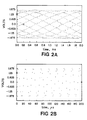
- FIG. 1 (a) a waveform is shown as accurately reconstructed by the digital oscilloscope.
- the Nyquist alias of the same waveform is shown in FIG. 1 (b). Both waveforms appear acceptable to a user expecting to see a sine wave. The frequency of the waveform under test in both FIG. 1.(a) and FIG.
- the frequency of the waveform displayed in FIG. 1(a) appears to be approximately 1.0 MHz.
- the error in the waveform reconstruction of FIG. 1(b) occurred because the sampling rate was not fast enough to allow sufficient data to be acquired to accurately replicate the waveform under test.
- the sampling rate for FIG. 1(a) is 200 MHz, or approximately 200 points or samples per cycle. This is approximately 100 times the number of points needed to accurately reproduce the waveform.
- the sampling rate for FIG. 1(b) is 500 kHz, or approximately one point or sample for every two cycles. This is approximately one- quarter of the number of points needed to accurately reproduce the waveform. Since the sampling rate for the oscilloscope which produced the waveforms in FIG.16 and FIG. 1(b) is always 1024 points per time frame, the frequency of the tested signal must be less than 512 cycles per time frame to avoid Nyquist aliasing.
- the alias test is performed on a time frame prior to the actual trigger point.
- a delay counter is used to vary the testing time frame with reference to the time frame displayed to the user. Another embodiment automatically increases the sample rate until Nyquist aliasing no longer occurs.
- Perceptual aliasing occurs when the waveform is accurately replicated on the display by the oscilloscope, but the sampled points occur in such a fashion as to lead the user to make a visual misinterpretation. For example, if exactly four points per cycle of a sinusoidal wave were captured, at the maximum value, the minimum value, and the value where the waveform is equal to the dc offset, and the display scaling was set to cover a large amount of time relative to the period of the wave, the user would tend to see three horizontal lines on the display, one equal to the maximum value, one equal to the minimum value, and one equal to the dc offset, instead of seeing a sinusoidal wave with a frequency which is very fast compared to the time period displayed.
- FIG. 2(a) More typically, a perceptual aliasing problem will appear as several distinct signals placed on the same display, as shown in FIG. 2(a).
- This replication may appear confusing to a user expecting a sine wave.
- the waveform is FIG. 2(a) has a frequency of approximately 41.9 kHz.
- the duration of the time frame is 2 ms. This means that between 80 and 90 cycles of the waveform are displayed in FIG. 2(a).
- FIG. 2(b) the section of FIG. 2(a) between the X cursor and the O cursor has been expanded to present a less confusing view of the waveform.
- the duration of the time frame in this figure is 200 microseconds. Between 8 and 9 cycles of the waveform are displayed, allowing the waveform to be recognized more easily as a sine wave.
- the user programs the oscilloscope to detect perceptual aliasing according to the user's criteria. If the user criterium was a minimum of 16 sampling points per cycle, and the number of sampling points for the time period was 1024, the maximum number of cycles for that time period would be 61. If the user criteria was a minimum of 20 sampling points per cycle, and the number of sampling points for that time period was 1024, then the maximum number of cycles for that time period would be 51. If perceptual aliasing as defined by the users criteria is detected, the user could compensate for the problem by increasing the sampling rate or by decreasing the period of the display graph. Another embodiment would make these adjustments automatically.
- Block 10 shows the analog-to-digital converters for channel 1 and channel 2, elements 12 and 14.
- a microprocessor (CPU), element 18, is responsible for coordinating the acquisition process.
- the master set line not shown, is activated by the microprocessor (CPU) prior to the acquisition process to set the initial conditions for the flags and counters.
- the microprocessor starts the sample clock element 16.
- the clock enables the analog-to-digital converters to take samplings at the user-determined sampling rate.
- the sample clock output which is a series of clocking pulses as shown in FIG. 4, also goes to block 30.
- Block 10 shows some components being used in the oscilloscope during alias testing and sampling.
- the incoming signal or waveform to be tested is converted to a square wave signal with a fundamental frequency equal to the fundamental frequency of the incoming signal.
- the incoming signal enters block 20 on line 21 and enters a comparator, element 22.
- the signal is the trigger level set by the user.
- the output of the comparator is twovalued, high when the input on line 21 is greater than the input on line 23, and low when the input on line 23 is greater than the input on line 2. If the user chooses a trigger level properly, the value of the comparator will toggle between high and low at the same frequency as the fundamental frequency of the waveform to be tested. This produces a square wave version of the incoming signal called the AUTOCLOCK (A.C.).
- FIG.4 An example of a TRIGGER SIGNAL and a TRIGGER LEVEL is shown in FIG.4, along with the corresponding AUTOCLOCK.
- the AUTOCLOCK feeds into a divide by-two unit, element 24, and is divided by two, as shown in FIG.4 as the A.C./2.
- the start flag for the frequency counter is enabled which begins the acquisition interval, the number of samples to be taken after the start of the acquisition interval is counted, and then the stop flag is enabled ending the acquisition interval.
- the sample clock output from the sample clock, element 16 in block 10 is the input for a divide-by-four unit, element 32 in block 30.
- the divide-by-four unit is two divide-by-two units in series.
- the timing diagram of FIG.4 shows the output of the various stages as the SAMPLE CLOCK (S.C.), the S.C./2, and the S.C./4.
- the output of the divide-by-four, S.C./4 has one leading edge and one falling edge for every 4 leading edges and 4 falling edges of the SAMPLE CLOCK.
- the output S.C./4 goes to the Low Start Flag, element 36, which goes low on the first leading edge of the Low S.C./4 clock.
- the Start Flag was set high when the CPU, element 18, pulsed the master set prior to the beginning of the acquisition interval.
- the Start Flag can be a D-type flip-flop in a latch configuration.
- a D-type flip-flop is a logical unit with 5 inputs and 2 outputs.
- the primary output is Q
- the other output is Q, the inverse of Q.
- the first two inputs are the D input and the clock input.
- Q On the leading edge of the clock pulse, Q becomes whatever D was just prior to the clock's leading edge.
- the Q output remains constant until the next leading edge of the clock, when it becomes whatever D was prior to the clock leading edge again.
- the third input is the enable. When the flip-flop is enabled, it responds to the D input and clock input. When it is not enabled, the D-type flip-flop has a constant output on Q of whatever Q was
- the last two inputs, the set and the reset are for setting the initial conditions of the flip-flop.
- a positive pulse on the set makes the Q output high; a positive pulse on the reset makes the Q output a zero, bypassing the D input and clock input, and placing an initial condition on Q prior to the first leading edge of the clock.
- the Low Start Flag is always enabled.
- the D input is pinned low.
- the clock input is S.C./4, the output of the divide-by-four unit, element 32.
- the divide-by-four unit output is also used to clock an 8-bit memory address counter, element 34, which has been preset to zero by the CPU, element 18.
- a terminal count indicator is enabled low for one S.C./4 pulse as shown in the timing diagram of FIG. 4 at MAC T.C (memory address counter terminal count).
- the acquisition interval may vary in length of time but the number of samples taken during the interval, 1024, is always the same for this embodiment. Since the memory address counter counts once for every four sample clock pulses, it will have counted 1024 samples when it reaches 256 and enables the terminal count low. The memory address counter is used to stop the frequency counter at the end of the acquisition interval.
- the High Stop Flag, element 38 can be a D-type flip-flop similar to the Low Start Flag, also set up in a latch configuration.
- the enable is the terminal count of the memory address counter, MAC T.C., and will only allow the latch to function when the MAC T.C. goes low as shown at High Stop Flag in FIG. 4.
- the D input is pinned low
- the clock input is the S.C./4
- the output is Q
- the inverse of Q and the set is on the master set line from the CPU.
- This means Q or the High Stop Flag will be set low prior to the beginning of the acquisition interval by the master set, and will be enabled by the memory address counter terminal count, MAC T. C., and will go high on the next leading edge of the clock input during enablement, which will be the 256th positive edge of S.C./4.
- the stop flag will remain high until the Q output is set by the master set of the CPU, element 18.
- the output from the Stop Flag goes to the trigger, element 44 in block 40.
- the High Stop Flag output goes high on the 256th leading edge of S.C./4, it also enables the trigger to look for the triggering event defined by the user as shown at High Analog Trigger Arm in FIG. 4.
- the trigger output goes and signals the delay counter, element 42, to count the delay specified by the user, and then stop the acquisition there as shown at Low Analog Trigger in FIG.4.
- the display will show points sampled during the acquisition interval, which is immediately prior to the end of the delay counted by the delay counter element 42.
- both LOW START FLAG and HIGH STOP FLAG enter the Low Count Enable Gate which is element 52, a two-input OR.
- the OR output is high whenever one input or the other input or both inputs are high. Only when both inputs are low is the output low. Since the initial state of the Low Start Flag is high, and the initial state of the High Stop Flag is low, the OR output is high.
- the OR output, or Low Count Enable Gate goes low and stays low until the HIGH STOP FLAG goes high.
- the output of the Low Count Enable Gate is shown in FIG.4, the timing diagram.
- the frequency counter, element 54 can be an 8- bit counter similar to the memory address counter, element 34. Prior to the start of the acquisition period, the frequency counter will have been reset to zero by the CPU, element 18. The frequency counter is enabled only while the LOW COUNT ENABLE GATE is low. The frequency counter will count the pulses on the clock line during the time that it is enabled.
- the clock line is A.C./2 and has one pulse for every two cycles of the waveform under test, TRIGGER SIGNAL.
- the terminal count line will be enabled low, as shown at FREQUENCY COUNTER T.C., in FIG. 4, the timing diagram. If there are more than 512 cycles of the waveform under test, which is 256 A.C./2 pulses, the terminal count will go low for one clock pulse.
- the High Alias Flag may be a latch built with a D-type flip-flop, similar to the Low Start Flag and the High Stop Flag.
- the FREQUENCY COUNTER T.C. would be the enable of the flip-flop.
- the set would be connected to the master set line.
- the D input would always be low.
- the clock would be the A.C./2.
- the Q line would start high, and then go low and stay there till the master set is pulsed again.
- the Q line or HIGH ALIAS FLAG would be the output to block 60.
- the HIGH ALIAS FLAG would start low, and then go high, complementing the Q output and is shown in FIG.4.
- the HIGH ALIAS FLAG is sent to the CPU I/O port, element 62, where the CPU, element 18, is looking for the HIGH ALIAS FLAG.
- the CPU interprets the high state of the HIGH ALIAS FLAG as meaning that the sample rate is too slow and an Nyquist aliased condition exists.
- the CPU displays an alias warning to the user.
- the user may not have been aware of the false replication of the waveform and the alias warning prompts the user to increase the sampling rate and force accurate replication of TRIGGER SIGNAL, the waveform.
- the CPU, element 18 increases the sampling rate automatically until the signal is not aliased, instead of displaying a warning to the user. This could be readily implemented through the CPU software. As the HIGH ALIAS FLAG is enabled, the CPU increases the sampling rate and tests the HIGH ALIAS FLAG. If it is enabled at the end of another acquisition interval, the sampling rate is increased again. This process continues until the HIGH ALIAS FLAG indicates that aliasing is not occurring. The sampling rate could be displayed to the user so that the user is aware of the change in sampling rate. Another embodiment would compute the correct sampling rate and implement it automatically.
- An alternate embodiment could allow the user to test for perceptual aliasing according to the user's own criteria.
- a test for perceptual aliasing could be made by comparing the sampling rate against the frequency of the incoming signal, according to user-specified criterion, for example, 16 points per cycle or 20 points per cycle. If the criterion was met, the display would be more likely to replicate the waveform without causing a perceptual aliasing problem to the user. If the comparison fails the user criterion, a warning could be displayed to the user, or the sampling rate could be automatically increased to allow the user-programmed perceptual aliasing criterion to be met.
- the alias testing may occur during a time frame prior to the time frame displayed to the user.
- the alias testing may be done for the time frame actually displayed to the user, or for a time frame occurring after the time frame displayed to the user.
- the delay counter could be used to begin or end the acquisition period in reference to the beginning or end of the alias test period. The length of the delay could be set by the user.
Landscapes
- Physics & Mathematics (AREA)
- General Physics & Mathematics (AREA)
- Nonlinear Science (AREA)
- Tests Of Electronic Circuits (AREA)
- Analogue/Digital Conversion (AREA)
- Measurement Of Radiation (AREA)
Claims (8)
Applications Claiming Priority (2)
| Application Number | Priority Date | Filing Date | Title |
|---|---|---|---|
| US06/668,776 US4656598A (en) | 1984-11-06 | 1984-11-06 | Alias detector for digital oscilloscopes |
| US668776 | 1984-11-06 |
Publications (2)
| Publication Number | Publication Date |
|---|---|
| EP0181565A1 EP0181565A1 (fr) | 1986-05-21 |
| EP0181565B1 true EP0181565B1 (fr) | 1989-03-22 |
Family
ID=24683687
Family Applications (1)
| Application Number | Title | Priority Date | Filing Date |
|---|---|---|---|
| EP85113814A Expired EP0181565B1 (fr) | 1984-11-06 | 1985-10-30 | Oscilloscope numérique |
Country Status (4)
| Country | Link |
|---|---|
| US (1) | US4656598A (fr) |
| EP (1) | EP0181565B1 (fr) |
| JP (1) | JPS61112291A (fr) |
| DE (1) | DE3569039D1 (fr) |
Families Citing this family (8)
| Publication number | Priority date | Publication date | Assignee | Title |
|---|---|---|---|---|
| US4802098A (en) * | 1987-04-03 | 1989-01-31 | Tektronix, Inc. | Digital bandpass oscilloscope |
| US4888588A (en) * | 1988-10-17 | 1989-12-19 | Tektronix, Inc. | Digital trigger |
| US5010507A (en) * | 1989-01-25 | 1991-04-23 | Westinghouse Electrical Corp. | Sampled digital filter system |
| GB2229536B (en) * | 1989-03-22 | 1993-04-07 | Ferranti Int Signal | Signal processing apparatus and method |
| EP0444875B1 (fr) * | 1990-03-02 | 1997-05-14 | Hewlett-Packard Company | Procédé et dispositif pour augmenter la preformance des systèmes numériques à répétition au hasard |
| JP2732419B2 (ja) * | 1991-11-19 | 1998-03-30 | 松下電器産業株式会社 | エイリアシング検出方法とその装置 |
| US6947043B1 (en) | 2000-03-27 | 2005-09-20 | Tektronix, Inc. | Method of operating an oscilloscope |
| US10845400B2 (en) | 2018-07-20 | 2020-11-24 | Rohde & Schwarz Gmbh & Co. Kg | Measurement apparatus and measurement method |
Family Cites Families (8)
| Publication number | Priority date | Publication date | Assignee | Title |
|---|---|---|---|---|
| US3156899A (en) * | 1962-05-24 | 1964-11-10 | Space Technology Lab Inc | Sampled data simulator control system |
| FR2381313A2 (fr) * | 1975-12-31 | 1978-09-15 | Labo Electronique Physique | Enregistrement et visualisation de signaux |
| JPS6053938B2 (ja) * | 1978-06-02 | 1985-11-28 | 大日本スクリ−ン製造株式会社 | アナログ信号のサンプリング方法 |
| US4283713A (en) * | 1979-01-15 | 1981-08-11 | Tektronix, Inc. | Waveform acquisition circuit |
| US4313195A (en) * | 1979-04-23 | 1982-01-26 | Sangamo Weston, Inc. | Reduced sample rate data acquisition system |
| US4271486A (en) * | 1979-07-30 | 1981-06-02 | Tektronix, Inc. | Waveform storage system |
| US4568912A (en) * | 1982-03-18 | 1986-02-04 | Victor Company Of Japan, Limited | Method and system for translating digital signal sampled at variable frequency |
| JPS5948658A (ja) * | 1982-09-13 | 1984-03-19 | Hitachi Denshi Ltd | エイリアシングエラ−検出回路 |
-
1984
- 1984-11-06 US US06/668,776 patent/US4656598A/en not_active Expired - Lifetime
-
1985
- 1985-10-30 EP EP85113814A patent/EP0181565B1/fr not_active Expired
- 1985-10-30 DE DE8585113814T patent/DE3569039D1/de not_active Expired
- 1985-11-06 JP JP60248665A patent/JPS61112291A/ja active Pending
Also Published As
| Publication number | Publication date |
|---|---|
| US4656598A (en) | 1987-04-07 |
| JPS61112291A (ja) | 1986-05-30 |
| DE3569039D1 (en) | 1989-04-27 |
| EP0181565A1 (fr) | 1986-05-21 |
Similar Documents
| Publication | Publication Date | Title |
|---|---|---|
| JP2733746B2 (ja) | ロジック信号表示方法 | |
| EP0234883B1 (fr) | Appareil et procédé pour un échantillon répétitif au hasard | |
| JP2640224B2 (ja) | デジタルオシロスコープに表示スケーリングおよびトリガを与えるために入力信号を分析する方法 | |
| US4438404A (en) | Signal sampling system | |
| US6137283A (en) | Process and machine for signal waveform analysis | |
| GB2100011A (en) | Multi-speed logic analyzer | |
| WO1996026448A9 (fr) | Procede et machine pour l'analyse de la forme d'onde de signaux | |
| EP0515028B1 (fr) | Détection automatique d'événements anormales | |
| JP3561285B2 (ja) | 信号の擬似ランダム反復サンプリング | |
| EP0506223A2 (fr) | Topologie de mise à l'échelle automatique et très rapide pour oscilloscope numérique | |
| EP0740161A2 (fr) | Oscilloscope digital avec déclenchement basé sur reconnaissance d'un schéma | |
| EP0181565B1 (fr) | Oscilloscope numérique | |
| US9874587B1 (en) | One-pass trigger jitter reduction for digital instruments | |
| KR100576226B1 (ko) | 인터리브형 디지털 피크 검출기 | |
| EP0294162B1 (fr) | Sonde vidéo numérique | |
| JPH02231576A (ja) | スペクトラムアナライザ | |
| US4884020A (en) | Phase detection system | |
| US6856924B2 (en) | Mixer-based timebase for sampling multiple input signal references asynchronous to each other | |
| US3946306A (en) | Ignition coil and capacitor analyzer utilizing the zero cross overs and peak voltage of the low coil ringing voltage | |
| US3946305A (en) | Ignition coil and capacitor analyzer utilizing the zero cross-overs and peak voltage of the low coil ringing voltage | |
| US5585819A (en) | Method and apparatus for detecting aliasing | |
| JPH05273245A (ja) | メタステーブル状態検出装置 | |
| SU1659894A1 (ru) | Устройство дл сличени частот | |
| SU1173339A1 (ru) | Цифровой интегрирующий фазометр | |
| SU1275312A1 (ru) | Цифровое устройство дл сравнени частот |
Legal Events
| Date | Code | Title | Description |
|---|---|---|---|
| PUAI | Public reference made under article 153(3) epc to a published international application that has entered the european phase |
Free format text: ORIGINAL CODE: 0009012 |
|
| AK | Designated contracting states |
Kind code of ref document: A1 Designated state(s): DE FR GB NL |
|
| 17P | Request for examination filed |
Effective date: 19860812 |
|
| 17Q | First examination report despatched |
Effective date: 19880825 |
|
| GRAA | (expected) grant |
Free format text: ORIGINAL CODE: 0009210 |
|
| AK | Designated contracting states |
Kind code of ref document: B1 Designated state(s): DE FR GB NL |
|
| REF | Corresponds to: |
Ref document number: 3569039 Country of ref document: DE Date of ref document: 19890427 |
|
| ET | Fr: translation filed | ||
| PLBE | No opposition filed within time limit |
Free format text: ORIGINAL CODE: 0009261 |
|
| STAA | Information on the status of an ep patent application or granted ep patent |
Free format text: STATUS: NO OPPOSITION FILED WITHIN TIME LIMIT |
|
| 26N | No opposition filed | ||
| PGFP | Annual fee paid to national office [announced via postgrant information from national office to epo] |
Ref country code: DE Payment date: 19970925 Year of fee payment: 13 |
|
| PG25 | Lapsed in a contracting state [announced via postgrant information from national office to epo] |
Ref country code: DE Free format text: LAPSE BECAUSE OF NON-PAYMENT OF DUE FEES Effective date: 19990803 |
|
| NLS | Nl: assignments of ep-patents |
Owner name: AGILENT TECHNOLOGIES, INC A DELAWARE CORPORATION;H |
|
| REG | Reference to a national code |
Ref country code: GB Ref legal event code: 732E |
|
| REG | Reference to a national code |
Ref country code: FR Ref legal event code: TP |
|
| REG | Reference to a national code |
Ref country code: FR Ref legal event code: TP |
|
| REG | Reference to a national code |
Ref country code: GB Ref legal event code: IF02 |
|
| PGFP | Annual fee paid to national office [announced via postgrant information from national office to epo] |
Ref country code: FR Payment date: 20021002 Year of fee payment: 18 |
|
| PGFP | Annual fee paid to national office [announced via postgrant information from national office to epo] |
Ref country code: NL Payment date: 20021011 Year of fee payment: 18 |
|
| PGFP | Annual fee paid to national office [announced via postgrant information from national office to epo] |
Ref country code: GB Payment date: 20031022 Year of fee payment: 19 |
|
| PG25 | Lapsed in a contracting state [announced via postgrant information from national office to epo] |
Ref country code: NL Free format text: LAPSE BECAUSE OF NON-PAYMENT OF DUE FEES Effective date: 20040501 |
|
| PG25 | Lapsed in a contracting state [announced via postgrant information from national office to epo] |
Ref country code: FR Free format text: LAPSE BECAUSE OF NON-PAYMENT OF DUE FEES Effective date: 20040630 |
|
| NLV4 | Nl: lapsed or anulled due to non-payment of the annual fee |
Effective date: 20040501 |
|
| REG | Reference to a national code |
Ref country code: FR Ref legal event code: ST |
|
| PG25 | Lapsed in a contracting state [announced via postgrant information from national office to epo] |
Ref country code: GB Free format text: LAPSE BECAUSE OF NON-PAYMENT OF DUE FEES Effective date: 20041030 |
|
| GBPC | Gb: european patent ceased through non-payment of renewal fee |
Effective date: 20041030 |