EP0181059A2 - Semiconductor integrated circuit for clock distribution - Google Patents
Semiconductor integrated circuit for clock distribution Download PDFInfo
- Publication number
- EP0181059A2 EP0181059A2 EP85305969A EP85305969A EP0181059A2 EP 0181059 A2 EP0181059 A2 EP 0181059A2 EP 85305969 A EP85305969 A EP 85305969A EP 85305969 A EP85305969 A EP 85305969A EP 0181059 A2 EP0181059 A2 EP 0181059A2
- Authority
- EP
- European Patent Office
- Prior art keywords
- clock
- clock signal
- signal lines
- drivers
- integrated circuit
- Prior art date
- Legal status (The legal status is an assumption and is not a legal conclusion. Google has not performed a legal analysis and makes no representation as to the accuracy of the status listed.)
- Granted
Links
Images

Classifications
-
- H—ELECTRICITY
- H03—ELECTRONIC CIRCUITRY
- H03K—PULSE TECHNIQUE
- H03K5/00—Manipulating of pulses not covered by one of the other main groups of this subclass
-
- G—PHYSICS
- G06—COMPUTING; CALCULATING OR COUNTING
- G06F—ELECTRIC DIGITAL DATA PROCESSING
- G06F1/00—Details not covered by groups G06F3/00 - G06F13/00 and G06F21/00
- G06F1/04—Generating or distributing clock signals or signals derived directly therefrom
- G06F1/10—Distribution of clock signals, e.g. skew
Definitions
- This invention relates to a semiconductor integrated circuit device, and, more particularly, to the improvement of the clock driver section of a large scale integrated circuit (abbreviated as LSI).
- LSI large scale integrated circuit
- a large number of gate circuits and flip-flop circuits are operated in synchronization with a clock signal. Consequently, a clock signal line which extends all over an LSI chip is connected to numerous load circuits.
- the total capacity of all the load circuits amounts to as much as scores of hundreds of [pF] units.
- a clock driver for actuating a clock signal line connected to such a large capacity load must have a large drivability.
- one output signal from the clock generator 21 is supplied to two divided clock drivers 22 1 , 22 20
- These clock drivers 22 1 , 22 2 supply clock signals CL 1 , CL 2' respectively, to their corresponding clock signal lines 23 1 , 23 1 .
- the clock drivers 22 1 , 22 2 indicate different delay properties, depending on the load condition.
- Fig. 10 indicates the waveforms of the clock signals CL 1 , CL 2 .
- the characters tp l , tp 2 represent the length of time required for the clock signals CL 1 , CL 2 , respectively, to have their logic data converted from "1" to "0".
- a difference Atp between the two lengths of time denote a clock skew. This clock skew adversely affects the operation of the subject semiconductor integrated circuit device.
- Fig. 11 showing the operation of a shift register comprising a plurality of successively connected J-K flip-flop circuits.
- the flip-flop circuit 24 1 of the nth order is operated by the clock signal CL l of Fig. 10.
- the flip-flop circuit 24 2 of the n+lth order, and the flip-flop circuit 24 3 of the n+2th order are operated alike by the clock signal CL 2 of Fig. 10. If the length of time required for the negative edge trigger type flip-flop circuit of Fig.
- the object of this invention to provide a semiconductor integrated circuit device which comprises a plurality of divided clock drivers, and which has resolved the problem of the aforementioned clock skew.
- this invention provides a semiconductor integrated circuit device wherein one output signal from a clock generator is supplied to a plurality of clock signal lines, having one or more load circuits, through a plurality of divided clock drivers.
- the plural clock signal lines are connected together by a common connecting line.
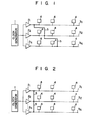
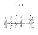
- Fig. 1 is an equivalent circuit of an LSI device according to one embodiment of this invention.
- This LSI device is formed on a semiconductor chip substrate (not shown) by the known manufacturing process.
- Reference numeral 1 denotes a clock generator.
- One output terminal of said clock generator 1 is connected to a plurality of clock drivers (2 1 , 2 2 , ... 2 N ). These clock drivers are properly distributed over the surface of the LSI chip substrate.
- Reference numerals 3 1 , ... 3N represent clock signal lines drawn out independently from the respective clock pulse driver output terminals.
- the clock signal lines 3 are connected to one or more load circuits 4, each of which has to be supplied with a clock signal.
- a common clock signal is supplied to all load circuits 4 through the independent clock signal lines 3 1 - 3 N .
- the clock signal lines 3 1 - 3 N are collectively connected by a common connecting line 5, said common connecting line 5 being metal wire in this embodiment. (For better understanding, said common connecting line 5 is shown in this and subsequent embodiments as a thick line.)
- the independent clock signal lines 3 1 - 3 N are connected together by the common connecting line 5, thus equalizing the load conditions of the plural clock drivers 2. Consequently, clock signals issue from the respective clock drivers 2 without delay, thereby substantially eliminating the occurrence of the clock skew. Since, as described above, the plural clock drivers 2 are properly distributed over the surface of the chip substrate, it is possible to resolve various problems which might arise from large local current variations, were only a single clock driver provided.
- the clock signal lines may be connected by a common connecting line at any point on said clock signal lines. If all the clock signal lines are connected together by the shortest common connecting line, no appreciable increase will result in the wire capacity. If the distributed clock drivers have a sufficient driving power in the aggregate, no consideration has to be given to any increase in the wiring capacity resulting from the provision of the common connecting line. Therefore, automatic placement and routing by computer can easily be applied.
- Figs. 2 and 3 show the LSI devices embodying this invention, wherein the common connecting line for connecting the respective clock signal lines are set at different points from those indicated in Fig. 1.
- the common connecting line 5 is provided right near the output terminals of the clock drivers 2 1 - 2 N .
- the common connecting line 5 is set at a point furthest away from the respective clock drivers 2 1 - 2 N in a relationship entirely opposite to that of Fig. 2.
- the common connecting line 5 for connecting all the clock signal lines together need not be prepared from a metal, but may be formed of, for example, a polycrystalline silicon layer deposited on the chip substrate, or an impurity doped layer formed in the chip substrate.
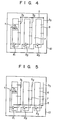
- Fig. 4 is a plan view of a CMOS gate array to which the semiconductor integrated circuit device of this invention is applied.
- a plurality of CMOS cell arrays 6 are mounted on the chip substrate 10. Interstices between the respective cell arrays 6 constitute wiring regions 7.
- a clock generator 1 is constituted by a plurality of CMOS cells involved in each cell array 6.
- Clock drivers 2 1 , 2 2 , 2 3 are constituted by one or more CMOS cells provided at one end of each cell array 6.
- First At wires extend in X direction parallel with the cell array 6.
- Second At wires extend in Y direction perpendicularly intersecting said Y direction.
- the clock signal lines 31, 3 2 , 3 3 extending from the corresponding clock drivers 2 1 , 2 2 , 2 3 are formed of the first At wire layer.
- a common connecting line 5 connecting the clock signal lines 3 1 , 3 2 , 3 3 together is prepared from a second Al layer and lies furthest from the clock drivers 2 1 , 2 2 , 2 3
- Figs. 5 to 7 indicate a CMOS gate array modified from the embodiment of Fig. 4.
- a common connecting line 5 connecting the clock signal lines 3 1 , 3 2t 3 3 together is prepared from a second Al wire layer and lies close to the output terminals of the clock drivers 2 1 , 2 2 , 2 3 .
- the clock driver 2 1 is set in the lowest position of a first cell array; the clock pulse driver 2 2 is positioned at the midpoint of a second cell array; and the clock pulse driver 2 3 lies in the uppermost position of a third cell array.
- a common connecting line connecting the clock signal lines 3 1 , 3 2 , 3 3 together is prepared from a second Al wire layer.
- a common connecting line connecting the clock signal lines 3 1 , 3 2 , 3 3 3 extends in both X and Y directions so as to substantially surround the region in which the cell arrays 6 are formed.
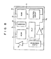
- Fig. 8 is a plan view of an LSI device, according to another embodiment of this invention, which is provided with a memory function.
- ROM read only memory
- RAM random access memory
- decoder decoder
- ALU arithmetic logic unit
- control circuit 15 A clock generator 1 which transmits a clock signal to said circuit elements is set in the corner of the chip substrate 10.
- Reference numerals 2 1 , 2 2 represent divided clock drivers.
- One clock driver 2 1 is intended to supply a clock signal to ROM 11, RAM 13 and decoder 12. This clock driver 2 1 has a relatively small drivability.
- the other clock driver 2 2 is intended to supply a clock signal to ALU 14 and control circuit 15, and has a greater drivability than the clock driver 2 1 .
- These clock drivers 2 1 , 2 2 are set in the vacant regions of the chip substrate 10.
- the clock signal line 3 1 drawn from the output terminal of the clock driver 2 1 , and the clock signal line 3 2 extending from the output terminal of the clock driver 2 2' are connected together by a common connecting line 5 formed in an elongated vacant area extending along part of the periphery of the chip substrate 10. Even the LSI device according to the embodiment of Fig. 8 can effectively eliminate the clock skew, thereby ensuring a reliable logic operation.
Abstract
Description
- This invention relates to a semiconductor integrated circuit device, and, more particularly, to the improvement of the clock driver section of a large scale integrated circuit (abbreviated as LSI).
- With reference to the LSI, a large number of gate circuits and flip-flop circuits are operated in synchronization with a clock signal. Consequently, a clock signal line which extends all over an LSI chip is connected to numerous load circuits. The total capacity of all the load circuits amounts to as much as scores of hundreds of [pF] units. A clock driver for actuating a clock signal line connected to such a large capacity load must have a large drivability.
- When a clock driver having a large drivability is set in the LSI, the following difficulties are encountered.
- (1) A large current change appears in the clock driver section leading to the occurrence of local switching noises, potential changes in a power line, and also a prominent flow of substrate current. As a result, drawbacks arise in that the circuit malfunctions, and the CMOS-LSI becomes subject to breakage resulting from latch-up phenomenon.
- (2) It has been proposed to lay a broad power line and ground line near the clock driver as a means of resolving the above-mentioned problems. However, this process presents difficulties in the drawing of a pattern layout on the LSI. Particularly with automatic placement and routing by a computer, the wiring width is generally restricted, making it difficult to locally broaden a power line.
- (3) A clock pulse is supplied from a single clock driver to a plurality of load circuits distributed over the LSI chip substrate. Consequently, signal lines around the clock driver are extremely congested, another factor presenting difficulties in defining a pattern layout.
- For the resolution of the aforementioned drawbacks, it has hitherto been attempted to distribute a plurality of clock drivers generating the same clock signal over a plurality of points on the LSI chip substrate. This process can, indeed, resolve the problems described in the foregoing items (1) to (3). The mere distribution of the clock drivers, however, is itself accompanied by a drawback related to the clock skew.
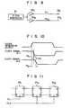
- Description may now be made of this problem with reference to the accompanying Fig. 9. In the example of Fig. 9, one output signal from the
clock generator 21 is supplied to two dividedclock drivers clock drivers clock signal lines clock drivers - Fig. 10 indicates the waveforms of the clock signals CL1, CL2. The characters tpl, tp2 represent the length of time required for the clock signals CL1, CL2, respectively, to have their logic data converted from "1" to "0". A difference Atp between the two lengths of time denote a clock skew. This clock skew adversely affects the operation of the subject semiconductor integrated circuit device.
- In this connection, reference is made to Fig. 11, showing the operation of a shift register comprising a plurality of successively connected J-K flip-flop circuits. The flip-
flop circuit 241 of the nth order is operated by the clock signal CLl of Fig. 10. The flip-flop circuit 242 of the n+lth order, and the flip-flop circuit 243 of the n+2th order are operated alike by the clock signal CL2 of Fig. 10. If the length of time required for the negative edge trigger type flip-flop circuit of Fig. 10 to have its logic data changed from "1" to "0" happens to be shorter than the aforesaid clock skew Atp, then the flip-flop circuit 241 of the nth order has its condition changed before the flip-flop circuit 242 of the n+lth order is triggered. As a result, incorrect data is transmitted to the flip-flop circuit 242 of the n+lth order. If, therefore, a clock driver is simply divided into a plurality of components, the semiconductor integrated circuit device will malfunction, causing, for example, incorrect data to be transmitted due to a different load condition of the clock driver. - It is, accordingly, the object of this invention to provide a semiconductor integrated circuit device which comprises a plurality of divided clock drivers, and which has resolved the problem of the aforementioned clock skew.
- To attain the above-mentioned object, this invention provides a semiconductor integrated circuit device wherein one output signal from a clock generator is supplied to a plurality of clock signal lines, having one or more load circuits, through a plurality of divided clock drivers. The plural clock signal lines are connected together by a common connecting line.
- This invention can be more fully understood from the following detailed description when taken in conjunction with the accompanying drawings, in which:
- Fig. 1 is an equivalent circuit of an LSI device according to one embodiment of this invention;
- Figs. 2 and 3 are the equivalent circuits of the LSI devices according to the other embodiments of the invention;
- Figs. 4 to 7 are typical plan views of a gate array provided with the semiconductor integrated circuit device of the invention;
- Fig. 8 is a plan view of a certain logic LSI device possessed of a memory function to which the semiconductor integrated circuit device of the invention is applied;
- Fig. 9 shows an equivalent circuit indicating the fundamental arrangement of divided clock drivers type LSI device; and
- Figs. 10 and 11 are illustrations given to explain the clock skew problem which may occur in Fig. 9.
- Fig. 1 is an equivalent circuit of an LSI device according to one embodiment of this invention. This LSI device is formed on a semiconductor chip substrate (not shown) by the known manufacturing process.
Reference numeral 1 denotes a clock generator. One output terminal ofsaid clock generator 1 is connected to a plurality of clock drivers (21, 22, ... 2N). These clock drivers are properly distributed over the surface of the LSI chip substrate. Reference numerals 31, ... 3N represent clock signal lines drawn out independently from the respective clock pulse driver output terminals. The clock signal lines 3 are connected to one ormore load circuits 4, each of which has to be supplied with a clock signal. More specifically, a common clock signal is supplied to allload circuits 4 through the independent clock signal lines 31 - 3N. The clock signal lines 31 - 3N are collectively connected by a common connectingline 5, said common connectingline 5 being metal wire in this embodiment. (For better understanding, said common connectingline 5 is shown in this and subsequent embodiments as a thick line.) - As described above, the independent clock signal lines 31 - 3N are connected together by the common connecting
line 5, thus equalizing the load conditions of theplural clock drivers 2. Consequently, clock signals issue from therespective clock drivers 2 without delay, thereby substantially eliminating the occurrence of the clock skew. Since, as described above, theplural clock drivers 2 are properly distributed over the surface of the chip substrate, it is possible to resolve various problems which might arise from large local current variations, were only a single clock driver provided. - It is advised that a circuit designer define the drivability of the
entire clock driver 2 in consideration of the operation speed of theload circuits 4 connected to the clock signal lines 3 and subjected to the most rigid timing conditions, and also of the capacity of all theload circuits 4. Further, it is advised that the clock drivers be properly distributed in accordance with the power line width and the space on the surface of the LSI chip substrate, so that all the distributed drivers may have the drivability prescribed for an entire clock pulse driving unit. The above-mentioned arrangement will quickly resolve the difficulty of designing a circuit involving distributed clock drivers. - The clock signal lines may be connected by a common connecting line at any point on said clock signal lines. If all the clock signal lines are connected together by the shortest common connecting line, no appreciable increase will result in the wire capacity. If the distributed clock drivers have a sufficient driving power in the aggregate, no consideration has to be given to any increase in the wiring capacity resulting from the provision of the common connecting line. Therefore, automatic placement and routing by computer can easily be applied.
- Figs. 2 and 3 show the LSI devices embodying this invention, wherein the common connecting line for connecting the respective clock signal lines are set at different points from those indicated in Fig. 1. In Fig. 2, the common connecting
line 5 is provided right near the output terminals of the clock drivers 21 - 2N. In Fig. 3, the common connectingline 5 is set at a point furthest away from the respective clock drivers 21 - 2N in a relationship entirely opposite to that of Fig. 2. Further, it is possible to connect clock signal lines at several points by the common connectingline 5 in so far as an increase in the load capacity can be overlooked; for example, to combine the embodiments of Figs. 2 and 3. - The common connecting
line 5 for connecting all the clock signal lines together need not be prepared from a metal, but may be formed of, for example, a polycrystalline silicon layer deposited on the chip substrate, or an impurity doped layer formed in the chip substrate. - Fig. 4 is a plan view of a CMOS gate array to which the semiconductor integrated circuit device of this invention is applied. A plurality of
CMOS cell arrays 6 are mounted on thechip substrate 10. Interstices between therespective cell arrays 6 constitutewiring regions 7. Aclock generator 1 is constituted by a plurality of CMOS cells involved in eachcell array 6.Clock drivers cell array 6. First At wires extend in X direction parallel with thecell array 6. Second At wires extend in Y direction perpendicularly intersecting said Y direction. Theclock signal lines 31, 32, 33 extending from thecorresponding clock drivers line 5 connecting the clock signal lines 31, 32, 33 together is prepared from a second Aℓ layer and lies furthest from theclock drivers - Figs. 5 to 7 indicate a CMOS gate array modified from the embodiment of Fig. 4. Referring to Fig. 5, a common connecting
line 5 connecting the clock signal lines 31, 32t 33 together is prepared from a second Aℓ wire layer and lies close to the output terminals of theclock drivers clock driver 21 is set in the lowest position of a first cell array; theclock pulse driver 22 is positioned at the midpoint of a second cell array; and theclock pulse driver 23 lies in the uppermost position of a third cell array. In the case of Fig. 6, too, a common connecting line connecting the clock signal lines 31, 32, 33 together is prepared from a second Aℓ wire layer. In Fig. 7, a common connecting line connecting the clock signal lines 31, 32, 33 extends in both X and Y directions so as to substantially surround the region in which thecell arrays 6 are formed. - Fig. 8 is a plan view of an LSI device, according to another embodiment of this invention, which is provided with a memory function. Integrally formed on a
chip substrate 10 are ROM (read only memory) 11, RAM (random access memory) 13,decoder 12, ALU (arithmetic logic unit) 14 andcontrol circuit 15. Aclock generator 1 which transmits a clock signal to said circuit elements is set in the corner of thechip substrate 10.Reference numerals clock driver 21 is intended to supply a clock signal to ROM 11,RAM 13 anddecoder 12. Thisclock driver 21 has a relatively small drivability. Theother clock driver 22 is intended to supply a clock signal toALU 14 andcontrol circuit 15, and has a greater drivability than theclock driver 21. Theseclock drivers chip substrate 10. The clock signal line 31 drawn from the output terminal of theclock driver 21, and the clock signal line 32 extending from the output terminal of theclock driver 22' are connected together by a common connectingline 5 formed in an elongated vacant area extending along part of the periphery of thechip substrate 10. Even the LSI device according to the embodiment of Fig. 8 can effectively eliminate the clock skew, thereby ensuring a reliable logic operation.
Claims (2)
Applications Claiming Priority (2)
| Application Number | Priority Date | Filing Date | Title |
|---|---|---|---|
| JP59204451A JPS6182525A (en) | 1984-09-29 | 1984-09-29 | Semiconductor integrated circuit device |
| JP204451/84 | 1984-09-29 |
Publications (3)
| Publication Number | Publication Date |
|---|---|
| EP0181059A2 true EP0181059A2 (en) | 1986-05-14 |
| EP0181059A3 EP0181059A3 (en) | 1987-11-25 |
| EP0181059B1 EP0181059B1 (en) | 1991-02-13 |
Family
ID=16490742
Family Applications (1)
| Application Number | Title | Priority Date | Filing Date |
|---|---|---|---|
| EP85305969A Expired - Lifetime EP0181059B1 (en) | 1984-09-29 | 1985-08-22 | Semiconductor integrated circuit for clock distribution |
Country Status (5)
| Country | Link |
|---|---|
| US (1) | US4661721A (en) |
| EP (1) | EP0181059B1 (en) |
| JP (1) | JPS6182525A (en) |
| KR (1) | KR900000105B1 (en) |
| DE (1) | DE3581754D1 (en) |
Cited By (8)
| Publication number | Priority date | Publication date | Assignee | Title |
|---|---|---|---|---|
| EP0258975A2 (en) * | 1986-07-09 | 1988-03-09 | Eta Systems, Inc. | Clock bus system for an integrated circuit |
| EP0335697A2 (en) * | 1988-03-29 | 1989-10-04 | Kabushiki Kaisha Toshiba | Integrated circuit device comprising interconnection wiring |
| EP0355769A2 (en) * | 1988-08-19 | 1990-02-28 | Kabushiki Kaisha Toshiba | Clock supply circuit |
| EP0362691A2 (en) * | 1988-10-05 | 1990-04-11 | Siemens Aktiengesellschaft | Anti-clock skew distribution apparatus |
| EP0418912A2 (en) * | 1989-09-22 | 1991-03-27 | Kabushiki Kaisha Toshiba | Semiconductor integrated circuit device |
| US5304826A (en) * | 1989-09-22 | 1994-04-19 | Kabushiki Kaisha Toshiba | Semiconductor integrated circuit device |
| DE4422456B4 (en) * | 1993-06-30 | 2004-07-01 | Intel Corporation, Santa Clara | Clock distribution system for a microprocessor |
| DE4447848B4 (en) * | 1993-06-30 | 2005-10-27 | Intel Corporation, Santa Clara | Clock signal distribution and interrupt system for microprocessor integrated circuit device - has number of global drivers uniformly disposed along periphery of integrated circuit and number of feeders for supply clock signals to circuit components of integrated circuit |
Families Citing this family (19)
| Publication number | Priority date | Publication date | Assignee | Title |
|---|---|---|---|---|
| ATE62774T1 (en) * | 1985-09-25 | 1991-05-15 | Siemens Ag | NETWORK FOR PROCESSING DATA WITH A LARGE BIT WIDTH WITH ONE TRANSMITTER AND A NUMBER OF RECEIVERS. |
| JPS63238714A (en) * | 1986-11-26 | 1988-10-04 | Hitachi Ltd | Clock supplying system |
| US5133064A (en) | 1987-04-27 | 1992-07-21 | Hitachi, Ltd. | Data processing system generating clock signal from an input clock, phase locked to the input clock and used for clocking logic devices |
| US5012427A (en) * | 1988-01-30 | 1991-04-30 | Kabushiki Kaisha Toshiba | Semiconductor integrated circuit and method of manufacturing the same |
| JPH02205908A (en) * | 1989-02-03 | 1990-08-15 | Nec Corp | Data processor |
| JPH0824143B2 (en) * | 1989-02-08 | 1996-03-06 | 株式会社東芝 | Placement and wiring method of integrated circuit |
| JPH07101788B2 (en) * | 1989-06-16 | 1995-11-01 | 富士通株式会社 | Duplex device with radio wave emission suppression function |
| US5032743A (en) * | 1990-05-09 | 1991-07-16 | National Semiconductor Corporation | Skew clamp |
| US5396129A (en) * | 1992-05-25 | 1995-03-07 | Matsushita Electronics Corporation | Semiconductor integrated circuit apparatus comprising clock signal line formed in a ring shape |
| US5444407A (en) * | 1992-12-28 | 1995-08-22 | Advanced Micro Devices, Inc. | Microprocessor with distributed clock generators |
| US5438297A (en) * | 1992-12-30 | 1995-08-01 | Intel Corporation | Electrical trace having a closed loop configuration |
| JP3112784B2 (en) * | 1993-09-24 | 2000-11-27 | 日本電気株式会社 | Clock signal distribution circuit |
| US5570054A (en) * | 1994-09-26 | 1996-10-29 | Hitachi Micro Systems, Inc. | Method and apparatus for adaptive clock deskewing |
| US5570053A (en) * | 1994-09-26 | 1996-10-29 | Hitachi Micro Systems, Inc. | Method and apparatus for averaging clock skewing in clock distribution network |
| JPH10242396A (en) * | 1997-03-03 | 1998-09-11 | Mitsubishi Electric Corp | Clock driver circuit and semiconductor integrated circuit device |
| KR100303533B1 (en) * | 1998-03-30 | 2001-11-22 | 윤종용 | Microwave oven |
| US6052012A (en) * | 1998-06-29 | 2000-04-18 | Cisco Technology, Inc. | Method and apparatus for clock uncertainly minimization |
| US6513149B1 (en) | 2000-03-31 | 2003-01-28 | International Business Machines Corporation | Routing balanced clock signals |
| DE102010048160A1 (en) * | 2010-10-11 | 2012-04-12 | Aaa Water Technologies Ag | Multi-stage membrane distillation device |
Citations (2)
| Publication number | Priority date | Publication date | Assignee | Title |
|---|---|---|---|---|
| JPS58166422A (en) * | 1982-03-29 | 1983-10-01 | Fujitsu Ltd | Clock generation system |
| JPS5924324A (en) * | 1982-07-30 | 1984-02-08 | Nec Corp | Integrated circuit device |
Family Cites Families (5)
| Publication number | Priority date | Publication date | Assignee | Title |
|---|---|---|---|---|
| US3104330A (en) * | 1960-02-11 | 1963-09-17 | Gen Electric | Clock pulse distribution system for synchronously driving a plurality of flip-flops |
| US3479603A (en) * | 1966-07-28 | 1969-11-18 | Bell Telephone Labor Inc | A plurality of sources connected in parallel to produce a timing pulse output while any source is operative |
| US3751591A (en) * | 1972-06-20 | 1973-08-07 | Ibm | Zero skew clock distribution system |
| JPS55136726A (en) * | 1979-04-11 | 1980-10-24 | Nec Corp | High voltage mos inverter and its drive method |
| US4504745A (en) * | 1982-06-14 | 1985-03-12 | Rockwell International Corporation | Clocked tri-state driver circuit |
-
1984
- 1984-09-29 JP JP59204451A patent/JPS6182525A/en active Pending
-
1985
- 1985-06-12 KR KR1019850004137A patent/KR900000105B1/en not_active IP Right Cessation
- 1985-08-21 US US06/767,847 patent/US4661721A/en not_active Expired - Lifetime
- 1985-08-22 EP EP85305969A patent/EP0181059B1/en not_active Expired - Lifetime
- 1985-08-22 DE DE8585305969T patent/DE3581754D1/en not_active Expired - Lifetime
Patent Citations (2)
| Publication number | Priority date | Publication date | Assignee | Title |
|---|---|---|---|---|
| JPS58166422A (en) * | 1982-03-29 | 1983-10-01 | Fujitsu Ltd | Clock generation system |
| JPS5924324A (en) * | 1982-07-30 | 1984-02-08 | Nec Corp | Integrated circuit device |
Non-Patent Citations (2)
| Title |
|---|
| PATENT ABSTRACTS OF JAPAN, vol. 8, no. 1 (P-246)[1438], 6th January 1984; & JP-A-58 166 422 (FUJITSU K.K.) 01-10-1983 * |
| PATENT ABSTRACTS OF JAPAN, vol. 8, no. 117 (P-277)[1554], 31st May 1984; & JP-A-59 24 324 (NIPPON DENKI K.K.) 08-02-1984 * |
Cited By (14)
| Publication number | Priority date | Publication date | Assignee | Title |
|---|---|---|---|---|
| EP0258975A3 (en) * | 1986-07-09 | 1989-07-12 | Eta Systems, Inc. | Clock bus system for an integrated circuit |
| EP0258975A2 (en) * | 1986-07-09 | 1988-03-09 | Eta Systems, Inc. | Clock bus system for an integrated circuit |
| EP0335697A3 (en) * | 1988-03-29 | 1990-05-23 | Kabushiki Kaisha Toshiba | Integrated circuit device comprising interconnection wiring |
| EP0335697A2 (en) * | 1988-03-29 | 1989-10-04 | Kabushiki Kaisha Toshiba | Integrated circuit device comprising interconnection wiring |
| EP0355769A3 (en) * | 1988-08-19 | 1990-06-06 | Kabushiki Kaisha Toshiba | Clock supply circuit clock supply circuit |
| EP0355769A2 (en) * | 1988-08-19 | 1990-02-28 | Kabushiki Kaisha Toshiba | Clock supply circuit |
| US5013942A (en) * | 1988-08-19 | 1991-05-07 | Kabushiki Kaisha Toshiba | Clock supply circuit having adjustment capacitance |
| EP0362691A2 (en) * | 1988-10-05 | 1990-04-11 | Siemens Aktiengesellschaft | Anti-clock skew distribution apparatus |
| EP0362691A3 (en) * | 1988-10-05 | 1990-08-16 | Siemens Aktiengesellschaft | Anti-clock skew distribution apparatus |
| EP0418912A2 (en) * | 1989-09-22 | 1991-03-27 | Kabushiki Kaisha Toshiba | Semiconductor integrated circuit device |
| EP0418912A3 (en) * | 1989-09-22 | 1992-01-08 | Kabushiki Kaisha Toshiba | Semiconductor integrated circuit device |
| US5304826A (en) * | 1989-09-22 | 1994-04-19 | Kabushiki Kaisha Toshiba | Semiconductor integrated circuit device |
| DE4422456B4 (en) * | 1993-06-30 | 2004-07-01 | Intel Corporation, Santa Clara | Clock distribution system for a microprocessor |
| DE4447848B4 (en) * | 1993-06-30 | 2005-10-27 | Intel Corporation, Santa Clara | Clock signal distribution and interrupt system for microprocessor integrated circuit device - has number of global drivers uniformly disposed along periphery of integrated circuit and number of feeders for supply clock signals to circuit components of integrated circuit |
Also Published As
| Publication number | Publication date |
|---|---|
| EP0181059A3 (en) | 1987-11-25 |
| KR860002866A (en) | 1986-04-30 |
| EP0181059B1 (en) | 1991-02-13 |
| KR900000105B1 (en) | 1990-01-19 |
| DE3581754D1 (en) | 1991-03-21 |
| JPS6182525A (en) | 1986-04-26 |
| US4661721A (en) | 1987-04-28 |
Similar Documents
| Publication | Publication Date | Title |
|---|---|---|
| EP0181059B1 (en) | Semiconductor integrated circuit for clock distribution | |
| US5045725A (en) | Integrated standard cell including clock lines | |
| EP1129486B1 (en) | Integrated circuit power and ground routing | |
| US4811073A (en) | Gate array arrangement | |
| EP0074825B2 (en) | Manufacture of integrated circuits by masterslice methods | |
| US4893170A (en) | Semiconductor device with multi-level wiring in a gate array | |
| EP0563973B1 (en) | Master slice integrated circuit having a reduced chip size and a reduced power supply noise | |
| EP0612151B1 (en) | Semiconductor device capable of reducing a clock skew in a plurality of wiring pattern blocks | |
| JPS64821B2 (en) | ||
| US5270592A (en) | Clock supply circuit layout in a circuit area | |
| US4851717A (en) | Master slice integrated circuit capable of high speed operation | |
| JPH01246845A (en) | Integrated circuit | |
| EP0021661B1 (en) | Semiconductor master-slice device | |
| EP0416456B1 (en) | Master slice integrated circuit power supply system | |
| JPH0571137B2 (en) | ||
| US4746965A (en) | Integrated semiconductor circuit device | |
| US5401988A (en) | Standard cell layout arrangement for an LSI circuit | |
| JPS61226943A (en) | Standard cell for automatic disposal wiring | |
| KR100329952B1 (en) | Semiconductor integrated circuit and wiring method thereof | |
| US6855967B2 (en) | Utilization of MACRO power routing area for buffer insertion | |
| JPH0518462B2 (en) | ||
| EP0278463B1 (en) | Gate array having transistor buried in interconnection region | |
| JP2642377B2 (en) | Semiconductor integrated circuit device and method of manufacturing the same | |
| KR100390203B1 (en) | Semiconductor integrated circuit | |
| JP2889462B2 (en) | Semiconductor integrated circuit |
Legal Events
| Date | Code | Title | Description |
|---|---|---|---|
| PUAI | Public reference made under article 153(3) epc to a published international application that has entered the european phase |
Free format text: ORIGINAL CODE: 0009012 |
|
| 17P | Request for examination filed |
Effective date: 19850909 |
|
| AK | Designated contracting states |
Kind code of ref document: A2 Designated state(s): DE FR GB |
|
| PUAL | Search report despatched |
Free format text: ORIGINAL CODE: 0009013 |
|
| AK | Designated contracting states |
Kind code of ref document: A3 Designated state(s): DE FR GB |
|
| 17Q | First examination report despatched |
Effective date: 19900404 |
|
| GRAA | (expected) grant |
Free format text: ORIGINAL CODE: 0009210 |
|
| AK | Designated contracting states |
Kind code of ref document: B1 Designated state(s): DE FR GB |
|
| REF | Corresponds to: |
Ref document number: 3581754 Country of ref document: DE Date of ref document: 19910321 |
|
| ET | Fr: translation filed | ||
| PLBI | Opposition filed |
Free format text: ORIGINAL CODE: 0009260 |
|
| 26 | Opposition filed |
Opponent name: TELEFUNKEN ELECTRONIC GMBH Effective date: 19911111 |
|
| PLAB | Opposition data, opponent's data or that of the opponent's representative modified |
Free format text: ORIGINAL CODE: 0009299OPPO |
|
| R26 | Opposition filed (corrected) |
Opponent name: TEMIC TELEFUNKEN MICROELECTRONIC GMBH Effective date: 19911111 |
|
| PGFP | Annual fee paid to national office [announced via postgrant information from national office to epo] |
Ref country code: FR Payment date: 19930805 Year of fee payment: 9 |
|
| PGFP | Annual fee paid to national office [announced via postgrant information from national office to epo] |
Ref country code: GB Payment date: 19930812 Year of fee payment: 9 |
|
| PGFP | Annual fee paid to national office [announced via postgrant information from national office to epo] |
Ref country code: DE Payment date: 19930823 Year of fee payment: 9 |
|
| RDAG | Patent revoked |
Free format text: ORIGINAL CODE: 0009271 |
|
| STAA | Information on the status of an ep patent application or granted ep patent |
Free format text: STATUS: PATENT REVOKED |
|
| 27W | Patent revoked |
Effective date: 19930715 |
|
| GBPR | Gb: patent revoked under art. 102 of the ep convention designating the uk as contracting state |
Free format text: 930715 |