EP0180461A2 - Convertisseurs numériques-analogiques - Google Patents
Convertisseurs numériques-analogiques Download PDFInfo
- Publication number
- EP0180461A2 EP0180461A2 EP85307833A EP85307833A EP0180461A2 EP 0180461 A2 EP0180461 A2 EP 0180461A2 EP 85307833 A EP85307833 A EP 85307833A EP 85307833 A EP85307833 A EP 85307833A EP 0180461 A2 EP0180461 A2 EP 0180461A2
- Authority
- EP
- European Patent Office
- Prior art keywords
- digital
- output
- delay
- summing
- type
- Prior art date
- Legal status (The legal status is an assumption and is not a legal conclusion. Google has not performed a legal analysis and makes no representation as to the accuracy of the status listed.)
- Withdrawn
Links
Images

Classifications
-
- H—ELECTRICITY
- H03—ELECTRONIC CIRCUITRY
- H03M—CODING; DECODING; CODE CONVERSION IN GENERAL
- H03M7/00—Conversion of a code where information is represented by a given sequence or number of digits to a code where the same, similar or subset of information is represented by a different sequence or number of digits
- H03M7/30—Compression; Expansion; Suppression of unnecessary data, e.g. redundancy reduction
- H03M7/3002—Conversion to or from differential modulation
- H03M7/3004—Digital delta-sigma modulation
- H03M7/3015—Structural details of digital delta-sigma modulators
- H03M7/3031—Structural details of digital delta-sigma modulators characterised by the order of the loop filter, e.g. having a first order loop filter in the feedforward path
- H03M7/3033—Structural details of digital delta-sigma modulators characterised by the order of the loop filter, e.g. having a first order loop filter in the feedforward path the modulator having a higher order loop filter in the feedforward path, e.g. with distributed feedforward inputs
- H03M7/3037—Structural details of digital delta-sigma modulators characterised by the order of the loop filter, e.g. having a first order loop filter in the feedforward path the modulator having a higher order loop filter in the feedforward path, e.g. with distributed feedforward inputs with weighted feedforward summation, i.e. with feedforward paths from more than one filter stage to the quantiser input
-
- H—ELECTRICITY
- H03—ELECTRONIC CIRCUITRY
- H03M—CODING; DECODING; CODE CONVERSION IN GENERAL
- H03M7/00—Conversion of a code where information is represented by a given sequence or number of digits to a code where the same, similar or subset of information is represented by a different sequence or number of digits
- H03M7/30—Compression; Expansion; Suppression of unnecessary data, e.g. redundancy reduction
- H03M7/3002—Conversion to or from differential modulation
- H03M7/3004—Digital delta-sigma modulation
- H03M7/3015—Structural details of digital delta-sigma modulators
- H03M7/302—Structural details of digital delta-sigma modulators characterised by the number of quantisers and their type and resolution
- H03M7/3024—Structural details of digital delta-sigma modulators characterised by the number of quantisers and their type and resolution having one quantiser only
- H03M7/3028—Structural details of digital delta-sigma modulators characterised by the number of quantisers and their type and resolution having one quantiser only the quantiser being a single bit one
Definitions
- the present invention relates to digital to analogue converters.
- D/A converters of the resistive ladder type require close matching of many resistors, a precision voltage reference and fast settling operational amplifiers to obtain any reasonable degree of resolution and linearity. Even if these requirements are met, there are still the problems of temperature stability, ageing and the high costs involved in fabricating the converters.
- Another type of digital to analogue converter is the pulse width modulation type converter in which the digital word is converted to a bit stream having a d.c. level which is porportional to the input word divided by the length of the counter used in the converter.
- Appropriate analogue filtering of the bit stream yields the required voltage output.
- Such a converter is cheap, extremely linear, glitch free and simple to devise. It has however the disadvantage that its conversion speed is directly proportional to the counter clock rate divided by the required resolution, or counter length. Hence for any degree of resolution the system needs to be fairly slow. However the inherent linearity and simplicity of this conversion scheme compared to the resistive ladder type of converter makes it fairly attractive.
- the present invention proposes to provide a simple and robust D/A converter which has all the advantages of the pulse width modulation type and yet is as fast as the resitive ladder network converters even when high accuracy and resolution is required.
- an interpolating digital to analogue converter comprising combiner means for receiving a digital input, digital controller means for receiving an output from the combiner means, digital slicer means for receiving an output from the digital controller means, feedback means for affording the output of the digital slicer means to the combiner means, and output means for affording the output of the digital slicer means to analogue filter means.
- the digital controller means may be an optimum digital controller.
- the digital controller means may comprise summing means, delay means connected to the summing means, and a feedback loop for affording the output of the delay means to the summing means.
- the digital controller means may comprise summing means, first delay means connected to the summing means, second delay means connected to the first delay means, further summing means connected to the second delay means, a feedback loop for affording the output of the further summing means to the summing means, and a feed forward loop, including multiplier means, for affording an output from the first delay means to the further summing means.
- the digital controller may comprise summing means, first delay means connected to the summing means, second delay means connected to the first delay means, third delay means connected to th second delay means, further summing means connected to the third delay means, a feedback loop for affording the output of the further summing means to the summing means, a first feed forward loop, including first multiplier means, for affording an output from the first delay means to the further summing means, and a second feed forward loop, including second multiplier means, for affording an output from the second delay means to the further summing means.
- the delay means may comprise D-type flip-flops.
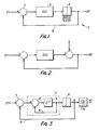
- a D/A converter 2 comprises combiner means 4, which may take the form of an X-bit adder, for receiving a digital input Dl.
- the combiner means 4 is connected to digital controller means 6, the output of which is connected to a one bit quantiser in the form of digital slicer means 8.
- Feedback means is provided, in the form of a digital feedback control loop 10, between the output of the digital slicer 8 and the combiner means 4.
- the D/A converter shown in Figure 1 limit cycles to produce an output bit stream Do which has a mean mark to space ratio proportional to the digital input word.
- This output bit stream may be analogue filtered to a voltage which is directly proportional to the input word.
- Figure 2 illustrates the noise model of the D/A converter 2 where Q is the quantisation error of the one bit quantiser 8 shown in Figure 1.
- the error, or noise term Eq(z) of the D/A converter 2 may be expressed as:
- the D/A converter 2 may be analysed as follows: Let: then the gain of the digital controller means 6:
- equation (3) determines the open loop gain of the D/A converter and it is maximised by choosing the fastest closed loop response to a given type of input; such as by the use of an optimum controller for the digital controller means 6, the optimum value for G(z) occurring when the closed loop exhibits a "Deadbeat" response.
- "Deadbeat" response is described in detail in section 10.8 of "Digital Control Systems” by Benjamin C. Kuo published by Holt/Saunders International Editions, the subject matter of which is incorporated herein by reference.
- Increasing the type of loop allows greater reduction of Eq (the error or noise term of the D/A converter 2), for a given bandwidth F L of the analogue filter means at a clock rate F s of the D/A converter 2.
- Table A shows the required controller G(z) for maximum reduction of the noise term Eq for three types of loop.
- Suitable digital controllers for use in the analogue to digital converter 2 of which the type 1, 2 and 3 optimum controllers referred to in Table A are merely illustrative, are described in detail in Chapter 17 of "Feedback Control System Analysis and Synthesis" by J.J. D'Azzo and C.H. Houpis published by McGraw Hill, the subject matter of which is incorporated herein by reference.
- the type 1 digital controller comprises summing means 12 in combination with delay means 14 and a feedback loop 16 connecting the output of the delay means 14 to the summing means 12.
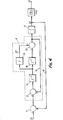
- the type 2 digital controller shown in Figure 4 includes a second delay means 18, further summing means 20 and a feed forward loop 22 including a multiplier 24.
- the type 3 digital controller shown in Figure 5 includes a third delay means 26 and a second feed forward loop 28 including a multiplier 30.
- the delay means 14, 18 and 26 used in these controllers may comprise D-type flip-flops.
- the analogue filter used at the output of the D/A converter 2 must therefore have an order greater than this to realise the possible D/A resolution. It can be seen from this expression that choosing a filter having a Butterworth characteristic will only result in a loss of approximately 2 dB in resolution when compared to an ideal filter.
- This output filter can either be a low noise active filter or a passive LC type of filter.
- the settling time of the analogue output filter can be expressed as Ln2 N0UT 21T FL Substituting the above value in this expression gives a settling time of approximately 19/uS at 17 bits resolution.
- the present invention provides extremely linear and fairly fast D/A converters which can be realised cheaply and easily and having a performance which rivals conventional ladder network types.
- a D/A converter 2 in accordance with the present invention and incorporating a Type 3 digital controller may be realised on any integrated circuit gate array and provides a programmable, robust and linear D/A converter with speeds and accuracy matching conventional high precision open loop converters.
- D/A converters in accordance with the present invention may be utilised in any application where high resolution is required such as, for example, high resolution graphics or high quality audio equipment.
Landscapes
- Engineering & Computer Science (AREA)
- Theoretical Computer Science (AREA)
- Analogue/Digital Conversion (AREA)
Applications Claiming Priority (2)
| Application Number | Priority Date | Filing Date | Title |
|---|---|---|---|
| GB848427325A GB8427325D0 (en) | 1984-10-29 | 1984-10-29 | Digital to analogue conversion |
| GB8427325 | 1984-10-29 |
Publications (2)
| Publication Number | Publication Date |
|---|---|
| EP0180461A2 true EP0180461A2 (fr) | 1986-05-07 |
| EP0180461A3 EP0180461A3 (fr) | 1989-03-29 |
Family
ID=10568917
Family Applications (1)
| Application Number | Title | Priority Date | Filing Date |
|---|---|---|---|
| EP85307833A Withdrawn EP0180461A3 (fr) | 1984-10-29 | 1985-10-29 | Convertisseurs numériques-analogiques |
Country Status (2)
| Country | Link |
|---|---|
| EP (1) | EP0180461A3 (fr) |
| GB (2) | GB8427325D0 (fr) |
Cited By (2)
| Publication number | Priority date | Publication date | Assignee | Title |
|---|---|---|---|---|
| EP0271166A2 (fr) * | 1986-12-10 | 1988-06-15 | Philips Patentverwaltung GmbH | Agencement de circuit numérique de réduction du bruit de quantification |
| EP0559732A1 (fr) * | 1990-11-27 | 1993-09-15 | Gordon M Jacobs | Convertisseur de donnees numeriques. |
Families Citing this family (1)
| Publication number | Priority date | Publication date | Assignee | Title |
|---|---|---|---|---|
| GB2270595B (en) * | 1992-09-09 | 1995-12-06 | Guy De Warrenne Bruce Adams | An audio system |
Citations (2)
| Publication number | Priority date | Publication date | Assignee | Title |
|---|---|---|---|---|
| US4209773A (en) * | 1976-12-01 | 1980-06-24 | The Post Office | Code converters |
| GB2107949A (en) * | 1981-10-15 | 1983-05-05 | Standard Telephones Cables Ltd | Digital decoder |
Family Cites Families (1)
| Publication number | Priority date | Publication date | Assignee | Title |
|---|---|---|---|---|
| DE3021012C2 (de) * | 1980-06-03 | 1985-08-22 | ANT Nachrichtentechnik GmbH, 7150 Backnang | Verallgemeinertes interpolativers Verfahren zur Digital-Analog-Umsetzung von PCM Signalen |
-
1984
- 1984-10-29 GB GB848427325A patent/GB8427325D0/en active Pending
-
1985
- 1985-10-29 EP EP85307833A patent/EP0180461A3/fr not_active Withdrawn
- 1985-10-29 GB GB08526643A patent/GB2166614A/en not_active Withdrawn
Patent Citations (2)
| Publication number | Priority date | Publication date | Assignee | Title |
|---|---|---|---|---|
| US4209773A (en) * | 1976-12-01 | 1980-06-24 | The Post Office | Code converters |
| GB2107949A (en) * | 1981-10-15 | 1983-05-05 | Standard Telephones Cables Ltd | Digital decoder |
Cited By (4)
| Publication number | Priority date | Publication date | Assignee | Title |
|---|---|---|---|---|
| EP0271166A2 (fr) * | 1986-12-10 | 1988-06-15 | Philips Patentverwaltung GmbH | Agencement de circuit numérique de réduction du bruit de quantification |
| EP0271166A3 (fr) * | 1986-12-10 | 1991-06-26 | Philips Patentverwaltung GmbH | Agencement de circuit numérique de réduction du bruit de quantification |
| EP0559732A1 (fr) * | 1990-11-27 | 1993-09-15 | Gordon M Jacobs | Convertisseur de donnees numeriques. |
| EP0559732A4 (en) * | 1990-11-27 | 1993-12-15 | Gordon M. Jacobs | Digital data converter |
Also Published As
| Publication number | Publication date |
|---|---|
| EP0180461A3 (fr) | 1989-03-29 |
| GB8526643D0 (en) | 1985-12-04 |
| GB8427325D0 (en) | 1984-12-05 |
| GB2166614A (en) | 1986-05-08 |
Similar Documents
| Publication | Publication Date | Title |
|---|---|---|
| US7460046B2 (en) | Sigma-delta modulators | |
| JP2543095B2 (ja) | オ―バ―サンプリング型d/a変換器 | |
| EP0586021B1 (fr) | Circuit numérique de formation de bruit | |
| DE69927084T2 (de) | Sigma-delta Modulator und Modulationsverfahren | |
| EP0454407B1 (fr) | Convertisseur analogique-numérique de type sigma-delta à plusieurs étages | |
| EP0199745B1 (fr) | Convertisseur analogique numerique | |
| US4872129A (en) | Digital decimation filter | |
| CA1175945A (fr) | Procede interpolateur generalise pour la conversion numerique-analogique des signaux mic | |
| EP2346167A1 (fr) | Résonateur et convertisseur a/n de suréchantillonnage | |
| DE102008025367B4 (de) | Filter mit kapazitiver Vorwärtskopplung | |
| US4843390A (en) | Oversampled A/D converter having digital error correction | |
| DE602005001311T2 (de) | Schaltverstärker | |
| KR100302156B1 (ko) | 데시메이션필터 | |
| EP0461282B1 (fr) | Convertisseur analogique numérique à suréchantillonnage avec filtrage de bruit en technique de capacités commutée | |
| US4789862A (en) | Analogue to digital converters | |
| JP2002506603A (ja) | 多項式補間を用いたサンプルレート変換器 | |
| EP0476973A1 (fr) | Circuit formeur de bruit | |
| EP0388958A2 (fr) | Circuit de compensation de gain/phase pour utilisation dans un système de contrôle d'asservissement d'un appareil à disque optique | |
| EP0180461A2 (fr) | Convertisseurs numériques-analogiques | |
| CN117560010A (zh) | 模数转换系统 | |
| US5089981A (en) | Hybrid form digital filter | |
| US6570512B1 (en) | Circuit configuration for quantization of digital signals and for filtering quantization noise | |
| EP0229073B1 (fr) | Ameliorations relatives a des convertisseurs analogiques-numeriques | |
| US7423566B2 (en) | Sigma-delta modulator using a passive filter | |
| EP0680151A1 (fr) | Dispositif de conversion analogique-numérique pour signaux différentials à basses fréquences et basses amplitudes |
Legal Events
| Date | Code | Title | Description |
|---|---|---|---|
| PUAI | Public reference made under article 153(3) epc to a published international application that has entered the european phase |
Free format text: ORIGINAL CODE: 0009012 |
|
| AK | Designated contracting states |
Kind code of ref document: A2 Designated state(s): AT BE CH DE FR IT LI LU NL SE |
|
| PUAL | Search report despatched |
Free format text: ORIGINAL CODE: 0009013 |
|
| AK | Designated contracting states |
Kind code of ref document: A3 Designated state(s): AT BE CH DE FR IT LI LU NL SE |
|
| STAA | Information on the status of an ep patent application or granted ep patent |
Free format text: STATUS: THE APPLICATION IS DEEMED TO BE WITHDRAWN |
|
| 18D | Application deemed to be withdrawn |
Effective date: 19890930 |
|
| RIN1 | Information on inventor provided before grant (corrected) |
Inventor name: JACKSON, THOMAS |