EP0180020A2 - Dispositif de gravure par plasma - Google Patents
Dispositif de gravure par plasma Download PDFInfo
- Publication number
- EP0180020A2 EP0180020A2 EP85111747A EP85111747A EP0180020A2 EP 0180020 A2 EP0180020 A2 EP 0180020A2 EP 85111747 A EP85111747 A EP 85111747A EP 85111747 A EP85111747 A EP 85111747A EP 0180020 A2 EP0180020 A2 EP 0180020A2
- Authority
- EP
- European Patent Office
- Prior art keywords
- plasma
- microwave
- gas
- etched
- flowing
- Prior art date
- Legal status (The legal status is an assumption and is not a legal conclusion. Google has not performed a legal analysis and makes no representation as to the accuracy of the status listed.)
- Ceased
Links
Images

Classifications
-
- H—ELECTRICITY
- H01—ELECTRIC ELEMENTS
- H01J—ELECTRIC DISCHARGE TUBES OR DISCHARGE LAMPS
- H01J37/00—Discharge tubes with provision for introducing objects or material to be exposed to the discharge, e.g. for the purpose of examination or processing thereof
- H01J37/32—Gas-filled discharge tubes
- H01J37/32009—Arrangements for generation of plasma specially adapted for examination or treatment of objects, e.g. plasma sources
- H01J37/32357—Generation remote from the workpiece, e.g. down-stream
-
- H—ELECTRICITY
- H05—ELECTRIC TECHNIQUES NOT OTHERWISE PROVIDED FOR
- H05H—PLASMA TECHNIQUE; PRODUCTION OF ACCELERATED ELECTRICALLY-CHARGED PARTICLES OR OF NEUTRONS; PRODUCTION OR ACCELERATION OF NEUTRAL MOLECULAR OR ATOMIC BEAMS
- H05H1/00—Generating plasma; Handling plasma
- H05H1/24—Generating plasma
- H05H1/46—Generating plasma using applied electromagnetic fields, e.g. high frequency or microwave energy
Definitions
- This invention relates to dry chemical etching systems and methods for use in fabricating integrated circuits and the like and more particularly it relates to a plasma etching system and method having both microwave and radio frequency (RF) excitation.
- RF radio frequency
- Microwave plasma reactors are used in the semiconductor industry to perform both deposition and etching steps. With this method, a suitable gas or combination of gases is excited with microwave energy to form a plasma containing chemically reactive species such as ions, electrons and radicals. The microwave plasma is slowly flowed against the surface being treated, where the reactive species cause chemical reactions to occur which result in either material deposition or material removal (etching).
- a suitable gas or combination of gases is excited with microwave energy to form a plasma containing chemically reactive species such as ions, electrons and radicals.
- the microwave plasma is slowly flowed against the surface being treated, where the reactive species cause chemical reactions to occur which result in either material deposition or material removal (etching).
- Radio frequency plasma reactors are also used in the semiconductor industry for both etching and deposition.
- a suitable gas or combination of gases is excited by a high frequency electrical discharge rather than by microwave energy.
- RF excitation a plasma is also produced which contains ions, electrons and radicals.
- the ions, electrons and radicals in the RF excited plasma are much less chemically excited than in the microwave plasma.
- ion bombardment of the surface being treated occurs with an RF excited plasma due to the electric potential of the plasma relative to the surface being treated.
- RF excited plasmas tend to etch anisotroplically while microwave excited plasmas tend to etch isotropically.
- Etching systems have also been described in the prior art which use both a microwave plasma and an RF plasma. Examples of such systems may be found, for example, in U.S. Patents 4,136,791; 4,384,933 and 4,282,267.
- the invention provides apparatus for etching a material surface with a plasma, comprising: a reaction chamber having an internal electrode for supporting the material to be etched; means for flowing a gas against the material surface to be etched: means for exciting said flowing gas with microwave energy to form a flowing microwave plasma, said flowing microwave plasma being continuously excited by microwave energy as it flows against said material surface to be etched; and a high frequency power source connected to said electrode for simultaneously exciting said microwave plasma flowing against said material surface to be etched with a radio frequency electric field, said radio frequency excitation enhancing the etching rate of said microwave plasma and making the etching effect of said microwave plasma more anisotropic.
- the invention also provides a method for etching a material surface with a plasma, comprising the steps of: forming a microwave plasma; flowing the microwave plasma against the material surface to be etched, the microwave plasma being continuously excited with microwave energy while it flows against said surface to be etched; and simultaneously exciting said microwave plasma flowing against said surface to be etched with a radio frequency electric field, said radio frequency excitation enhancing the etching rate of said microwave plasma and making the etching effect of said microwave plasma more anisotropic.
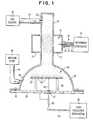
- a microwave cavity 10 defined by metallic walls 12 receives microwave power from microwave generator 14 via a conventional microwave waveguide 16 comprising a central electrical conductor 18 spaced from a concentric conductive tube 20 by dielectric material 22. Passing through microwave cavity 10 is a gas confining tube 24 closed at one end except for a gas inlet opening 25 and connected at the other end to a reaction chamber 26.
- the walls 28 of reaction chamber 26 and tube 24 are composed of a material which is permeable to the microwave frequency at which generator 14 is driving cavity 10.
- the size of the hole through which tube 24 exits cavity 10 is sufficiently large and-the distance between the cavity 10 and chamber 26 sufficiently small that microwaves will leak out of cavity 10 and propagate downward to significantly stimulate with microwaves not only the region within tube 24 which is within cavity 10 but also the region within tube 24 below cavity 10 and the region of chamber 26 between electrode 30 and cavity 10. Since the walls 28 of reaction chamber 26 and tube 24 will contain a plasma, the material selected for the tube 24 and walls 28 also must be able to tolerate the expected high temperature.
- a suitable material for the walls 28 and tube 24 is quartz, for example.
- a suitable gas or a mixture of gases from source 32 enters tube 24 via gas hose or tubing 34 at the end of tube 24 remote from the reaction chamber 26 and flows down tube 24 and into chamber 26.
- Chamber 26 comprises upper walls 28 and a support base 36 sealed to walls 28 via 0-ring 38.
- Chamber 26 also contains a gas exit opening 40 connected via a tube or hose 42 to a vacuum pump 44.
- Vacuum pump 44 in cooperation with gas source 32 establish a gas flow which travels down tube 24 and strikes electrode 30 much as if electrode 30 were a gas flow baffle.
- the workpiece or workpieces sought to be etched are placed on top of electrode 30 with the material side or surface to be etched facing upward towards the gas flow from tube 24. In Fig. 1, the workpieces sought to be etched are silicon wafers 46.
- Electrode 30 is connected via a conductor 48 to a high frequency generator 50.
- Conductor 48 has shielding 52 electrically connected to base 36, which is also conductive.
- a grommet or plug 54 insulates conductor 48 from electrical contact with base 36.
- Electrode 30 is both supported from base 36 and electrically insulated therefrom by legs 56.
- a gas suitable for forming the desired plasma flows into tube 24 from gas source 32.
- gases for example, include many of the halogens, halocarbons, rare gases, and the like, including for example: 0 2 , N 2 , H 2' CF 4 , C1 2 , SF 6 , etc.
- the gas pressure is moderately low, such as 100 mTorr.
- the plasma also extends within tube 24 to some extent upward beyond the microwave cavity 10 due to diffusion of gaseous constituents and leakage of the microwaves upward through the top hole in the microwave cavity.
- the microwave plasma also extends downward into chamber 26 and covers electrode 30 and anything on electrode 30. As described earlier, microwave stimulation of the plasma extends all the way down to electrode 30. As will become apparent from an experiment to be described below, since the microwave plasma directly contacts the workpieces 46, etching of the workpieces will occur (assuming the surface of the workpieces are capable of being etched by the type of microwave plasma formed) even without any RF excitation of electrode 30, though at a much slower rate and in an isotropic fashion.
- radio frequency (RF) electrical power is simultaneously applied to electrode 30.
- RF radio frequency
- the RF power supplied to electrode 30 alone would create a plasma.
- Such an RF excited plasma is often called an RIE (reactive ion etching) plasma.
- Fig. 2 graphically illustrates some experimental results obtained with the apparatus shown in Fig. 1.
- the experiment was conducted using a 6.25 cm. graphite wafer as a workpiece substrate upon which a conventional resist was deposited (Shipley AZ 1350J resist). The rate at which the resist was etched by an oxygen plasma was then measured under various conditions. The measured etch rate is plotted in Fig. -2 against the power supplied by the microwave source at 2.54 GHz.
- Curve 60 connects the experimental data points obtained when the high frequency generator 50 was supplying no power at all to the plasma (generator 50 was turned off).
- Curve 62 connects the experimental data points obtained when the high frequency generator was supplying 5 watts of power to the plasma at 13.56 MHz.
- the etch rate was 100 Angstroms per minute at 5 watts of applied RF power.
- the microwave source 14 alone was used to form the plasma (data point 66) the etch rate was 2000 Angstroms per minute at 50 watts of applied microwave power.
- the plasma was excited simultaneously with 5 watts of RF power and 50 watts of microwave power (data point 68), the etch rate was 8000 Angstroms per minute, about 4 times the linear sum of the two individual etch rates.
- the side wall profile of the etched resist was vertical (perpendicular to the electrode) when the plasma was stimulated by only RF power and severely undercut (the bottom of etched grooves were wider than the top) when the plasma was stimulated entirely by microwaves. When both microwaves and RF power were used to stimulate the plasma, the side wall profile was intermediate between the two (i.e. slightly undercut).
Landscapes
- Physics & Mathematics (AREA)
- Engineering & Computer Science (AREA)
- Plasma & Fusion (AREA)
- Electromagnetism (AREA)
- Spectroscopy & Molecular Physics (AREA)
- Chemical & Material Sciences (AREA)
- Analytical Chemistry (AREA)
- Drying Of Semiconductors (AREA)
- ing And Chemical Polishing (AREA)
Applications Claiming Priority (2)
| Application Number | Priority Date | Filing Date | Title |
|---|---|---|---|
| US06/665,696 US4581100A (en) | 1984-10-29 | 1984-10-29 | Mixed excitation plasma etching system |
| US665696 | 1996-06-18 |
Publications (2)
| Publication Number | Publication Date |
|---|---|
| EP0180020A2 true EP0180020A2 (fr) | 1986-05-07 |
| EP0180020A3 EP0180020A3 (fr) | 1987-10-07 |
Family
ID=24671202
Family Applications (1)
| Application Number | Title | Priority Date | Filing Date |
|---|---|---|---|
| EP85111747A Ceased EP0180020A3 (fr) | 1984-10-29 | 1985-09-17 | Dispositif de gravure par plasma |
Country Status (3)
| Country | Link |
|---|---|
| US (1) | US4581100A (fr) |
| EP (1) | EP0180020A3 (fr) |
| JP (1) | JPS61107730A (fr) |
Cited By (9)
| Publication number | Priority date | Publication date | Assignee | Title |
|---|---|---|---|---|
| EP0216603A2 (fr) * | 1985-09-17 | 1987-04-01 | Machine Technology Inc. | Appareil micro-onde générateur de post-luminescences plasmatiques |
| EP0261347A1 (fr) * | 1986-08-27 | 1988-03-30 | International Business Machines Corporation | Dispositif de pulvérisation |
| EP0270667A1 (fr) * | 1986-06-12 | 1988-06-15 | Univ Michigan State | Appareil a micro-ondes a double plasma et procede de traitement de surfaces. |
| EP0277460A1 (fr) * | 1986-12-16 | 1988-08-10 | Plasma-Seven S.A. | Procédé pour la restitution d'une structure métallique dans une surface dégradée d'un objet en métal, application de ce procédé et dispositif pour la mise en oeuvre du procédé |
| FR2616030A1 (fr) * | 1987-06-01 | 1988-12-02 | Commissariat Energie Atomique | Procede de gravure ou de depot par plasma et dispositif pour la mise en oeuvre du procede |
| US4818359A (en) * | 1986-08-27 | 1989-04-04 | International Business Machines Corporation | Low contamination RF sputter deposition apparatus |
| EP0334638A1 (fr) * | 1988-03-22 | 1989-09-27 | Semiconductor Energy Laboratory Co., Ltd. | Formation de films minces |
| FR2631199A1 (fr) * | 1988-05-09 | 1989-11-10 | Centre Nat Rech Scient | Reacteur a plasma |
| EP0343017A2 (fr) * | 1988-05-20 | 1989-11-23 | Nec Corporation | Appareil de gravure ionique réactive |
Families Citing this family (38)
| Publication number | Priority date | Publication date | Assignee | Title |
|---|---|---|---|---|
| US6784033B1 (en) | 1984-02-15 | 2004-08-31 | Semiconductor Energy Laboratory Co., Ltd. | Method for the manufacture of an insulated gate field effect semiconductor device |
| US5780313A (en) | 1985-02-14 | 1998-07-14 | Semiconductor Energy Laboratory Co., Ltd. | Method of fabricating semiconductor device |
| JPH0824114B2 (ja) * | 1984-11-09 | 1996-03-06 | 株式会社日立製作所 | プラズマエッチング方法 |
| JPH0752718B2 (ja) * | 1984-11-26 | 1995-06-05 | 株式会社半導体エネルギー研究所 | 薄膜形成方法 |
| US6786997B1 (en) | 1984-11-26 | 2004-09-07 | Semiconductor Energy Laboratory Co., Ltd. | Plasma processing apparatus |
| JPS61222534A (ja) * | 1985-03-28 | 1986-10-03 | Anelva Corp | 表面処理方法および装置 |
| US6230650B1 (en) | 1985-10-14 | 2001-05-15 | Semiconductor Energy Laboratory Co., Ltd. | Microwave enhanced CVD system under magnetic field |
| US6673722B1 (en) | 1985-10-14 | 2004-01-06 | Semiconductor Energy Laboratory Co., Ltd. | Microwave enhanced CVD system under magnetic field |
| US5427824A (en) * | 1986-09-09 | 1995-06-27 | Semiconductor Energy Laboratory Co., Ltd. | CVD apparatus |
| KR910003742B1 (ko) * | 1986-09-09 | 1991-06-10 | 세미콘덕터 에너지 라보라터리 캄파니 리미티드 | Cvd장치 |
| JPS6423364A (en) * | 1987-07-20 | 1989-01-26 | Mitsubishi Electric Corp | Document editing device |
| JPS6423536A (en) * | 1987-07-20 | 1989-01-26 | Hitachi Ltd | Sputter-etching device |
| US4831244A (en) * | 1987-10-01 | 1989-05-16 | Polaroid Corporation | Optical record cards |
| US4778561A (en) * | 1987-10-30 | 1988-10-18 | Veeco Instruments, Inc. | Electron cyclotron resonance plasma source |
| GB2212974B (en) * | 1987-11-25 | 1992-02-12 | Fuji Electric Co Ltd | Plasma processing apparatus |
| NL8702875A (nl) * | 1987-12-01 | 1989-07-03 | Philips Nv | Werkwijze voor het vervaardigen van een halfgeleiderinrichting waarbij fotolak op een laag van siliciumoxide op een halfgeleidersubstraat wordt verwijderd. |
| KR920003431B1 (ko) * | 1988-02-05 | 1992-05-01 | 가부시끼가이샤 한도다이 에네르기 겐뀨쇼 | 플라즈마 처리 방법 및 장치 |
| JP2768685B2 (ja) * | 1988-03-28 | 1998-06-25 | 株式会社東芝 | 半導体装置の製造方法及びその装置 |
| US4893584A (en) * | 1988-03-29 | 1990-01-16 | Energy Conversion Devices, Inc. | Large area microwave plasma apparatus |
| JPH0216732A (ja) * | 1988-07-05 | 1990-01-19 | Mitsubishi Electric Corp | プラズマ反応装置 |
| US5202095A (en) * | 1988-12-27 | 1993-04-13 | Matsushita Electric Industrial Co., Ltd. | Microwave plasma processor |
| US4888088A (en) * | 1989-03-06 | 1989-12-19 | Tegal Corporation | Ignitor for a microwave sustained plasma |
| US4943345A (en) * | 1989-03-23 | 1990-07-24 | Board Of Trustees Operating Michigan State University | Plasma reactor apparatus and method for treating a substrate |
| US5556501A (en) * | 1989-10-03 | 1996-09-17 | Applied Materials, Inc. | Silicon scavenger in an inductively coupled RF plasma reactor |
| US6068784A (en) * | 1989-10-03 | 2000-05-30 | Applied Materials, Inc. | Process used in an RF coupled plasma reactor |
| US6251792B1 (en) | 1990-07-31 | 2001-06-26 | Applied Materials, Inc. | Plasma etch processes |
| US6444137B1 (en) | 1990-07-31 | 2002-09-03 | Applied Materials, Inc. | Method for processing substrates using gaseous silicon scavenger |
| US5234565A (en) * | 1990-09-20 | 1993-08-10 | Matsushita Electric Industrial Co., Ltd. | Microwave plasma source |
| US5888414A (en) * | 1991-06-27 | 1999-03-30 | Applied Materials, Inc. | Plasma reactor and processes using RF inductive coupling and scavenger temperature control |
| US6518195B1 (en) | 1991-06-27 | 2003-02-11 | Applied Materials, Inc. | Plasma reactor using inductive RF coupling, and processes |
| US5480533A (en) * | 1991-08-09 | 1996-01-02 | Matsushita Electric Industrial Co., Ltd. | Microwave plasma source |
| JP2625072B2 (ja) * | 1992-09-08 | 1997-06-25 | アプライド マテリアルズ インコーポレイテッド | 電磁rf結合を用いたプラズマ反応装置及びその方法 |
| US5662770A (en) * | 1993-04-16 | 1997-09-02 | Micron Technology, Inc. | Method and apparatus for improving etch uniformity in remote source plasma reactors with powered wafer chucks |
| JPH0936103A (ja) * | 1995-07-18 | 1997-02-07 | Ulvac Japan Ltd | 半導体ウェハのエッチング及びレジスト除去のための方法並びに装置 |
| US6015761A (en) * | 1996-06-26 | 2000-01-18 | Applied Materials, Inc. | Microwave-activated etching of dielectric layers |
| US5795831A (en) * | 1996-10-16 | 1998-08-18 | Ulvac Technologies, Inc. | Cold processes for cleaning and stripping photoresist from surfaces of semiconductor wafers |
| FR2862070B1 (fr) * | 2003-11-06 | 2006-02-03 | Vector Advanced Surface Techno | Installation de traitement en continu de la surface d'objets et procede pour la mise en oeuvre de ce traitement |
| JP2018127369A (ja) * | 2017-02-06 | 2018-08-16 | 東京エレクトロン株式会社 | グラフェンの異方性エッチング方法 |
Citations (4)
| Publication number | Priority date | Publication date | Assignee | Title |
|---|---|---|---|---|
| GB2056919A (en) * | 1979-08-22 | 1981-03-25 | Onera (Off Nat Aerospatiale) | Chemical dry etching of integrated circuits |
| US4298419A (en) * | 1979-07-13 | 1981-11-03 | Hitachi, Ltd. | Dry etching apparatus |
| US4401054A (en) * | 1980-05-02 | 1983-08-30 | Nippon Telegraph & Telephone Public Corporation | Plasma deposition apparatus |
| EP0140294B1 (fr) * | 1983-10-19 | 1990-04-25 | Hitachi, Ltd. | Méthode de traitement par plasma et appareil pour la mise en oeuvre de cette méthode |
Family Cites Families (2)
| Publication number | Priority date | Publication date | Assignee | Title |
|---|---|---|---|---|
| JPS5940227B2 (ja) * | 1980-06-24 | 1984-09-28 | 富士通株式会社 | リアクティブスパッタリング方法 |
| JPS6015931A (ja) * | 1983-07-07 | 1985-01-26 | Fujitsu Ltd | 反応性イオンエツチング方法 |
-
1984
- 1984-10-29 US US06/665,696 patent/US4581100A/en not_active Expired - Fee Related
-
1985
- 1985-08-09 JP JP60174446A patent/JPS61107730A/ja active Pending
- 1985-09-17 EP EP85111747A patent/EP0180020A3/fr not_active Ceased
Patent Citations (4)
| Publication number | Priority date | Publication date | Assignee | Title |
|---|---|---|---|---|
| US4298419A (en) * | 1979-07-13 | 1981-11-03 | Hitachi, Ltd. | Dry etching apparatus |
| GB2056919A (en) * | 1979-08-22 | 1981-03-25 | Onera (Off Nat Aerospatiale) | Chemical dry etching of integrated circuits |
| US4401054A (en) * | 1980-05-02 | 1983-08-30 | Nippon Telegraph & Telephone Public Corporation | Plasma deposition apparatus |
| EP0140294B1 (fr) * | 1983-10-19 | 1990-04-25 | Hitachi, Ltd. | Méthode de traitement par plasma et appareil pour la mise en oeuvre de cette méthode |
Non-Patent Citations (1)
| Title |
|---|
| JOURNAL OF VACUUM SCIENCE AND TECHNOLOGY B, vol. 3, no. 4, July-August 1985, pages 1025-1034, American Vacuum Society, Woodbury, New York, US; K. SUZUKI et al.: "Radio-frequency biased microwave plasma etching technique: a method to increase SiO2 etch rate" * |
Cited By (16)
| Publication number | Priority date | Publication date | Assignee | Title |
|---|---|---|---|---|
| EP0216603A3 (fr) * | 1985-09-17 | 1987-12-23 | Machine Technology Inc. | Appareil micro-onde générateur de post-luminescences plasmatiques |
| EP0216603A2 (fr) * | 1985-09-17 | 1987-04-01 | Machine Technology Inc. | Appareil micro-onde générateur de post-luminescences plasmatiques |
| EP0270667A1 (fr) * | 1986-06-12 | 1988-06-15 | Univ Michigan State | Appareil a micro-ondes a double plasma et procede de traitement de surfaces. |
| EP0270667B1 (fr) * | 1986-06-12 | 1992-01-15 | Michigan State University | Appareil a micro-ondes a double plasma et procede de traitement de surfaces |
| EP0261347A1 (fr) * | 1986-08-27 | 1988-03-30 | International Business Machines Corporation | Dispositif de pulvérisation |
| US4818359A (en) * | 1986-08-27 | 1989-04-04 | International Business Machines Corporation | Low contamination RF sputter deposition apparatus |
| EP0277460A1 (fr) * | 1986-12-16 | 1988-08-10 | Plasma-Seven S.A. | Procédé pour la restitution d'une structure métallique dans une surface dégradée d'un objet en métal, application de ce procédé et dispositif pour la mise en oeuvre du procédé |
| US5047115A (en) * | 1987-06-01 | 1991-09-10 | Commissariat A L'energie Atomique | Process for etching by gas plasma |
| FR2616030A1 (fr) * | 1987-06-01 | 1988-12-02 | Commissariat Energie Atomique | Procede de gravure ou de depot par plasma et dispositif pour la mise en oeuvre du procede |
| WO1988009830A1 (fr) * | 1987-06-01 | 1988-12-15 | Commissariat A L'energie Atomique | Procede de gravure par plasma gazeux |
| EP0334638A1 (fr) * | 1988-03-22 | 1989-09-27 | Semiconductor Energy Laboratory Co., Ltd. | Formation de films minces |
| EP0346168A1 (fr) * | 1988-05-09 | 1989-12-13 | Centre National De La Recherche Scientifique (Cnrs) | Réacteur à plasma |
| WO1989011206A1 (fr) * | 1988-05-09 | 1989-11-16 | Centre National De La Recherche Scientifique (Cnrs | Reacteur a plasma |
| FR2631199A1 (fr) * | 1988-05-09 | 1989-11-10 | Centre Nat Rech Scient | Reacteur a plasma |
| EP0343017A2 (fr) * | 1988-05-20 | 1989-11-23 | Nec Corporation | Appareil de gravure ionique réactive |
| EP0343017A3 (fr) * | 1988-05-20 | 1990-05-23 | Nec Corporation | Appareil de gravure ionique réactive |
Also Published As
| Publication number | Publication date |
|---|---|
| EP0180020A3 (fr) | 1987-10-07 |
| JPS61107730A (ja) | 1986-05-26 |
| US4581100A (en) | 1986-04-08 |
Similar Documents
| Publication | Publication Date | Title |
|---|---|---|
| US4581100A (en) | Mixed excitation plasma etching system | |
| JP4794449B2 (ja) | ナローギャップ容量結合リアクタのrfパルシング技術 | |
| US4585668A (en) | Method for treating a surface with a microwave or UHF plasma and improved apparatus | |
| US4464223A (en) | Plasma reactor apparatus and method | |
| EP0035565B1 (fr) | Procedes et appareil de production de plasmas | |
| US4630566A (en) | Microwave or UHF plasma improved apparatus | |
| US7396431B2 (en) | Plasma processing system for treating a substrate | |
| US5607542A (en) | Inductively enhanced reactive ion etching | |
| KR101689916B1 (ko) | 중력에 의한 가스 확산 분리(gigds) 기술에 의해 제어되는 플라즈마 발생 시스템 | |
| US4148705A (en) | Gas plasma reactor and process | |
| US8968588B2 (en) | Low electron temperature microwave surface-wave plasma (SWP) processing method and apparatus | |
| US20100003827A1 (en) | Method and device for etching a substrate by means of plasma | |
| WO2001046492A1 (fr) | Procede et systeme reduisant les dommages subis par les substrats lors de traitements au plasma par source resonante | |
| KR20080048541A (ko) | 기판에서 불소계 폴리머를 제거하기 위한 장치 및 그를위한 방법 | |
| JPS61136229A (ja) | ドライエツチング装置 | |
| JPH09289193A (ja) | プラズマ発生装置及びその方法、並びにプラズマ処理装置及びその方法 | |
| US5783100A (en) | Method of high density plasma etching for semiconductor manufacture | |
| US7584714B2 (en) | Method and system for improving coupling between a surface wave plasma source and a plasma space | |
| JPS6136589B2 (fr) | ||
| JP3042208B2 (ja) | マイクロ波プラズマ処理装置 | |
| KR100255088B1 (ko) | 플라즈마처리장치 | |
| US6037267A (en) | Method of etching metallic film for semiconductor devices | |
| JPH05283196A (ja) | プラズマ装置および該装置の使用方法 | |
| JPH11191554A (ja) | プラズマ処理装置およびプラズマ処理方法 | |
| JPH08170181A (ja) | ドライエッチング方法 |
Legal Events
| Date | Code | Title | Description |
|---|---|---|---|
| PUAI | Public reference made under article 153(3) epc to a published international application that has entered the european phase |
Free format text: ORIGINAL CODE: 0009012 |
|
| AK | Designated contracting states |
Kind code of ref document: A2 Designated state(s): DE FR GB |
|
| 17P | Request for examination filed |
Effective date: 19860819 |
|
| PUAL | Search report despatched |
Free format text: ORIGINAL CODE: 0009013 |
|
| AK | Designated contracting states |
Kind code of ref document: A3 Designated state(s): DE FR GB |
|
| 17Q | First examination report despatched |
Effective date: 19880715 |
|
| STAA | Information on the status of an ep patent application or granted ep patent |
Free format text: STATUS: THE APPLICATION HAS BEEN REFUSED |
|
| 18R | Application refused |
Effective date: 19901012 |
|
| APAF | Appeal reference modified |
Free format text: ORIGINAL CODE: EPIDOSCREFNE |
|
| RIN1 | Information on inventor provided before grant (corrected) |
Inventor name: ROBINSON, BENNETT Inventor name: HATZAKIS, MICHAEL Inventor name: PARASZCZAK, JURI ROSTYSLAV |