EP0179852B1 - Dotierte und nicht-dotierte, einkristaline, mehrschichtige strukturen - Google Patents
Dotierte und nicht-dotierte, einkristaline, mehrschichtige strukturen Download PDFInfo
- Publication number
- EP0179852B1 EP0179852B1 EP85902246A EP85902246A EP0179852B1 EP 0179852 B1 EP0179852 B1 EP 0179852B1 EP 85902246 A EP85902246 A EP 85902246A EP 85902246 A EP85902246 A EP 85902246A EP 0179852 B1 EP0179852 B1 EP 0179852B1
- Authority
- EP
- European Patent Office
- Prior art keywords
- layer
- silver thiogallate
- electro
- layers
- thiogallate
- Prior art date
- Legal status (The legal status is an assumption and is not a legal conclusion. Google has not performed a legal analysis and makes no representation as to the accuracy of the status listed.)
- Expired - Lifetime
Links
- 239000013078 crystal Substances 0.000 title claims abstract description 69
- BQCADISMDOOEFD-UHFFFAOYSA-N Silver Chemical compound [Ag] BQCADISMDOOEFD-UHFFFAOYSA-N 0.000 claims abstract description 90
- 229910052709 silver Inorganic materials 0.000 claims abstract description 90
- 239000004332 silver Substances 0.000 claims abstract description 90
- 239000002019 doping agent Substances 0.000 claims abstract description 28
- 239000000203 mixture Substances 0.000 claims abstract description 25
- 239000000463 material Substances 0.000 claims abstract description 23
- 239000000758 substrate Substances 0.000 claims abstract description 23
- 229910052732 germanium Inorganic materials 0.000 claims description 31
- GNPVGFCGXDBREM-UHFFFAOYSA-N germanium atom Chemical compound [Ge] GNPVGFCGXDBREM-UHFFFAOYSA-N 0.000 claims description 31
- 239000002904 solvent Substances 0.000 claims description 8
- WCUXLLCKKVVCTQ-UHFFFAOYSA-M Potassium chloride Chemical compound [Cl-].[K+] WCUXLLCKKVVCTQ-UHFFFAOYSA-M 0.000 abstract description 29
- 238000000034 method Methods 0.000 abstract description 22
- 239000001103 potassium chloride Substances 0.000 abstract description 15
- 235000011164 potassium chloride Nutrition 0.000 abstract description 14
- 238000001816 cooling Methods 0.000 abstract description 8
- 238000001556 precipitation Methods 0.000 abstract description 4
- 239000000382 optic material Substances 0.000 abstract 1
- 239000007787 solid Substances 0.000 description 12
- 239000002244 precipitate Substances 0.000 description 8
- 239000002178 crystalline material Substances 0.000 description 7
- 239000012071 phase Substances 0.000 description 7
- 239000007788 liquid Substances 0.000 description 6
- 230000008569 process Effects 0.000 description 6
- 230000003287 optical effect Effects 0.000 description 5
- 239000010453 quartz Substances 0.000 description 4
- VYPSYNLAJGMNEJ-UHFFFAOYSA-N silicon dioxide Inorganic materials O=[Si]=O VYPSYNLAJGMNEJ-UHFFFAOYSA-N 0.000 description 4
- 239000003153 chemical reaction reagent Substances 0.000 description 3
- 230000001419 dependent effect Effects 0.000 description 3
- XKRFYHLGVUSROY-UHFFFAOYSA-N Argon Chemical compound [Ar] XKRFYHLGVUSROY-UHFFFAOYSA-N 0.000 description 2
- 229910000807 Ga alloy Inorganic materials 0.000 description 2
- 230000005540 biological transmission Effects 0.000 description 2
- 238000006243 chemical reaction Methods 0.000 description 2
- 238000010586 diagram Methods 0.000 description 2
- 230000005684 electric field Effects 0.000 description 2
- 230000005496 eutectics Effects 0.000 description 2
- 229940056932 lead sulfide Drugs 0.000 description 2
- 229910052981 lead sulfide Inorganic materials 0.000 description 2
- 230000010355 oscillation Effects 0.000 description 2
- 238000010587 phase diagram Methods 0.000 description 2
- 230000010287 polarization Effects 0.000 description 2
- 230000009467 reduction Effects 0.000 description 2
- 239000004065 semiconductor Substances 0.000 description 2
- YPMOSINXXHVZIL-UHFFFAOYSA-N sulfanylideneantimony Chemical compound [Sb]=S YPMOSINXXHVZIL-UHFFFAOYSA-N 0.000 description 2
- 230000002194 synthesizing effect Effects 0.000 description 2
- XLYOFNOQVPJJNP-UHFFFAOYSA-N water Substances O XLYOFNOQVPJJNP-UHFFFAOYSA-N 0.000 description 2
- GYHNNYVSQQEPJS-UHFFFAOYSA-N Gallium Chemical compound [Ga] GYHNNYVSQQEPJS-UHFFFAOYSA-N 0.000 description 1
- UFHFLCQGNIYNRP-UHFFFAOYSA-N Hydrogen Chemical compound [H][H] UFHFLCQGNIYNRP-UHFFFAOYSA-N 0.000 description 1
- ZLMJMSJWJFRBEC-UHFFFAOYSA-N Potassium Chemical compound [K] ZLMJMSJWJFRBEC-UHFFFAOYSA-N 0.000 description 1
- NINIDFKCEFEMDL-UHFFFAOYSA-N Sulfur Chemical compound [S] NINIDFKCEFEMDL-UHFFFAOYSA-N 0.000 description 1
- UCKMPCXJQFINFW-UHFFFAOYSA-N Sulphide Chemical compound [S-2] UCKMPCXJQFINFW-UHFFFAOYSA-N 0.000 description 1
- SQWNNXFILHDMEE-UHFFFAOYSA-L [Cl-].[K+].[Ag]Cl Chemical compound [Cl-].[K+].[Ag]Cl SQWNNXFILHDMEE-UHFFFAOYSA-L 0.000 description 1
- 238000010521 absorption reaction Methods 0.000 description 1
- 229910052786 argon Inorganic materials 0.000 description 1
- 239000012300 argon atmosphere Substances 0.000 description 1
- 230000015572 biosynthetic process Effects 0.000 description 1
- 229910052797 bismuth Inorganic materials 0.000 description 1
- JCXGWMGPZLAOME-UHFFFAOYSA-N bismuth atom Chemical compound [Bi] JCXGWMGPZLAOME-UHFFFAOYSA-N 0.000 description 1
- 239000002131 composite material Substances 0.000 description 1
- 150000001875 compounds Chemical class 0.000 description 1
- 238000010276 construction Methods 0.000 description 1
- 238000007796 conventional method Methods 0.000 description 1
- 238000002109 crystal growth method Methods 0.000 description 1
- 238000002425 crystallisation Methods 0.000 description 1
- 230000008025 crystallization Effects 0.000 description 1
- 230000007547 defect Effects 0.000 description 1
- 238000004455 differential thermal analysis Methods 0.000 description 1
- 230000000694 effects Effects 0.000 description 1
- 230000001747 exhibiting effect Effects 0.000 description 1
- 229910052733 gallium Inorganic materials 0.000 description 1
- 239000001257 hydrogen Substances 0.000 description 1
- 229910052739 hydrogen Inorganic materials 0.000 description 1
- 230000006872 improvement Effects 0.000 description 1
- 239000004615 ingredient Substances 0.000 description 1
- 230000031700 light absorption Effects 0.000 description 1
- 239000006193 liquid solution Substances 0.000 description 1
- 238000004519 manufacturing process Methods 0.000 description 1
- 238000002844 melting Methods 0.000 description 1
- 230000008018 melting Effects 0.000 description 1
- 238000012986 modification Methods 0.000 description 1
- 230000004048 modification Effects 0.000 description 1
- 239000011591 potassium Substances 0.000 description 1
- 229910052700 potassium Inorganic materials 0.000 description 1
- 230000001376 precipitating effect Effects 0.000 description 1
- 239000011343 solid material Substances 0.000 description 1
- 239000007790 solid phase Substances 0.000 description 1
- 229910052717 sulfur Inorganic materials 0.000 description 1
- 239000011593 sulfur Substances 0.000 description 1
Images

Classifications
-
- G—PHYSICS
- G02—OPTICS
- G02F—OPTICAL DEVICES OR ARRANGEMENTS FOR THE CONTROL OF LIGHT BY MODIFICATION OF THE OPTICAL PROPERTIES OF THE MEDIA OF THE ELEMENTS INVOLVED THEREIN; NON-LINEAR OPTICS; FREQUENCY-CHANGING OF LIGHT; OPTICAL LOGIC ELEMENTS; OPTICAL ANALOGUE/DIGITAL CONVERTERS
- G02F1/00—Devices or arrangements for the control of the intensity, colour, phase, polarisation or direction of light arriving from an independent light source, e.g. switching, gating or modulating; Non-linear optics
- G02F1/0009—Materials therefor
- G02F1/0018—Electro-optical materials
-
- C—CHEMISTRY; METALLURGY
- C30—CRYSTAL GROWTH
- C30B—SINGLE-CRYSTAL GROWTH; UNIDIRECTIONAL SOLIDIFICATION OF EUTECTIC MATERIAL OR UNIDIRECTIONAL DEMIXING OF EUTECTOID MATERIAL; REFINING BY ZONE-MELTING OF MATERIAL; PRODUCTION OF A HOMOGENEOUS POLYCRYSTALLINE MATERIAL WITH DEFINED STRUCTURE; SINGLE CRYSTALS OR HOMOGENEOUS POLYCRYSTALLINE MATERIAL WITH DEFINED STRUCTURE; AFTER-TREATMENT OF SINGLE CRYSTALS OR A HOMOGENEOUS POLYCRYSTALLINE MATERIAL WITH DEFINED STRUCTURE; APPARATUS THEREFOR
- C30B19/00—Liquid-phase epitaxial-layer growth
- C30B19/02—Liquid-phase epitaxial-layer growth using molten solvents, e.g. flux
-
- C—CHEMISTRY; METALLURGY
- C30—CRYSTAL GROWTH
- C30B—SINGLE-CRYSTAL GROWTH; UNIDIRECTIONAL SOLIDIFICATION OF EUTECTIC MATERIAL OR UNIDIRECTIONAL DEMIXING OF EUTECTOID MATERIAL; REFINING BY ZONE-MELTING OF MATERIAL; PRODUCTION OF A HOMOGENEOUS POLYCRYSTALLINE MATERIAL WITH DEFINED STRUCTURE; SINGLE CRYSTALS OR HOMOGENEOUS POLYCRYSTALLINE MATERIAL WITH DEFINED STRUCTURE; AFTER-TREATMENT OF SINGLE CRYSTALS OR A HOMOGENEOUS POLYCRYSTALLINE MATERIAL WITH DEFINED STRUCTURE; APPARATUS THEREFOR
- C30B29/00—Single crystals or homogeneous polycrystalline material with defined structure characterised by the material or by their shape
- C30B29/10—Inorganic compounds or compositions
- C30B29/46—Sulfur-, selenium- or tellurium-containing compounds
-
- C—CHEMISTRY; METALLURGY
- C30—CRYSTAL GROWTH
- C30B—SINGLE-CRYSTAL GROWTH; UNIDIRECTIONAL SOLIDIFICATION OF EUTECTIC MATERIAL OR UNIDIRECTIONAL DEMIXING OF EUTECTOID MATERIAL; REFINING BY ZONE-MELTING OF MATERIAL; PRODUCTION OF A HOMOGENEOUS POLYCRYSTALLINE MATERIAL WITH DEFINED STRUCTURE; SINGLE CRYSTALS OR HOMOGENEOUS POLYCRYSTALLINE MATERIAL WITH DEFINED STRUCTURE; AFTER-TREATMENT OF SINGLE CRYSTALS OR A HOMOGENEOUS POLYCRYSTALLINE MATERIAL WITH DEFINED STRUCTURE; APPARATUS THEREFOR
- C30B9/00—Single-crystal growth from melt solutions using molten solvents
Definitions
- This invention relates to crystalline material for use in electro-optic devices and particularly to such material formed by epitaxially growing successive layers of silver thiogallate crystals from a solution including a dopant to form layers having different resistivities.
- Certain electro-optic tunable filters, modulators, switches, shutters, and resonators are electronically tunable.
- a spatially varying dc electric field is applied to successive regions of a birefringent crystalline medium disposed between a pair of suitably oriented polarizers along the path of a light beam to be filtered.
- the dc electric field may be either parallel or perpendicular to the light path.
- This field electro-optically produces in the birefringent medium an effective oscillation of the optic axis of the medium about the pass direction of the input polarizer.
- the oscillation is in a plane perpendicular to the light path as a function of distance along the light path, with a predetermined spatial variation to achieve a desired filter transmission characteristic.
- a single crystal layer of silver thiogallate is grown on a seed crystal substrate of, preferably, silver thiogallate crystal.
- a molten solution of silver thiogallate and' potassium chloride is prepared and then the seed crystal substrate is dipped into this molten solution and the solution's temperature slowly lowered. The reduction in temperature forms on the seed crystal substrate the layer of single crystal silver thiogallate.
- the problem nevertheless remains of producing a multilayered material comprising layers of single crystals bonded together and having a conducting member with a suitably matched refractive index disposed between adjacent crystal layers which does not degrade the light signal passing through the device.
- the present invention overcomes this problem.
- GB-A-2,011,641 is concerned with crystals comprising alternating reagents of low and high resistivity, respectively, along its length.
- the high resistivity reagents consist of undoped silver thiogallate (AgGaS 2 ), whereas the low resistivity reagents consist of silver thiogallate doped with silver or bismuth dopants.
- the present invention provides a multi-layer silver thiogallate material comprising germanium as a dopant which is incorporated into layers uniformly and homogeneously to produce the desired effect without modifying/altering the structure of the electro-optic medium.
- a multi- layered crystalline material which comprises a plurality of adjacent, single crystal layers of varying electro-optical properties, which have resistivities ranging from about 10 5 ohm-centimeters nic d i to 10" one-centimeters, said layers epitaxially grown from a molten solution including said silver thiogallate and a dopant consisting essentially of germanium, with adjacent said layers varying in composition from essentially pure silver thiogallate to silver thiogallate containing substantial amounts of germanium as a dopant.
- the new multi-layer silver thiogallate material may be formed by epitaxially growing successive layers on a substrate from a molten solution of silver thiogallate in a solvent including said at least one dopant, wherein the substrate is cooled throughout at least two different temperature ranges, one temperature range forming a layer of essentially pure silver thiogallate, and the other temperature range forming a layer of silver thiogallate including said germanium.
- the essentially pure silver thiogallate layer has a resistivity in the range of from about 10 12 to 10 14 ohm-centimeters and the silver thiogallate layer containing germanium has a resistivity in the range of from about 10 5 to 10 9 ohm-centimeters.
- a method to form the multi-layered silver thiogallate material of the invention exploits the phenomenon whereby a mixture of a solute and solvent with dopant in it will, over one temperature range, precipitate from the solution solute with traces of dopant or dopants in it and, at another temperature range, precipitate the solute and the dopant as separate, mutually insoluble phases.
- This phenomenon is termed herein "temperature/composition-dependent phase precipitation”.
- multi-layered material may be made which comprises a plurality of adjacent, single crystals wherein alternate layers have substantially different resistivities.
- one layer may have a resistivity in the range of about 10" to 1014ohm-cm and the layer adjacent to it may have a resistivity in the range of about 10 5 to 10 9 ohm-cm.
- a silver thiogallate/potassium chloride/ger- manium system is disclosed, with germanium as the dopant.
- a seed crystal is first dipped into the molten solution and then the solution is slowly cooled.
- at least two cooling steps are utilized over at least two different temperature ranges.
- the doped crystal epitaxial layer may be formed first on the seed crystal over a first temperature range as described above.
- the substrate with doped crystal layer upon it is then removed from the molten solution.
- the solution is then adjusted to a second temperature range over which an epitaxially grown layer will be substantially dopant free, and the crystal substrate is then reimmersed into the solution.
- the two steps may be repeated as often as necessary to build up a desired structure of alternating high resistivity and low resistivity layers.
- the multi-layer crystal/substrate is then removed and washed.
- This multi-layered crystalline material may now be fabricated into the core element of an electro-optic device such as a tunable filter in accordance with conventional techniques.
- a multi-layered crystalline material is provided by a very single process which produces adjacent layers of essentially the same material except one layer is doped so that it has a substantially lower resistivity than the layer adjacent to it. This is accomplished by the simple step of modifying temperature conditions while growing epitaxially the crystal layers from a molten solution.
- the method although specifically disclosed in connection with silver thiogallate, may be used to form other crystalline materials. The application of this method will depend upon the particular properties of the crystal material and the solvents for this material.
- the material made by the method of this invention will have crystal layers in intimate contact and firmly bonded to each other since the different layers are of compatible material, being essentially the same except for the absence or presence of the dopant.
- the device of this invention will have improved performance, e.g., losses due to light absorption will be reduced.
- multilayer structures are particularly advantageous for use in devices such as tunable electro-optic filters.
- solute will precipitate from the system with trace amounts of dopant incorporated in it and at another temperature range, the solute and dopant will precipitate from the solution as distinct and separate solids. Under these latter conditions the solute, upon crystallization, is substantially free of any dopant. This phenomenon (temperature/composition-dependent phase precipitation) then permits one to selectively form layers of the seed crystal substrate having different resistivites.
- composition system comprising silver thiogallatelgermaniuml potassium chloride, as shown in the Fig. 1, has been found to exhibit four distinct regions indicated by the Roman numerals I through IV.
- the silver thiogallate:germanium composition is constant at 25 mole percent germanium in silver thiogallate, and the solvent, potassium chloride, is varied over the range of from 0-60 mole percent.
- the diagram was experimentally determined by the use of differential thermal analysis.
- Region I is all solid material, that is, germanium is solid, the potassium chloride is solid, and the silver thiogallate is solid.
- Region II the silver thiogallate and germanium are solid and the potassium chloride is liquid.
- Region III is liquid containing solid silver thiogallate.
- Region IV is all liquid.
- the constant temperature line separating Regions I and II is at approximately 654°C, the eutectic melting point.
- the seed crystal substrate is dipped into the solution at a temperature in the Region III, silver thiogallate will crystallize on the surface of the substrate and will incorporate atoms of germanium in trace amounts.
- the seed crystal substrate either with a previously applied layer or not, is dipped into Region and allowed to cool slowly over a temperature drop of about 20°C, but still remaining in this Region II, there will form on the substrate a layer of silver thiogallate substantially free of any germanium. This is due to the tendency of Geto precipitate out as a separate, solid phase.
- the germanium-doped layer of silver thiogallate is preferably first formed on the seed crystal substrate. Then the substrate with the germanium-doped layer of silver thiogallate is removed from the solution, which is cooled to a temperature in Region II. Next, the substrate with the germanium-doped silver thiogallate layer on it is reimmersed in the cooler solution in Region II and then the solution is subsequently further cooled. As a result, a second layer of essentially pure silver thiogallate forms on the doped layer. This pure silver thiogallate layer will be firmly bonded to the germanium-doped layer and its resistivity will be substantially higher than that of the germanium-doped layer. By repeating these steps, a multi- layered crystalline material is made.
- seed crystal substrate means a seed crystal either with or without a previously formed doped or undoped layer. In either case, the seed crystal substrate is removed from the solution prior to the reimmersion at the second temperature range.
- germanium silver thiogallate ratio of 1:4, other ratios of germanium to silver thiogallate which evidence the temperature/composition-dependent phase precipitation phenomenon may also be employed.
- Gemanium dissolves in silver thiogallate up to about 45 mole% of Ge. Accordingly, such Ge:AgGaS 2 solutions may be suitably employed in the invention.
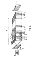
- Fig. 2 shows a schematic of a typical tunable electro-optic filter wherein the low resistivity layers 2 alternate with the high resistivity layers 1 so that the desired voltage V 1 , V 2 , V 3 , etc. can be passed through the low resistivity layers in order to vary the filter transmission characteristic.
- input beam or ray of light from a light source 3 is passed through an input polarizer 4 which establishes a desired linear polarization for the light.
- the light then passes through the tunable birefringent medium (the multi layered structure 5) and an output polarizer or analyzer 6, which passes light polarized along a direction bearing a preselected angular relationship to the direction of polarization of the light emerging from the input polarizer 4.
- an output polarizer or analyzer 6 which passes light polarized along a direction bearing a preselected angular relationship to the direction of polarization of the light emerging from the input polarizer 4.
- Such a device is described in more detail in U.S. Patent 4,197,008.
- the ability to grow layers of AgGaS 2 having defined resistivities ranging from one layer to the next is advantageously employed in fabricating a variety of electro-optical devices, such as tunable filters, modulators, switches, shutters, resonators and the like.
- the silver thiogallate solution from which the epitaxially-grown layers were crystallized was prepared as follows. Nearly 250 grams of high purity silver thiogallate, potassium chloride and germanium were loaded into a quartz crucible. The composition of the mixture was such that the silver thiogallate and germanium combined made up 37.5 mole percent of the mixture and KCI accounted for the other 62.5 mole percent. The mole ratio of germanium to silver thiogallate was 1:4.
- the seed crystal of silver thiogallate used as the substrate upon which the layers were grown was prepared by reacting silver gallium alloys with sulfur vapors. Prior to reaction, the molten silver gallium alloys were equilibrated at 745°C in flowing hydrogen for at least eight hours to provide for reduction of any surface oxides. The reacted silver gallium sulfide polycrystalline compound was then four-pass zone-refined for removal of any small quantities of second phase AggGaS 6 or Ag 2 Ga 1o S 31 precipitates. The Bridgman-Stock- barger method was used to grow a crystal from this material. This bulk crystal was then cut, machined, and prepared for use as a substratel seed crystal.
- the crucible (containing the silver thiogallate, potassium chloride, and germanium) in its quartz growth chamber was evacuated to approximately 10- 4 Pa (10- 6 Torr) at room temperature and then filled with argon to a pressure of about 3.5x 10 4 Pa (five psi).
- the chamber was heated, with crucible enclosed, to a temperature of 880°C and held at this temperature for 12 hours. This permitted the molten solution to equilibrate and reach a homogeneous condition.
- the molten solution was then slowly cooled to 835°C at a rate of 1°C per minute.
- a second layer was then epitaxially grown upon the seed crystal with the germanium-doped layer thereon.
- the second layer did not contain germanium, but was a substantially pure silver thiogallate layer.
- about 250 grams of a 7.5 mol% silver thiogallate and 92.5 mole% potassium mixture was heated to 890°C in a quartz crucible, under an argon atmosphere of about 7x10 3 Pa (1 psi). This molten solution was then maintained as this temperature for 16 hours to allow the ingredients to equilibrate. The solution was then slowly cooled at a rate of 0.5°C/minute to 782°C.
- the seed crystal with the germanium-doped layer thereon was immersed in the molten solution. Subsequently, cooling was commenced at a rate of 0.056°C per minute until the solution temperature reached 773°C. Simultaneously, the seed crystal was rotated at a rate of 5 rpm. On reaching 773°C, the seed crystal with two epitaxially grown layers was withdrawn from the growth solution. The two-layer coated crystal/ substrate was allowed to cool slowly and then was was washed in hot water (80°C) for five minutes. A second layer having a thickness of nearly 18 pm had been grown.
- a third layer approximately 16 pm thick was then epitaxially grown upon the above seeded two-layer structure using the same process described in the first step of this example.
- the multi-step process described in this example permits fabrication of a structure in which different layers exhibit different resistivity.
- the three layer structure produced in this example was a low-resistivity/high-resistivity/ low-resistivity structure wherein the low-resistivity layers exhibited a resistivity of about 6x10 7 ohm-cm and the high-resistivity layer exhibited a resistivity of about 1x10 12 ohm-cm.
- Region III is AgGaS 2 (solid) plus Ge and KCI liquid
- region II above the eutectic is AgGaS 2 (solid) plus Ge (solid) plus KCI liquid. Therefore, in Region III, when a solution is cooled, AgGaS 2 starts to precipitate out as a solid. During this process, the Ge in solution is still liquid and will be dispersed in atomic or molecular form within the liquid solution. In this region, Ge dopant is incorporated in the growing AgGaS 2 epilayer. However, in Region II, both AgGaS 2 and Ge precipitate separately as pure solids. In Region II, AgGaS 2 will grow on the epilayer, but the Ge precipitating out as solid crystallites is excluded by the growing AgGaS 2 epilayer.
- the process in this example requires growth of the low-resistivity Ge-doped layer of AgGaS 2 in Region III and growth of the high-resistivity pure layer of AgGaS 2 in Region II.
- High purity silver thiogallate, potassium chloride and germanium are loaded into a quartz crucible.
- the composition of the mixture is such that the silver thiogallate and germanium combined make up 37.5 mole% of the mixture and potassium chloride accounts for the other 62.5 mole%.
- the mole ratio of germanium to silver thiogallate is 1:4.
- the first layer, doped silver thiogallate, is grown using the procedure and time-temperature conditions described in Example I above.
- the second layer, pure silver thiogallate is grown without the necessity of removing the seed crystal with the germanium-doped layer thereon from the reaction chamber.
- the above structure is simply lifted to the vapor space above the growth solution and the entire chamber is cooled at a rate of about 1 to 2°C per minute until the temperature of the molten solution is within Region II.
- this temperature is about 770°C.
- the seed crystal with the germanium-doped silver thiogallate layer thereon is reimmersed in the molten solution which is then allowed to cool at a rate of 0.05°C per minute.
- a layer of essentially pure silver thiogallate is grown on the germanium-doped layer.
- the seed crystal with the multiple layers of doped and undoped silver thiogallate is removed from the growth solution.
- the thickness of the germanium-doped layer is between 25 and 30 pm, and the thickness of the essentially pure silver thiogallate layer is between 15 and 20 Il m.
- the foregoing process is repeated as many times as needed to form a composite of alternating low and high resistivity layers.
- Example I presents the best mode contemplated for carrying out the multiple growth solutions form of the invention.
- Example II presents a method of carrying out a single growth solution form of the invention.
- the tunable electro-optic filter described above with reference to Fig. 2 is capable of utilizing the multi-layered structure produced by the methods above.
Landscapes
- Chemical & Material Sciences (AREA)
- Engineering & Computer Science (AREA)
- Crystallography & Structural Chemistry (AREA)
- Materials Engineering (AREA)
- Metallurgy (AREA)
- Organic Chemistry (AREA)
- Physics & Mathematics (AREA)
- Nonlinear Science (AREA)
- General Physics & Mathematics (AREA)
- Optics & Photonics (AREA)
- Inorganic Chemistry (AREA)
- Crystals, And After-Treatments Of Crystals (AREA)
Claims (3)
Applications Claiming Priority (2)
| Application Number | Priority Date | Filing Date | Title |
|---|---|---|---|
| US06/605,736 US4589737A (en) | 1984-05-01 | 1984-05-01 | Doped and undoped single crystal multilayered structures |
| US605736 | 1984-05-01 |
Related Child Applications (3)
| Application Number | Title | Priority Date | Filing Date |
|---|---|---|---|
| EP88121028A Division EP0316021A3 (de) | 1984-05-01 | 1985-04-10 | Mehrschichtige Bauelemente aus dotiertem und nicht-dotiertem Einkristall |
| EP88117144.1 Division-Into | 1988-10-14 | ||
| EP88121028.0 Division-Into | 1988-12-15 |
Publications (2)
| Publication Number | Publication Date |
|---|---|
| EP0179852A1 EP0179852A1 (de) | 1986-05-07 |
| EP0179852B1 true EP0179852B1 (de) | 1990-01-24 |
Family
ID=24424998
Family Applications (2)
| Application Number | Title | Priority Date | Filing Date |
|---|---|---|---|
| EP88121028A Withdrawn EP0316021A3 (de) | 1984-05-01 | 1985-04-10 | Mehrschichtige Bauelemente aus dotiertem und nicht-dotiertem Einkristall |
| EP85902246A Expired - Lifetime EP0179852B1 (de) | 1984-05-01 | 1985-04-10 | Dotierte und nicht-dotierte, einkristaline, mehrschichtige strukturen |
Family Applications Before (1)
| Application Number | Title | Priority Date | Filing Date |
|---|---|---|---|
| EP88121028A Withdrawn EP0316021A3 (de) | 1984-05-01 | 1985-04-10 | Mehrschichtige Bauelemente aus dotiertem und nicht-dotiertem Einkristall |
Country Status (7)
| Country | Link |
|---|---|
| US (1) | US4589737A (de) |
| EP (2) | EP0316021A3 (de) |
| JP (1) | JPS61501980A (de) |
| DE (1) | DE3575581D1 (de) |
| DK (1) | DK160325B (de) |
| IL (2) | IL74938A (de) |
| WO (1) | WO1985005134A1 (de) |
Families Citing this family (6)
| Publication number | Priority date | Publication date | Assignee | Title |
|---|---|---|---|---|
| FR2607628B1 (fr) * | 1986-11-27 | 1989-03-17 | Centre Nat Rech Scient | Modulateur optique a superreseau |
| US5212585A (en) * | 1990-04-03 | 1993-05-18 | American Optical Corporation | Laser protective device |
| DE4401626A1 (de) * | 1994-01-20 | 1995-07-27 | Max Planck Gesellschaft | Verfahren und Vorrichtung zur Herstellung kristalliner Schichten |
| US6795605B1 (en) * | 2000-08-01 | 2004-09-21 | Cheetah Omni, Llc | Micromechanical optical switch |
| US7145704B1 (en) | 2003-11-25 | 2006-12-05 | Cheetah Omni, Llc | Optical logic gate based optical router |
| US6888661B1 (en) | 2002-06-13 | 2005-05-03 | Cheetah Omni, Llc | Square filter function tunable optical devices |
Family Cites Families (12)
| Publication number | Priority date | Publication date | Assignee | Title |
|---|---|---|---|---|
| US3345141A (en) * | 1963-11-07 | 1967-10-03 | Perkin Elmer Corp | Growth of calcite crystals from a molten flux by slow cooling |
| US4001076A (en) * | 1974-12-11 | 1977-01-04 | Gte Laboratories Incorporated | Method for growing thin epitaxial layers of a non-linear, optically active material |
| JPS5228867A (en) * | 1975-08-29 | 1977-03-04 | Sanyo Electric Co Ltd | Process for formation of pn junction |
| JPS5437098A (en) * | 1977-08-30 | 1979-03-19 | Toshiba Corp | Method of producing gallium phosphide greenish luminous element |
| US4197008A (en) | 1977-12-27 | 1980-04-08 | Hughes Aircraft Company | Electro-optic tunable optical filter |
| US4229073A (en) * | 1979-08-10 | 1980-10-21 | Hughes Aircraft Company | Iso-index coupled-wave electro-optic filters |
| US4247166A (en) * | 1979-08-15 | 1981-01-27 | Rockwell International Corporation | Single plate birefringent optical filter |
| US4240696A (en) | 1979-11-13 | 1980-12-23 | Rockwell International Corporation | Multilayer electro-optically tunable filter |
| US4350413A (en) | 1980-04-14 | 1982-09-21 | The United States Of America As Represented By The Secretary Of The Navy | Multi-color tunable filter |
| US4500178A (en) * | 1981-10-13 | 1985-02-19 | Rockwell International Corporation | Iso-index birefringent filters |
| US4540461A (en) | 1984-04-30 | 1985-09-10 | Hughes Aircraft Company | Silver thiogallate single crystal layers epitaxially grown from potassium chloride-silver thiogallate solution |
| US4534822A (en) | 1984-04-30 | 1985-08-13 | Hughes Aircraft Company | Method of synthesizing thin, single crystal layers of silver thiogallate (AgGaS2) |
-
1984
- 1984-04-16 IL IL74938A patent/IL74938A/xx unknown
- 1984-05-01 US US06/605,736 patent/US4589737A/en not_active Expired - Fee Related
-
1985
- 1985-04-10 EP EP88121028A patent/EP0316021A3/de not_active Withdrawn
- 1985-04-10 WO PCT/US1985/000623 patent/WO1985005134A1/en not_active Ceased
- 1985-04-10 DE DE8585902246T patent/DE3575581D1/de not_active Expired - Fee Related
- 1985-04-10 EP EP85902246A patent/EP0179852B1/de not_active Expired - Lifetime
- 1985-04-10 JP JP60501861A patent/JPS61501980A/ja active Granted
- 1985-04-16 IL IL74938A patent/IL74938A0/xx unknown
- 1985-12-30 DK DK609585A patent/DK160325B/da not_active Application Discontinuation
Also Published As
| Publication number | Publication date |
|---|---|
| IL74938A (en) | 1988-12-30 |
| IL74938A0 (en) | 1985-08-30 |
| JPS61501980A (ja) | 1986-09-11 |
| DK609585A (da) | 1986-01-14 |
| EP0316021A2 (de) | 1989-05-17 |
| WO1985005134A1 (en) | 1985-11-21 |
| EP0316021A3 (de) | 1989-12-13 |
| EP0179852A1 (de) | 1986-05-07 |
| DK609585D0 (da) | 1985-12-30 |
| JPH0542400B2 (de) | 1993-06-28 |
| US4589737A (en) | 1986-05-20 |
| DE3575581D1 (de) | 1990-03-01 |
| DK160325B (da) | 1991-02-25 |
Similar Documents
| Publication | Publication Date | Title |
|---|---|---|
| EP0600658A2 (de) | Pufferschicht aus epitaktischen Magnesiumoxid auf Tetrahedrischen Halbleitern | |
| JPH06244407A (ja) | (111)方位緩衝層を有する多層構造体 | |
| EP0444209B1 (de) | Dünnfilmeinzelkristall aus lithiumniobat und verfahren zu seiner herstellung | |
| EP0179852B1 (de) | Dotierte und nicht-dotierte, einkristaline, mehrschichtige strukturen | |
| Kawaguchi et al. | Growth of high crystalline quality LiNbO3 thin films by a new liquid phase epitaxial technique from a solid-liquid coexisting melt | |
| EP0413159A2 (de) | Verfahren zum Aufwachsen von zusammengesetzten Halbleiterschichten und Detektor aufgebaut aus solchen | |
| EP0547061B1 (de) | DURCH EPITAXIE AUS DER FLÜSSIGPHASE HERGESTELLTE M1-xNxTiAs1-aPa05 WELLENLEITER | |
| EP0311038B1 (de) | Verfahren zum Erzeugen von monokristallinen Quecksilber-Cadmium-Tellurid-Schichten | |
| US4534822A (en) | Method of synthesizing thin, single crystal layers of silver thiogallate (AgGaS2) | |
| CA1149709A (en) | Magneto-optic bi.sub.1 lu.sub.2 fe.sub.5 o in12 xx crystals | |
| JP3479111B2 (ja) | 電気光学品 | |
| RU2699639C1 (ru) | Нелинейный монокристалл литиевых халькогенидов общей формулы LiGaxIn1-xTe2 и способ его получения | |
| EP0690152B1 (de) | Verfahren und Vorrichtung zur Herstellung einkristalliner Oxydfilmen | |
| Sashital et al. | A multilayer AgGaS2 structure for infrared (2–10 μm) electro‐optic tunable filters: Fabrication and performance | |
| US5077239A (en) | Chalcogenide glass, associated method and apparatus | |
| Akishige | Temperature dependence of the optical absorption edge in hexagonal BaTiO3 | |
| JPH07311370A (ja) | 電気光学品及びその製造方法 | |
| US3914525A (en) | Mercury sulfide films and method of growth | |
| Azoulay et al. | The growth of a cubic, single phase, Cd0. 6Mn0. 4Te single crystal by the vertical gradient freeze method | |
| JP3348129B2 (ja) | 電気光学品の製造方法 | |
| JPH11322497A (ja) | ニオブ酸リチウム単結晶膜およびその製造方法 | |
| Feigelson | Heavy Metal Ternary Compounds for Infrared Acousto-Optic Applications | |
| JPH07234427A (ja) | 非線型光学材料の製造方法 | |
| JP3030584B2 (ja) | 化合物半導体単結晶の製造方法および製造装置 | |
| Pandey et al. | Synthesis and dielectric characterization of Pb-K-niobate SAW-single crystal |
Legal Events
| Date | Code | Title | Description |
|---|---|---|---|
| PUAI | Public reference made under article 153(3) epc to a published international application that has entered the european phase |
Free format text: ORIGINAL CODE: 0009012 |
|
| 17P | Request for examination filed |
Effective date: 19851115 |
|
| AK | Designated contracting states |
Kind code of ref document: A1 Designated state(s): CH DE FR IT LI NL SE |
|
| RAP1 | Party data changed (applicant data changed or rights of an application transferred) |
Owner name: HUGHES AIRCRAFT COMPANY |
|
| 17Q | First examination report despatched |
Effective date: 19870608 |
|
| R17C | First examination report despatched (corrected) |
Effective date: 19870612 |
|
| GRAA | (expected) grant |
Free format text: ORIGINAL CODE: 0009210 |
|
| AK | Designated contracting states |
Kind code of ref document: B1 Designated state(s): CH DE FR IT LI NL SE |
|
| XX | Miscellaneous (additional remarks) |
Free format text: TEILANMELDUNG 88117144.1 EINGEREICHT AM 10/04/85. |
|
| REF | Corresponds to: |
Ref document number: 3575581 Country of ref document: DE Date of ref document: 19900301 |
|
| ET | Fr: translation filed | ||
| PGFP | Annual fee paid to national office [announced via postgrant information from national office to epo] |
Ref country code: FR Payment date: 19900310 Year of fee payment: 6 |
|
| PGFP | Annual fee paid to national office [announced via postgrant information from national office to epo] |
Ref country code: SE Payment date: 19900319 Year of fee payment: 6 |
|
| PGFP | Annual fee paid to national office [announced via postgrant information from national office to epo] |
Ref country code: CH Payment date: 19900321 Year of fee payment: 6 |
|
| ITF | It: translation for a ep patent filed | ||
| PGFP | Annual fee paid to national office [announced via postgrant information from national office to epo] |
Ref country code: DE Payment date: 19900330 Year of fee payment: 6 |
|
| ITTA | It: last paid annual fee | ||
| PGFP | Annual fee paid to national office [announced via postgrant information from national office to epo] |
Ref country code: NL Payment date: 19900430 Year of fee payment: 6 |
|
| PLBE | No opposition filed within time limit |
Free format text: ORIGINAL CODE: 0009261 |
|
| STAA | Information on the status of an ep patent application or granted ep patent |
Free format text: STATUS: NO OPPOSITION FILED WITHIN TIME LIMIT |
|
| 26N | No opposition filed | ||
| PG25 | Lapsed in a contracting state [announced via postgrant information from national office to epo] |
Ref country code: SE Effective date: 19910411 |
|
| PG25 | Lapsed in a contracting state [announced via postgrant information from national office to epo] |
Ref country code: LI Effective date: 19910430 Ref country code: CH Effective date: 19910430 |
|
| PG25 | Lapsed in a contracting state [announced via postgrant information from national office to epo] |
Ref country code: NL Effective date: 19911101 |
|
| NLV4 | Nl: lapsed or anulled due to non-payment of the annual fee | ||
| PG25 | Lapsed in a contracting state [announced via postgrant information from national office to epo] |
Ref country code: FR Effective date: 19911230 |
|
| REG | Reference to a national code |
Ref country code: CH Ref legal event code: PL |
|
| PG25 | Lapsed in a contracting state [announced via postgrant information from national office to epo] |
Ref country code: DE Effective date: 19920201 |
|
| REG | Reference to a national code |
Ref country code: FR Ref legal event code: ST |
|
| EUG | Se: european patent has lapsed |
Ref document number: 85902246.9 Effective date: 19911108 |