EP0178043A1 - Netzteil für eine Elektrolumineszenzanzeige - Google Patents
Netzteil für eine Elektrolumineszenzanzeige Download PDFInfo
- Publication number
- EP0178043A1 EP0178043A1 EP85305276A EP85305276A EP0178043A1 EP 0178043 A1 EP0178043 A1 EP 0178043A1 EP 85305276 A EP85305276 A EP 85305276A EP 85305276 A EP85305276 A EP 85305276A EP 0178043 A1 EP0178043 A1 EP 0178043A1
- Authority
- EP
- European Patent Office
- Prior art keywords
- circuit
- voltage
- panel
- power supply
- power
- Prior art date
- Legal status (The legal status is an assumption and is not a legal conclusion. Google has not performed a legal analysis and makes no representation as to the accuracy of the status listed.)
- Granted
Links
- 230000010355 oscillation Effects 0.000 claims abstract description 16
- 238000004804 winding Methods 0.000 claims description 24
- 239000003112 inhibitor Substances 0.000 claims description 5
- 230000004907 flux Effects 0.000 claims description 2
- 239000003990 capacitor Substances 0.000 description 5
- 238000010586 diagram Methods 0.000 description 3
- 238000010276 construction Methods 0.000 description 2
- 230000000694 effects Effects 0.000 description 2
- 230000002401 inhibitory effect Effects 0.000 description 2
- 230000000903 blocking effect Effects 0.000 description 1
- 230000008878 coupling Effects 0.000 description 1
- 238000010168 coupling process Methods 0.000 description 1
- 238000005859 coupling reaction Methods 0.000 description 1
- 230000007423 decrease Effects 0.000 description 1
- 230000000994 depressogenic effect Effects 0.000 description 1
- 238000010438 heat treatment Methods 0.000 description 1
- 235000003642 hunger Nutrition 0.000 description 1
- 238000005286 illumination Methods 0.000 description 1
- 238000003780 insertion Methods 0.000 description 1
- 230000037431 insertion Effects 0.000 description 1
- 230000007257 malfunction Effects 0.000 description 1
- 239000000463 material Substances 0.000 description 1
- 239000004065 semiconductor Substances 0.000 description 1
- 239000007787 solid Substances 0.000 description 1
- 230000037351 starvation Effects 0.000 description 1
Images


Classifications
-
- H—ELECTRICITY
- H02—GENERATION; CONVERSION OR DISTRIBUTION OF ELECTRIC POWER
- H02H—EMERGENCY PROTECTIVE CIRCUIT ARRANGEMENTS
- H02H7/00—Emergency protective circuit arrangements specially adapted for specific types of electric machines or apparatus or for sectionalised protection of cable or line systems, and effecting automatic switching in the event of an undesired change from normal working conditions
- H02H7/10—Emergency protective circuit arrangements specially adapted for specific types of electric machines or apparatus or for sectionalised protection of cable or line systems, and effecting automatic switching in the event of an undesired change from normal working conditions for converters; for rectifiers
- H02H7/12—Emergency protective circuit arrangements specially adapted for specific types of electric machines or apparatus or for sectionalised protection of cable or line systems, and effecting automatic switching in the event of an undesired change from normal working conditions for converters; for rectifiers for static converters or rectifiers
- H02H7/122—Emergency protective circuit arrangements specially adapted for specific types of electric machines or apparatus or for sectionalised protection of cable or line systems, and effecting automatic switching in the event of an undesired change from normal working conditions for converters; for rectifiers for static converters or rectifiers for inverters, i.e. DC/AC converters
- H02H7/1227—Emergency protective circuit arrangements specially adapted for specific types of electric machines or apparatus or for sectionalised protection of cable or line systems, and effecting automatic switching in the event of an undesired change from normal working conditions for converters; for rectifiers for static converters or rectifiers for inverters, i.e. DC/AC converters responsive to abnormalities in the output circuit, e.g. short circuit
-
- H—ELECTRICITY
- H05—ELECTRIC TECHNIQUES NOT OTHERWISE PROVIDED FOR
- H05B—ELECTRIC HEATING; ELECTRIC LIGHT SOURCES NOT OTHERWISE PROVIDED FOR; CIRCUIT ARRANGEMENTS FOR ELECTRIC LIGHT SOURCES, IN GENERAL
- H05B44/00—Circuit arrangements for operating electroluminescent light sources
-
- H—ELECTRICITY
- H05—ELECTRIC TECHNIQUES NOT OTHERWISE PROVIDED FOR
- H05B—ELECTRIC HEATING; ELECTRIC LIGHT SOURCES NOT OTHERWISE PROVIDED FOR; CIRCUIT ARRANGEMENTS FOR ELECTRIC LIGHT SOURCES, IN GENERAL
- H05B41/00—Circuit arrangements or apparatus for igniting or operating discharge lamps
- H05B41/14—Circuit arrangements
- H05B41/36—Controlling
- H05B41/38—Controlling the intensity of light
- H05B41/39—Controlling the intensity of light continuously
- H05B41/392—Controlling the intensity of light continuously using semiconductor devices, e.g. thyristor
-
- Y—GENERAL TAGGING OF NEW TECHNOLOGICAL DEVELOPMENTS; GENERAL TAGGING OF CROSS-SECTIONAL TECHNOLOGIES SPANNING OVER SEVERAL SECTIONS OF THE IPC; TECHNICAL SUBJECTS COVERED BY FORMER USPC CROSS-REFERENCE ART COLLECTIONS [XRACs] AND DIGESTS
- Y02—TECHNOLOGIES OR APPLICATIONS FOR MITIGATION OR ADAPTATION AGAINST CLIMATE CHANGE
- Y02B—CLIMATE CHANGE MITIGATION TECHNOLOGIES RELATED TO BUILDINGS, e.g. HOUSING, HOUSE APPLIANCES OR RELATED END-USER APPLICATIONS
- Y02B20/00—Energy efficient lighting technologies, e.g. halogen lamps or gas discharge lamps
- Y02B20/30—Semiconductor lamps, e.g. solid state lamps [SSL] light emitting diodes [LED] or organic LED [OLED]
Definitions
- This invention relates to power supplies for electroluminescent (EL) panels, and more particularly to power supplies which effectively are inhibited or blocked and thus shut down in the event of a short in the panel circuit or a panel failure.
- the application is further directed to particular power supplies for such panels including a transformerless power supply.
- electroluminescent panels particularly in the automotive and aircraft field, has required the development of DC operated power supplies for such panels, which can conveniently take a low voltage source of DC power available, and provide an operating voltage for the electroluminescent panels involved.
- EL panels have come into widespread use in light aircraft having only a DC power system, for enunciator panels or for other illumination devices, and in automobiles as a design feature such as for opera lights, or for backlighting of radio controls or the like.
- a need for low cost, lightweight and dependable power supplies which can operate on a low voltage direct current source, such as 12 volts DC, and provide dependenable power for the electroluminescent lamp or panel.
- a further requirement has been that of providing a power supply which is blocked or inhibited and is thus failsafe on the occurrence of an electrical or mechanical malfunction in the panel itself, causing the panel to short.
- Shorting of the FL panel may result by reason of improper construction of the panel itself or mechanical abuse or catastrophic failures.
- such shorting has tended to place an uncommonly high load upon the inverter power supply, to the point where the power supply may fail, and in failing, may cause an electrical hazard, such as an overload, or a source of localized heating, which can under certain circumstances cause a fire hazard.
- an electric drive circuit for an electroluminescent panel or the like operating from a low voltage source of DC power, including an oscillator circuit connected to said low voltage source, and a voltage step-up device connected to the oscillator circuit for driving the electroluminescent panel, is characterised by an inhibitor circuit responsive to a short circuit of said panel for preventing further oscillation of the oscillator circuit and reducing the power drawn from the power supply to a lower safe value.
- the power supply consists of an inverter circuit incorporating an autotransformer, with the electroluminescent panel forming a capacitive load on the transformer winding, with the circuit being arranged such that shorting of the panel results in a reflected low impedance to appear across the normally high collector impedance circuit to the point that oscillations are no longer possible.
- the current normally drawn by the circuit dropping to a minimum value.
- a power supply which is transformerless and which employs a voltage multiplying circuit driving a self-sustaining output circuit, which output circuit is inhibited in such a manner that shorting of the panel results in a starvation of the power supply to the output circuit, and a cessation of operation of the oscillator, with the result that little or no current flows.
- Each of the embodiments is characterized by the fact that shorting of the EL panel results in the load on the DC power source dropping to a minimum, in a fail-safe condition.
- an electronic drive circuit for an electroluminescent panel operates from a low voltage source of DC power and includes an oscillator circuit which is connected to the low voltage source and further includes a voltage step-up device such as a transformer or a voltage multiplier circuit which is connected to the oscillator circuit and which drive the electroluminescent panel characterized by an inhibitor circuit, which may include the feedback winding of the autotransformer and a current limiting resistor or which may include an emitter-follower and voltage divider, which prevent further osciallations of the oscillator circuit and reduce the power drawn from the D C power supply to a lower safe value in the event of failure, such as shorting, of the electroluminescent panel.
- a self-inhibiting power supply for an EL lamp is shown in Fig. 1.
- the electroluminescent lamp or panel is illustrated generally by the capacitance 10 and is shown as being connected to top A of winding N3 of an autotransformer 12.
- the power source or input to the power supply may be a 12 volt battery or the like, and is designated by the reference numeral 14.
- the transformer 12, in addition to the winding N3, includes windings N1 and N2 defined by taps B, C and D, with a common grounded tap C. Winding N1 is in the collector circuit of a PNP drive transistor 20, while winding N2 is coupled to the base circuit through capacitor 21. Power is applied to and through a series connected diode 22 and resistor 24, and the emitter of transistor 20.
- a second diode 25 is connected from the base to the junction of the diode 22 and the resistor 24, and permits the positive half of the feedback cycle to be returned to the emitter.
- a capacitor 26 may be connected from terminal D to ground, to prevent spurious oscillations and to tune the primary winding Nl.
- windings of the transformer 12 are and remain essentially at DC ground potential since tap C is grounded.
- the resistor 2R in the feedback circuit from terminal B to the base is selected so as to start the circuit oscillations, and limit the direct current drawn when the output terminal A is at zero DC potential, in the event that the electroluminescent panel 10 for any reason becomes grounded or shorted.
- the frequency of oscillations depends upon the maximum flux density, which in turn depends upon the ampere turns of the primary winding N1 and the reflected capacitance of EL panel 10 into the primary.
- the voltage fed to the base of the transistor 20 is in phase with the collector voltage, and starts and maintains oscillations in normal operation.
- the feedback winding N2 has in the order of half the turns of the primary winding N1, and the diode 25 is connected in such a manner as to to allow the positive half of the feedback cycle to return to the emitter of the transistor 20.
- the negative half cycle is rectified by the base emitter junction of the transistor, which in turn causes the transistor to pass more current from the emitter to the collector. During operation, under no load condition, the transistor draws nearly its maximum current.
- the power supply When a load, such as the EL panel 10, is applied between the output terminal A and ground, which uses less energy than the energy being fed to the base emitter junction, the power supply continues to operate. However, in the event that the panel 10 becomes shorted or otherwise dissipates excessive energy, the oscillator circuit is substantia-lly detuned and insufficient energy is fed through capacitor 21 into the base to establish or maintain oscillations. In effect, the oscillator becomes "starved" for current and the current which the transistor 20 now passes will be determined by the value of resistance 28,-which provides a small forward bias current, which in turn causes a very low collector current.
- the resistor 24 is a resistor of small value, to limit the maximum current which the power supply can drawn from the main power source 14. Accordingly, in the event that a short circuit occurs in the EL panel 10 or the leads to the panel, or even in the transformer 12, the power supply shown in Fig. 1 virtually shuts down and idles at very low current input compared to the normal operating input current.
- a single transistor power supply has been made in accordance with the teachings of the invention as shown in Fig. 1 and draws 300-350 milliamps from a 12.6 volt power source under full load.
- the output was 20 milliamps at 140 V, 200 Hertz.
- the DC current that is drawn goes to a very low level in the order of 10-12 milliamperes.
- the resistor 28 in the base circuit of the transistor 20 in combination with the current limiting resistor 24, may be considered as current limiting means for inhibiting or blocking oscillations in the event that the transformer secondary winding N3 or the EL panel 10, or the lead to the panel becomes shorted or otherwise becomes grounded, thereby automatically shutting down the power supply.
- the following table is a list of circuit elements which have actually been used in the example of the invention as described above in ccnnec- tion with Fig. 1 of the application:
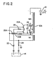
- Fig. 2 shows a push/pull version of the current limiting circuit of this invention, according to the embodiment of Fig. 1 employing the principles used in the single transistor power supply of Fig. 1.
- parts in the embodiment of Fig. 2 which correspond more or less directly to the same parts used in the embodiment of Fig. 1 have been identified with like reference numerals.
- a pair of PNP drive transistors 20a and 20b are connected in push/pull relation with their emitters connected in common through the current limiting resistor 28.
- the transformer 12a differs from the transformer 12 in that the feedback winding N1 is isolated from the secondary winding which now includes push/pull windings N2 and N3, center tapped, and connected respectively to the collectors of the transistors 20a and 20b.
- the secondary winding N4 is connected to the EL lamp or panel 10.
- the terminals of the feedback winding N1 of the embodiment of Fig. 2 are connected to the respective bases of the transistors 20a and 20b.
- the starting resistor 24 i ⁇ connected to the bases of the transistors, while the semi-conductor diodes 25a and 25b provide a return path for the positive going potential appearing at each of the respective bases on the alternate half-cycle portions of the feedback potential.
- the purpose of the resistor 24 is to limit current which the circuit can draw in the event of a short.
- a unique feature of the circuit of Fig. 2 is the fact that the feedback winding Nl is not center tapped, thus reducing the cost. Further, like the power supply circuit of Fig. 1, the secondary winding of the transformer 12a is maintained essentially at a DC ground potential.
- a further embodiment is in the form of a transformerless, short circuit protected EL lamp power supply, as shown in Fig. 3.
- the circuit of Fig. 3 utilizes a high frequency oscillator which supplies power to a voltage muliplier circuit which, in turn, supplies high voltage to the driver transistors for the panel.
- a relatively lower frequency oscillator controls the application of the high voltage provided by the voltage multiplier at a substantially lower frequency for the purpose of maintaining the longevity of the panel.
- a CMOS circuit 49 includes NAND gates A, B, C, and D.
- NAND gates A and B constitute a high frequency oscillator having a frequency in the order of approximately 20 kilohertz, for example.
- the outputs of the oscillator defined by the gates A and B appears on lines 50 and 51 in the form of a push/pull square wave, which wave is fed through coupling capacitors C13 and C14 to the bases of output driver pairs Q1-Q3 and Q2-Q4.
- the output driver pairs receive their power direct from the DC voltage source 14 through a common line 55, and the output thereof designated as Vm is applied to the input of a voltage multipler 60.
- the voltage multiplier 60 consists of diodes CR1 thorugh CR5 and capacitors C3 through C12, arranged in a voltage multiplier ladder.
- the output square wave potential V applied to the power amplifiers Q1-Q4 and applied by these amplifiers to the input of the voltage multiplier, is very nearly the same as the applied DC.potential by the source 14, which may be 12.6 volts, for example.
- the output of the voltage multiplier 60 appears on line 62 and may be, for example, in the order of 140 volts and is fed to a voltage divider consisting of resistors R7 and R8. It is also fed to the input of EL lamp totem pole drivers Q5 through Q8.
- drivers Q5 and Q6 are arranged in totem pole driving fashion as are drivers Q7 and Q8, with the respective input terminals of the EL lamp 10 connected across the emitters of drivers Q5 and Q7.
- the multiplied voltage on line 62 is applied to the collectors of Q5 and Q7 for powering the lamp 10.
- the totem pole pairs Q5-Q6 and Q7-Q8 are arranged in push/pull and are controlled by a relatively lower frequency oscillator consisting of NAND gates C and D, within the same integrated circuit 49.
- the oscillator defined by the NAND gates C and D is designed to operate at a substantially lower frequency which may be in the order of 1000 Hertz, to maintain the longevity of the EL panel.
- the output of the low frequency oscillator is a square wave applied by lines 65 and 66 through resistors R3 and R4 to the respective bases of control devices Q6 and Q8.
- Means for starting and maintaining oscillations includes a momentary starting switch 70, which, when depressed, applies input DC power from line 55 to a line 72 connected to the in p out of the CMOS circuit 49.
- the base of an emitter follower Q9 is connected to the junction of the voltage divider resistors R7 and R8, and when conducting, continues to apply CMOS oscillator operating power to the line 72.
- the emitter follower Q9 derives its collector DC power from the external power source 14 on line 55. Oscillations then begin in the oscillators which energizes the DC voltage multiplier 60, which now feeds the emitter follower Q9 which in turn maintains a DC power source for the CMOS integrated circuit.
- the momentary switch 70 is released, the oscillations will continue unless and until the output of the voltage multiplier is overloaded for whatever reason, usually associated with failure of the EL lamp, as previously defined.
- the load which is imposed through the drivers Q5 and Q7 to the voltage multiplier circuit 60 immediately and substantially reduces the output voltage.
- the reduction of the output voltage on line 62 correspondingly reduces the voltage at the base of the emitter follower Q9, which causes the emitter follower to cut ofi which in turn cuts the system off completely.
- the emitter follower Q9 and the voltage divider R7 and R8 provides means defining an inhibitor circuit which is operable, with failure or excessive load reflected at the panel 10, to shut down the power supply for the EL and thus prevent either catastrophic loss or darage to the power supply or to the surrounding equipment cr material.
- this anpli- cation provides both transformer and transformerless safety oriented electronic power supplies for driving EL lamps, and which protect themselves as well as their associated circuitry against excessive current loads in the event of a problem or failure at the EL lamp.
- the hybrid circuit shown in Fig. 3 has the particular advantage of compactness, and since no transformer is needed, the entire circuit of Fig. 3 may conveniently be fabricated directly to an EL lamp itself or to a small circuit board or chip associated with the EL lamp.
Landscapes
- Engineering & Computer Science (AREA)
- Power Engineering (AREA)
- Physics & Mathematics (AREA)
- Microelectronics & Electronic Packaging (AREA)
- Optics & Photonics (AREA)
- Electroluminescent Light Sources (AREA)
- Dc-Dc Converters (AREA)
- Protection Of Static Devices (AREA)
Applications Claiming Priority (2)
| Application Number | Priority Date | Filing Date | Title |
|---|---|---|---|
| US635770 | 1984-07-30 | ||
| US06/635,770 US4595861A (en) | 1984-07-30 | 1984-07-30 | Power supplies for electroluminescent panels |
Related Child Applications (1)
| Application Number | Title | Priority Date | Filing Date |
|---|---|---|---|
| EP88112557.9 Division-Into | 1985-07-24 |
Publications (2)
| Publication Number | Publication Date |
|---|---|
| EP0178043A1 true EP0178043A1 (de) | 1986-04-16 |
| EP0178043B1 EP0178043B1 (de) | 1990-05-23 |
Family
ID=24549054
Family Applications (2)
| Application Number | Title | Priority Date | Filing Date |
|---|---|---|---|
| EP88112557A Withdrawn EP0308634A1 (de) | 1984-07-30 | 1985-07-24 | Netzteil für Elektrolumineszenzpanele |
| EP85305276A Expired - Lifetime EP0178043B1 (de) | 1984-07-30 | 1985-07-24 | Netzteil für eine Elektrolumineszenzanzeige |
Family Applications Before (1)
| Application Number | Title | Priority Date | Filing Date |
|---|---|---|---|
| EP88112557A Withdrawn EP0308634A1 (de) | 1984-07-30 | 1985-07-24 | Netzteil für Elektrolumineszenzpanele |
Country Status (6)
| Country | Link |
|---|---|
| US (1) | US4595861A (de) |
| EP (2) | EP0308634A1 (de) |
| JP (1) | JPS6188491A (de) |
| BR (1) | BR8503588A (de) |
| CA (1) | CA1237837A (de) |
| DE (1) | DE3577951D1 (de) |
Cited By (1)
| Publication number | Priority date | Publication date | Assignee | Title |
|---|---|---|---|---|
| WO2008140663A2 (en) | 2007-05-09 | 2008-11-20 | Nordson Corporation | Nozzle with internal filter |
Families Citing this family (14)
| Publication number | Priority date | Publication date | Assignee | Title |
|---|---|---|---|---|
| US4697930A (en) * | 1986-07-03 | 1987-10-06 | Spartus Corporation | Transformerless clock circuit with duplex optoelectronic display |
| US4769753A (en) * | 1987-07-02 | 1988-09-06 | Minnesota Mining And Manufacturing Company | Compensated exponential voltage multiplier for electroluminescent displays |
| JPH02143297A (ja) * | 1988-11-25 | 1990-06-01 | Alps Electric Co Ltd | El表示素子の駆動回路 |
| US4954752A (en) * | 1988-12-09 | 1990-09-04 | United Technologies Corporation | Row driver for EL panels and the like with transformer coupling |
| US4982314A (en) * | 1988-12-09 | 1991-01-01 | Nichia Kagaku Kogyo K.K. | Power source circuit apparatus for electro-luminescence device |
| US5089748A (en) * | 1990-06-13 | 1992-02-18 | Delco Electronics Corporation | Photo-feedback drive system |
| US5359341A (en) * | 1992-04-22 | 1994-10-25 | Tek Electronics Manufacturing Corporation | Power supply for sequentially energizing segments of an electroluminescent panel to produce animated displays |
| JPH06334119A (ja) * | 1993-02-17 | 1994-12-02 | Seiko Instr Inc | 昇圧用半導体集積回路及びその半導体集積回路を用いた電子機器 |
| EP0661749A1 (de) * | 1993-12-28 | 1995-07-05 | Seiko Instruments Inc. | Integrierte Halbleiterschaltung für einen Spannungshöher und elektronische Anordnung für eine solche integrierte Halbleiterschaltung |
| US5463283A (en) * | 1994-05-24 | 1995-10-31 | Bkl, Inc. | Drive circuit for electroluminescent lamp |
| AUPO721597A0 (en) * | 1997-06-05 | 1997-07-03 | Lumitex Pty Ltd | An apparatus for driving an electro-luminescent device |
| JP4260226B2 (ja) * | 1997-08-01 | 2009-04-30 | コーニンクレッカ フィリップス エレクトロニクス エヌ ヴィ | 回路装置及びこの回路装置を具備する信号灯 |
| US6043610A (en) * | 1998-07-16 | 2000-03-28 | Durel Corporation | Battery operated power supply including a low level boost and a high level boost |
| TW200503585A (en) * | 2003-07-07 | 2005-01-16 | Primax Electronics Ltd | Lamp inverter |
Citations (4)
| Publication number | Priority date | Publication date | Assignee | Title |
|---|---|---|---|---|
| GB1469035A (en) * | 1974-02-15 | 1977-03-30 | Ncr Co | Voltage converting apparatus |
| FR2398427A1 (fr) * | 1977-07-19 | 1979-02-16 | Legrand Sa | Dispositif d'alimentation pour tubes fluorescents, et application notamment aux blocs d'eclairage de securite |
| EP0058035A1 (de) * | 1981-02-04 | 1982-08-18 | Toshiba Electric Equipment Corporation | Transistor-Inverterschaltung |
| GB2113937A (en) * | 1982-01-21 | 1983-08-10 | Sonca Ind Ltd | Improvements relating to inverter circuits |
Family Cites Families (12)
| Publication number | Priority date | Publication date | Assignee | Title |
|---|---|---|---|---|
| JPS453116Y1 (de) * | 1967-02-16 | 1970-02-10 | ||
| JPS5124982A (en) * | 1974-08-24 | 1976-02-28 | Tdk Electronics Co Ltd | Dengensochino anteikakairo |
| US4028596A (en) * | 1974-12-13 | 1977-06-07 | Coulter Information Systems, Inc. | Corona power supply circuit |
| US4004188A (en) * | 1975-09-26 | 1977-01-18 | General Electric Company | Starting circuit for inverter operated gaseous discharge lamps |
| IT1067179B (it) * | 1976-07-07 | 1985-03-12 | Sits Soc It Telecom Siemens | Fusibile elettronico |
| JPS545532A (en) * | 1977-06-15 | 1979-01-17 | Nippon Telegr & Teleph Corp <Ntt> | Stop system for inverter |
| US4319164A (en) * | 1979-07-30 | 1982-03-09 | Midland-Ross Corporation | Power factor compensating electroluminescent lamp DC/AC inverter |
| EP0027015B1 (de) * | 1979-10-04 | 1984-06-27 | Imperial Chemical Industries Plc | Gleichstrom-Gleichstrom-Umformer |
| JPS5856111A (ja) * | 1981-09-30 | 1983-04-02 | Toshiba Electric Equip Corp | 電源装置 |
| JPS5863083A (ja) * | 1981-10-09 | 1983-04-14 | Murata Mfg Co Ltd | 自励発振型高圧電源 |
| US4453193A (en) * | 1982-10-12 | 1984-06-05 | General Electric Company | Overcurrent protection for push-pull circuits |
| US4498128A (en) * | 1983-07-07 | 1985-02-05 | At&T Bell Laboratories | Current limit circuit in single-ended forward converter utilizing core reset to initiate power switch conduction |
-
1984
- 1984-07-30 US US06/635,770 patent/US4595861A/en not_active Expired - Fee Related
-
1985
- 1985-07-24 DE DE8585305276T patent/DE3577951D1/de not_active Expired - Fee Related
- 1985-07-24 EP EP88112557A patent/EP0308634A1/de not_active Withdrawn
- 1985-07-24 EP EP85305276A patent/EP0178043B1/de not_active Expired - Lifetime
- 1985-07-29 CA CA000487719A patent/CA1237837A/en not_active Expired
- 1985-07-29 BR BR8503588A patent/BR8503588A/pt not_active IP Right Cessation
- 1985-07-30 JP JP60166959A patent/JPS6188491A/ja active Pending
Patent Citations (4)
| Publication number | Priority date | Publication date | Assignee | Title |
|---|---|---|---|---|
| GB1469035A (en) * | 1974-02-15 | 1977-03-30 | Ncr Co | Voltage converting apparatus |
| FR2398427A1 (fr) * | 1977-07-19 | 1979-02-16 | Legrand Sa | Dispositif d'alimentation pour tubes fluorescents, et application notamment aux blocs d'eclairage de securite |
| EP0058035A1 (de) * | 1981-02-04 | 1982-08-18 | Toshiba Electric Equipment Corporation | Transistor-Inverterschaltung |
| GB2113937A (en) * | 1982-01-21 | 1983-08-10 | Sonca Ind Ltd | Improvements relating to inverter circuits |
Cited By (1)
| Publication number | Priority date | Publication date | Assignee | Title |
|---|---|---|---|---|
| WO2008140663A2 (en) | 2007-05-09 | 2008-11-20 | Nordson Corporation | Nozzle with internal filter |
Also Published As
| Publication number | Publication date |
|---|---|
| US4595861A (en) | 1986-06-17 |
| EP0308634A1 (de) | 1989-03-29 |
| DE3577951D1 (de) | 1990-06-28 |
| EP0178043B1 (de) | 1990-05-23 |
| CA1237837A (en) | 1988-06-07 |
| BR8503588A (pt) | 1986-04-29 |
| JPS6188491A (ja) | 1986-05-06 |
Similar Documents
| Publication | Publication Date | Title |
|---|---|---|
| EP0178043A1 (de) | Netzteil für eine Elektrolumineszenzanzeige | |
| US4801887A (en) | Circuit arrangement for generating a direct voltage from a sinusoidal input voltage | |
| US4970620A (en) | FET bridge protection circuit | |
| US5811889A (en) | Method and apparatus for redundancy circuits using power fets | |
| US6404609B1 (en) | Circuit that reduces the numbers of components needed to transmit data from intrinsically safe to non-intrinsically safe circuits using opto-couplers | |
| JPH01311863A (ja) | 電圧低下検出回路 | |
| US6600668B1 (en) | Crowbar circuit for low output voltage DC/DC converters | |
| JPH0279773A (ja) | 電源制御回路 | |
| US5257156A (en) | Turn-on transient overcurrent response suppressor | |
| EP0311576A2 (de) | Aktive Überspannungsüberwachung für den Betrieb einer induktiven Last | |
| CN115764811B (zh) | 一种短路保护电路以及具有短路保护电路的开关电源 | |
| KR200156377Y1 (ko) | 전원공급장치의 과부하 보호회로 | |
| KR100520090B1 (ko) | 과전압 보호회로를 갖는 스위칭모드 전원공급장치 | |
| JP2572155Y2 (ja) | スイッチング電源の異常低電圧検出回路 | |
| KR940001278Y1 (ko) | 고압 전원 회로 | |
| US5986411A (en) | IC for implementing the function of a DIAC diode | |
| KR940001275Y1 (ko) | 고압 전원 회로 | |
| KR900007411B1 (ko) | 고전압발생장치의 제어회로 | |
| KR890003162Y1 (ko) | 마이크로 프로세서의 안정전원 인가장치 | |
| JPH05219651A (ja) | 連動型電源開閉装置 | |
| JPH01157223A (ja) | Rcc形マルチ出力電源用保護回路 | |
| JPH11341798A (ja) | スイッチングレギュレータ | |
| SU731535A1 (ru) | Транзисторный инвертор | |
| JPH11168878A (ja) | 電源装置 | |
| JPS5780A (en) | Inverter |
Legal Events
| Date | Code | Title | Description |
|---|---|---|---|
| PUAI | Public reference made under article 153(3) epc to a published international application that has entered the european phase |
Free format text: ORIGINAL CODE: 0009012 |
|
| AK | Designated contracting states |
Kind code of ref document: A1 Designated state(s): DE FR GB IT SE |
|
| 17P | Request for examination filed |
Effective date: 19861007 |
|
| 17Q | First examination report despatched |
Effective date: 19880302 |
|
| ITF | It: translation for a ep patent filed | ||
| GRAA | (expected) grant |
Free format text: ORIGINAL CODE: 0009210 |
|
| AK | Designated contracting states |
Kind code of ref document: B1 Designated state(s): DE FR GB IT SE |
|
| PG25 | Lapsed in a contracting state [announced via postgrant information from national office to epo] |
Ref country code: SE Effective date: 19900523 |
|
| REF | Corresponds to: |
Ref document number: 3577951 Country of ref document: DE Date of ref document: 19900628 |
|
| PGFP | Annual fee paid to national office [announced via postgrant information from national office to epo] |
Ref country code: GB Payment date: 19900718 Year of fee payment: 6 |
|
| PGFP | Annual fee paid to national office [announced via postgrant information from national office to epo] |
Ref country code: FR Payment date: 19900727 Year of fee payment: 6 |
|
| ITTA | It: last paid annual fee | ||
| ET | Fr: translation filed | ||
| PGFP | Annual fee paid to national office [announced via postgrant information from national office to epo] |
Ref country code: DE Payment date: 19900822 Year of fee payment: 6 |
|
| PLBE | No opposition filed within time limit |
Free format text: ORIGINAL CODE: 0009261 |
|
| STAA | Information on the status of an ep patent application or granted ep patent |
Free format text: STATUS: NO OPPOSITION FILED WITHIN TIME LIMIT |
|
| 26N | No opposition filed | ||
| PG25 | Lapsed in a contracting state [announced via postgrant information from national office to epo] |
Ref country code: GB Effective date: 19910724 |
|
| GBPC | Gb: european patent ceased through non-payment of renewal fee | ||
| PG25 | Lapsed in a contracting state [announced via postgrant information from national office to epo] |
Ref country code: FR Effective date: 19920331 |
|
| PG25 | Lapsed in a contracting state [announced via postgrant information from national office to epo] |
Ref country code: DE Effective date: 19920401 |
|
| REG | Reference to a national code |
Ref country code: FR Ref legal event code: ST |