EP0177909A2 - Convertisseur numérique-analogique - Google Patents
Convertisseur numérique-analogique Download PDFInfo
- Publication number
- EP0177909A2 EP0177909A2 EP85112619A EP85112619A EP0177909A2 EP 0177909 A2 EP0177909 A2 EP 0177909A2 EP 85112619 A EP85112619 A EP 85112619A EP 85112619 A EP85112619 A EP 85112619A EP 0177909 A2 EP0177909 A2 EP 0177909A2
- Authority
- EP
- European Patent Office
- Prior art keywords
- analog
- digital
- signal
- input data
- bit
- Prior art date
- Legal status (The legal status is an assumption and is not a legal conclusion. Google has not performed a legal analysis and makes no representation as to the accuracy of the status listed.)
- Withdrawn
Links
Images

Classifications
-
- H—ELECTRICITY
- H03—ELECTRONIC CIRCUITRY
- H03M—CODING; DECODING; CODE CONVERSION IN GENERAL
- H03M1/00—Analogue/digital conversion; Digital/analogue conversion
- H03M1/66—Digital/analogue converters
- H03M1/74—Simultaneous conversion
- H03M1/78—Simultaneous conversion using ladder network
- H03M1/785—Simultaneous conversion using ladder network using resistors, i.e. R-2R ladders
Definitions
- This invention relates to a digital-to-analog converter for converting a digital input signal into an analog form, and more particularly to such a digital-to-analog converter which is provided with an error correction circuit.
- D/A converters digital-to-analog converters
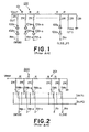
- Fig. 1 One of the conventional voltage-output type D/A converters is shown in Fig. 1.
- This n-bit D/A converter 100 comprises an R-2R ladder network 101 and n groups of serially connected inverters 102 and 103. N-bit digital input data is applied to input terminals IN n-1 to IN O , and each bit of the input data is supplied to the 2R corresponding resistor of the ladder network 101 through the corresponding inverters 102 and 103.
- the inverters 103 outputs a voltage equal to V DD as a logical "1" and outputs a ground voltage as a logical "0", and an output voltage V OUT of this D/A converter 1 00 is taken from the junction point of the 2R and R resistors of the MSB (most significant bit) stage of the ladder network 101 through an output terminal OUT.
- the ladder network 101 is provided with a 2 -1- bit stage (the stage one bit lower than the 2 0- bit stage or the LSB stage) whose 2R resistor is biased by a voltage V DD . With this D/A converter, an analog voltage V OUT proportional to the value of the digital input data appears at the output terminal OUT.
- Fig. 2 shows one example of the conventional current-output type D/A converters.
- This D/A converter 200 comprises an R-2R ladder network 201 and double-pole analog switches SW n-1 to SW 0 .
- Each of the analog switches SW n-1 to SW 0 may be composed of a pair of field effect transistors complementarily connected to each other.
- the junction point of the R and 2R registers of the MSB stage of the R-2R ladder network 201 is supplied with a reference voltage of V REF .
- N-bit digital input data is applied to input terminals IN n-1 to IN 0 , and the switches SW n-1 to SW 0 are controlled by the respective bits of the digital input data.
- An analog output signal in the form of current is taken from a pair of output terminals I OUT1 and I OUT2 , the output terminal I OUT1 being connected to one of the contacts of each of the switches SW n-1 to SW O and the output terminal I OUT2 being connected to the other of the contacts of each of the switches SW n-1 to SW O .
- the above method (a) is disadvantageous in that it requires an expensive trimming apparatus and the skilled operation thereof. This increases the manufacturing cost of - the D/A converter.
- the method (b) is disadvantageous in that the D/A converter must be associated with a memory circuit and a precise reference voltage source and therefore becomes expensive and large in size.
- the correction operation must be carried out periodically, for example, at a time interval of about ten minutes, so that the D/A converter is not easy to use.
- a digital-to-analog converter comprising digital-to-analog converting means for converting multi-bit digital input data into an analog output signal which is proportional in amount to said digital input data, said digital-to-analog converter characterized by the provision of error correction circuit means operatively connected to said digital-to-analog converting means for shifting said analog output signal by a predetermined amount in accordance with a preselected bit of said digital input data.
- the error correction circuit means shifts said analog output signal selectively by one of a plurality of predetermined amounts in accordance with the preselected bit of said digital input data.
- the preselected bit is preferably the most significant bit of said digital input data.
- the error correction circuit means may comprise enabling circuit means responsive to a specific state - of said bit of said digital input data for generating an enabling signal and signal generating means responsive to said enabling signal for generating an analog signal whose amount is a 2- N (N is an integer) magnification of that amount of said analog output signal which corresponds to the least significant bit of said digital input data, said generated analog signal being fed to said digital-to-analog converting means to cause said analog output signal to be shifted by the amount of said generated analog signal.
- the error correction circuit means may be modified to comprise enabling circuit means responsive to a specific state of said bit of said digital input data for generating an enabling signal; an input terminal for receiving a selection signal; and analog signal generating means responsive to said enabling and selection signals for selectively generating one of a plurality of analog signals whose amounts are 2- N (N are integers) magnifications of that amount of said analog output signal which corresponds to the least significant bit of said digital input data, said selectively generated analog signal being fed to said digital-to-analog converting means to cause said analog output signal to be shifted by the amount of said selectively generated analog signal.
- Fig. 3 shows a D/A converter 300 provided in accordance with the present invention.
- This D/A converter 300 comprises, similarly to the conventional D/A converter 100 shown in Fig. 1, n-stage resistor ladder network 101 comprising resistors having values R and 2R and connected as seen in Fig. 1, n groups of serially connected inverters 102 and 103 and input terminals IN n-1 to IN O .
- the ladder network 101 and the inverters 102 and 103 constitute a digital-to-analog converting section 104 of this D/A converter 300.
- N-bit binary digital input data is supplied to the input terminals IN n-1 to IN O , wherein the MSB of the input data is supplied to the input terminal IN n-1 .
- This D/A converter 300 further comprises an exclusive-OR gate (hereinafter referred to as "EXOR gate”) 301 whose one input terminal is connected to the input terminal IN n-1 .
- the other input terminal of the EXOR gate 301 is connected to an input terminal TO to which a signal MS is applied to select a mode of error correction as more fully described later.
- An output terminal of the EXOR gate 301 is connected to an input terminal of an inverter 302 and also connected to one input terminals of AND gates 303 and 304.
- the other input terminals of the AND gates 303 and 304 are connected to input terminals T1 and T2, respectively.
- Output terminals of the inverter 302 and AND gate 303 are connected to input terminals of an OR gate 305.
- An output terminal of the OR gate 305 is connected to an input terminal of an inverter 306 which outputs a voltage equal to V DD as a logical "1" and outputs a ground level signal as a logical "0".
- An output terminal of the inverter 306 is connected to one terminal of a resistor 307 having a resistance value of 2R, and the other terminal of the resistor 307 is connected to one terminal of the R resister of the LSB stage of the ladder network 101, that is, one terminal end of the ladder network 101 on the LSB stage.
- An output terminal of the AND gate 304 is connected to an input terminal of an inverter 308 which outputs a voltage equal to V DD as a logical "1" and outputs a ground level signal as a logical "0".
- An output terminal of the inverter 308 is connected to one terminal of a resistor 308 of a resistance value of 2R, the other terminal of which is connected to the one terminal end of the ladder network 101.
- the inverter 302, the AND gates 303 and 304 and the OR gate 305 cooperate with the inverters 306 and 308 and the resistors 307 and 309 to form an error correction circuit 310 of this D/A converter 300.
- the circuit shown in Fig. 3 is equivalent to that shown in Fig. 1.
- the resistance of the error correction circuit 310 viewed from the ladder network 101 becomes equal to R, so that, the circuit shown in Fig. 3 becomes equivalent to that shown in Fig 1 with the bias to the 2- 1- bit stage thereof being changed from the voltage V DD to the ground level.
- the output voltage V OUT in this case is always lower than that of the circuit shown in Fig. 1 by a voltage equal to V LSB /2, the voltage V LSB being a voltage corresponding to the LSB or the 2 0- bit of the input data.
- the output voltage V OUT of the D/A converter 300 shown in Fig. 3 can be shifted or offset selectively by one of the three different amounts of voltage, namely, zero, + V LSB /2 and - V LSB /2.
- the selection of the shift amount of voltage is made in accordance with a signal S0 outputted from the EXOR gate 301, a signal S1 applied to the input terminal T1 and a signal S2 applied to the input terminal T2, as shown in Table 1.
- the amount of shift of the output voltage V OUT suitable for canceling the error is first determined. Then, the states of the signals S1, S2 and SO are determined so that the above shift amount is selected at the error correction circuit 310. In this case, if the signal MS applied to the input terminal TO is set to "1", the signal SO becomes “1” when the MSB of the input data is "0". On the other hand, if the signal MS is set to "0", the signal SO becomes "1" when the MSB of the input data is "1".
- the D/A converter 300 shown in Fig. 3 is so arranged that the correction is carried - out in accordance with the state of the MSB of the input data.
- the reason for this is that the conversion error of the MSB is generally the largest. However, in the case where the conversion error of a bit of the input data other than the MSB thereof is the largest, the correction may be made in accordance with that bit.
- Fig. 4 shows a modified D/A converter 400 which differs from the D/A converter 300 shown in Fig. 3 in that an error correction circuit 410 substitutes for the error correction circuit 310.
- This error correction circuit 410 comprises resistors 416 and 417 each having a resistance value of R and connected to the R resistor of the LSB stage of the R-2R ladder network 101, resistors 418 and 419 each having a resistance value of 2R and connected to the resister 416, resistors 420 and 421 each having a resistance value of 2R and connected to the resister 417, inverters 422 to 425 whose output terminals are connected respectively to resistors 418 to 421, and inverters 426 and 427 whose output terminals are connected respectively to input terminals of the inverters 423 and 424.
- the error correction circuit 410 also comprises inverters 428 and 429 whose input terminals are connected to input terminals T4 and T3, respectively. Output terminals of the inverters 428 and 429 are connected to first and third input terminals of an AND gate 430 whose second input terminal is supplied with the signal S0. Output terminal of the AND gate 430 is connected to an input terminal of the inverter 426 and a first input terminal of an OR gate 434 whose second input terminal is connected to an input terminal T5.
- the error correction circuit 410 further comprises a three-input AND gate 432 whose first to third input terminals are connected respectively to the input terminals T5 and T4 and the output terminal of the EXOR gate 301, and a two-input AND gate 433 whose first and second input terminals are connected respectively to the input terminal T3 and the output terminal of the EXOR gate 301.
- An output terminal of the AND gate 432 is connected to a first input terminal of an AND gate 431 whose second input terminal is connected to an output terminal of the AND gate 433.
- An output terminal of the AND gate 431 is connected to an input terminal of the inverter 427, and the output terminal of the AND gate 433 is connected to an input terminal of the inverter 425.
- the input terminals T3 to T5 are supplied with selection signals S3 to S5, respectively.
- the output voltage V OUT at the output terminal OUT can be shifted selectively by one of five different amounts of voltage, namely, zero, + V LSB /2, - V LSB / 2, + V LSB /4 and - V LSB /4 in accordance with the states of the signal SO and the signals S3 to S5, as shown in table 2.
- the inverter 422 outputs the voltage V DD
- the inverters 423 to 425 output the ground level signals.
- the inverters 422 to 424 output the voltage V DD
- the inverter 425 outputs the ground level signal.
- the circuit of Fig. 4 becomes equivalent to the circuit of Fig. 1 with the bias to the 2- 2 -bit stage thereof applied, so that the shift amount of the output voltage V OUT is rendered + V LSB /4.
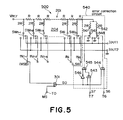
- Fig. 5 shows a further modified D/A converter 500 of the current-output type which differs from the D/A converter 200 of Fig. 2 in that an EXOR gate 301 and an error correction circuit 540 are provided.
- the R-2R ladder network 201 and the switches SW n-1 to SW O constitute a digital-to-analog converting section 204 of this D/A converter 500.
- the EXOR gate 301 is connected to the data input terminals IN n-1 at one input terminal thereof and connected to the input terminal TO at the other input terminal thereof.
- the output terminal of the EXOR gate 301 is connected to an input terminal of an inverter 546 and also connected to one input terminals of AND gates 543 and 544.
- the other input terminals of the AND gates 543 and 544 are connected to input terminals T7 and T6, respectively. These input terminals T6 and T7 are supplied respectively with selection signals S6 and S7.
- Output terminals of the inverter 546 and AND gate 543 are connected to input terminals of an OR gate 545.
- the one terminal end of the R-2R ladder network 201 on the LSB side thereof that is, the one terminal of the R resistor of the LSB stage of the ladder network 201, is connected to one terminals of resistors 541 and 542 each having a resistance value of 2R.
- the other terminals of the resistors 541 and 542 are connected respectively to two-pole analog switches 547 and 548, each of which may be composed of a pair of field effect transistors complementarily connected to each other.
- An output signal of the OR gate 545 is supplied to the switch 547 in such a manner that the other terminal of the resistor 541 is grounded when the OR gate 545 outputs a "0" signal and that the other terminal of the resistor 541 is connected to the output terminal I OUT1 when the AND gate 545 outputs a "1" signal.
- an output signal of the AND gate 544 is supplied to the switch 548 in such a manner that the other terminal of the resistor 542 is grounded when the AND gate 544 outputs a "0" signal and that the other terminal of the resistor 542 is connected to the output terminal I OUT1 when the AND gate 544 outputs a "1" signal.
- the error correction circuit 540 described above is also so arranged that the correction is carried out in accordance with the state of the MSB of the input data. However, in the case where the conversion error of a bit of the input data other than the MSB is the largest, the error correction circuit 540 may be modified so that the correction is made in accordance with that bit. Furthermore, if the correction need be made over a plurality of bits of the input data, a plurality of correction circuits 540 each operatively connected to a respective one of the plurality of bits may be provided.
Landscapes
- Engineering & Computer Science (AREA)
- Theoretical Computer Science (AREA)
- Analogue/Digital Conversion (AREA)
Applications Claiming Priority (2)
| Application Number | Priority Date | Filing Date | Title |
|---|---|---|---|
| JP59212384A JPS6190521A (ja) | 1984-10-09 | 1984-10-09 | デジタル・アナログ変換器 |
| JP212384/84 | 1984-10-09 |
Publications (2)
| Publication Number | Publication Date |
|---|---|
| EP0177909A2 true EP0177909A2 (fr) | 1986-04-16 |
| EP0177909A3 EP0177909A3 (fr) | 1988-12-14 |
Family
ID=16621683
Family Applications (1)
| Application Number | Title | Priority Date | Filing Date |
|---|---|---|---|
| EP85112619A Withdrawn EP0177909A3 (fr) | 1984-10-09 | 1985-10-04 | Convertisseur numérique-analogique |
Country Status (2)
| Country | Link |
|---|---|
| EP (1) | EP0177909A3 (fr) |
| JP (1) | JPS6190521A (fr) |
Cited By (3)
| Publication number | Priority date | Publication date | Assignee | Title |
|---|---|---|---|---|
| EP0325378A2 (fr) * | 1988-01-21 | 1989-07-26 | Advanced Micro Devices, Inc. | Convertisseur numérique-analogique |
| EP0414593A2 (fr) * | 1989-08-19 | 1991-02-27 | Fujitsu Limited | Convertisseur numérique-analogique à réseau résistif en échelle |
| EP0660529A1 (fr) * | 1993-12-27 | 1995-06-28 | Mitsubishi Denki Kabushiki Kaisha | Circuit de convertisseur numérique-analogique |
Citations (2)
| Publication number | Priority date | Publication date | Assignee | Title |
|---|---|---|---|---|
| GB2022347A (en) * | 1978-06-01 | 1979-12-12 | Bendix Corp | Method and apparatus for conversion of signal information between analog and digital forms |
| GB2093297A (en) * | 1981-01-28 | 1982-08-25 | Victor Company Of Japan | D/a converting circuit having two d/a converters |
-
1984
- 1984-10-09 JP JP59212384A patent/JPS6190521A/ja active Pending
-
1985
- 1985-10-04 EP EP85112619A patent/EP0177909A3/fr not_active Withdrawn
Patent Citations (2)
| Publication number | Priority date | Publication date | Assignee | Title |
|---|---|---|---|---|
| GB2022347A (en) * | 1978-06-01 | 1979-12-12 | Bendix Corp | Method and apparatus for conversion of signal information between analog and digital forms |
| GB2093297A (en) * | 1981-01-28 | 1982-08-25 | Victor Company Of Japan | D/a converting circuit having two d/a converters |
Non-Patent Citations (3)
| Title |
|---|
| IBM TECHNICAL DISCLOSURE BULLETIN, vol. 17, no. 5, October 1974, pages 1383-1384, New York, US; F. MADDENS et al.: "Digital-to-analog converter for low-level PCM signals" * |
| NEW ELECTRONICS, vol. 16, no. 2, 25th January 1983, pages 92-93, London, GB; J. MULLEN: "Specifying and using the digital-to-analogue converter" * |
| WESCON TECHNICAL PAPER, vol. 26, September 1982, pages 1-9, Hollywood, US; K. MAIO et al.: "A 16-bit resolution single-chip DAC for audio playback" * |
Cited By (6)
| Publication number | Priority date | Publication date | Assignee | Title |
|---|---|---|---|---|
| EP0325378A2 (fr) * | 1988-01-21 | 1989-07-26 | Advanced Micro Devices, Inc. | Convertisseur numérique-analogique |
| EP0325378A3 (fr) * | 1988-01-21 | 1992-02-26 | Advanced Micro Devices, Inc. | Convertisseur numérique-analogique |
| EP0414593A2 (fr) * | 1989-08-19 | 1991-02-27 | Fujitsu Limited | Convertisseur numérique-analogique à réseau résistif en échelle |
| EP0414593A3 (en) * | 1989-08-19 | 1993-05-12 | Fujitsu Limited | Digital-to-analog converter having a ladder type resistor network |
| EP0660529A1 (fr) * | 1993-12-27 | 1995-06-28 | Mitsubishi Denki Kabushiki Kaisha | Circuit de convertisseur numérique-analogique |
| US5602552A (en) * | 1993-12-27 | 1997-02-11 | Mitsubishi Denki Kabushiki Kaisha | D/A converter capable of disabling the output |
Also Published As
| Publication number | Publication date |
|---|---|
| JPS6190521A (ja) | 1986-05-08 |
| EP0177909A3 (fr) | 1988-12-14 |
Similar Documents
| Publication | Publication Date | Title |
|---|---|---|
| US4638303A (en) | Digital-analog converter | |
| US4533903A (en) | Analog-to-digital converter | |
| US4316178A (en) | Digital-to-analog conversion system with compensation circuit | |
| US4636772A (en) | Multiple function type D/A converter | |
| US4338592A (en) | High accuracy digital-to-analog converter and transient elimination system thereof | |
| US4973979A (en) | Circuit and method for converting digital signal into corresponding analog signal | |
| JP3130528B2 (ja) | ディジタル・アナログ変換器 | |
| US4695826A (en) | High accuracy digital-to-analog converter having symmetrical current source switching | |
| US5617091A (en) | Resistance ladder, D-A converter, and A-D converter | |
| EP0298493B1 (fr) | Convertisseur analogique-numérique à approximations successives | |
| EP0418184B1 (fr) | Convertisseur symétrique doublement numérique-analogique | |
| US4896157A (en) | Digital to analog converter having single resistive string with shiftable voltage thereacross | |
| EP0262664B1 (fr) | Convertisseur analogique numérique | |
| US4665381A (en) | Digital-to-analog converter | |
| KR20020034832A (ko) | 디지털/아날로그 변환 장치 | |
| EP0177909A2 (fr) | Convertisseur numérique-analogique | |
| JP2780992B2 (ja) | サーモメータ・コードまたはサーキュラー・コードに適したエラー訂正電子回路 | |
| EP0782790B1 (fr) | Convertisseur analogique/numerique permettant de generer un code de gray numerique a n bits | |
| US5264851A (en) | A/D converter utilizing a first reference voltage divider and level shifting of a second voltage divider by input signal | |
| EP0200970A2 (fr) | Convertisseur numérique-analogique | |
| US5629702A (en) | Analog to digital converter | |
| EP0681372B1 (fr) | Circuit de conversion numérique-analogique et dispositif de conversion analogique-numérique utilisant ledit circuit | |
| EP0090667B1 (fr) | Convertisseur numérique-analogique à sommation de courants | |
| EP0121234B1 (fr) | Décodeur pour convertisseur N/A | |
| US4057795A (en) | Analog-to-digital encoder |
Legal Events
| Date | Code | Title | Description |
|---|---|---|---|
| PUAI | Public reference made under article 153(3) epc to a published international application that has entered the european phase |
Free format text: ORIGINAL CODE: 0009012 |
|
| AK | Designated contracting states |
Kind code of ref document: A2 Designated state(s): DE GB NL |
|
| 17P | Request for examination filed |
Effective date: 19860902 |
|
| RAP1 | Party data changed (applicant data changed or rights of an application transferred) |
Owner name: YAMAHA CORPORATION |
|
| PUAL | Search report despatched |
Free format text: ORIGINAL CODE: 0009013 |
|
| AK | Designated contracting states |
Kind code of ref document: A3 Designated state(s): DE GB NL |
|
| STAA | Information on the status of an ep patent application or granted ep patent |
Free format text: STATUS: THE APPLICATION IS DEEMED TO BE WITHDRAWN |
|
| 18D | Application deemed to be withdrawn |
Effective date: 19890502 |
|
| RIN1 | Information on inventor provided before grant (corrected) |
Inventor name: TAKAHASHI, TOSHIYUKI Inventor name: OGATA, TAKASHI Inventor name: KOHDAKA, TAKAYUKI Inventor name: ISHIDA, KATSUHIKO |