EP0177115B1 - Dual ion beam deposition of amorphous semiconductor films - Google Patents
Dual ion beam deposition of amorphous semiconductor films Download PDFInfo
- Publication number
- EP0177115B1 EP0177115B1 EP85302833A EP85302833A EP0177115B1 EP 0177115 B1 EP0177115 B1 EP 0177115B1 EP 85302833 A EP85302833 A EP 85302833A EP 85302833 A EP85302833 A EP 85302833A EP 0177115 B1 EP0177115 B1 EP 0177115B1
- Authority
- EP
- European Patent Office
- Prior art keywords
- target
- ions
- process according
- sputtering
- ion
- Prior art date
- Legal status (The legal status is an assumption and is not a legal conclusion. Google has not performed a legal analysis and makes no representation as to the accuracy of the status listed.)
- Expired
Links
Images
Classifications
-
- H—ELECTRICITY
- H10—SEMICONDUCTOR DEVICES; ELECTRIC SOLID-STATE DEVICES NOT OTHERWISE PROVIDED FOR
- H10P—GENERIC PROCESSES OR APPARATUS FOR THE MANUFACTURE OR TREATMENT OF DEVICES COVERED BY CLASS H10
- H10P14/00—Formation of materials, e.g. in the shape of layers or pillars
- H10P14/20—Formation of materials, e.g. in the shape of layers or pillars of semiconductor materials
- H10P14/29—Formation of materials, e.g. in the shape of layers or pillars of semiconductor materials characterised by the substrates
- H10P14/2901—Materials
-
- C—CHEMISTRY; METALLURGY
- C23—COATING METALLIC MATERIAL; COATING MATERIAL WITH METALLIC MATERIAL; CHEMICAL SURFACE TREATMENT; DIFFUSION TREATMENT OF METALLIC MATERIAL; COATING BY VACUUM EVAPORATION, BY SPUTTERING, BY ION IMPLANTATION OR BY CHEMICAL VAPOUR DEPOSITION, IN GENERAL; INHIBITING CORROSION OF METALLIC MATERIAL OR INCRUSTATION IN GENERAL
- C23C—COATING METALLIC MATERIAL; COATING MATERIAL WITH METALLIC MATERIAL; SURFACE TREATMENT OF METALLIC MATERIAL BY DIFFUSION INTO THE SURFACE, BY CHEMICAL CONVERSION OR SUBSTITUTION; COATING BY VACUUM EVAPORATION, BY SPUTTERING, BY ION IMPLANTATION OR BY CHEMICAL VAPOUR DEPOSITION, IN GENERAL
- C23C14/00—Coating by vacuum evaporation, by sputtering or by ion implantation of the coating forming material
- C23C14/0021—Reactive sputtering or evaporation
- C23C14/0036—Reactive sputtering
- C23C14/0047—Activation or excitation of reactive gases outside the coating chamber
- C23C14/0052—Bombardment of substrates by reactive ion beams
-
- C—CHEMISTRY; METALLURGY
- C23—COATING METALLIC MATERIAL; COATING MATERIAL WITH METALLIC MATERIAL; CHEMICAL SURFACE TREATMENT; DIFFUSION TREATMENT OF METALLIC MATERIAL; COATING BY VACUUM EVAPORATION, BY SPUTTERING, BY ION IMPLANTATION OR BY CHEMICAL VAPOUR DEPOSITION, IN GENERAL; INHIBITING CORROSION OF METALLIC MATERIAL OR INCRUSTATION IN GENERAL
- C23C—COATING METALLIC MATERIAL; COATING MATERIAL WITH METALLIC MATERIAL; SURFACE TREATMENT OF METALLIC MATERIAL BY DIFFUSION INTO THE SURFACE, BY CHEMICAL CONVERSION OR SUBSTITUTION; COATING BY VACUUM EVAPORATION, BY SPUTTERING, BY ION IMPLANTATION OR BY CHEMICAL VAPOUR DEPOSITION, IN GENERAL
- C23C14/00—Coating by vacuum evaporation, by sputtering or by ion implantation of the coating forming material
- C23C14/22—Coating by vacuum evaporation, by sputtering or by ion implantation of the coating forming material characterised by the process of coating
- C23C14/34—Sputtering
- C23C14/46—Sputtering by ion beam produced by an external ion source
-
- H—ELECTRICITY
- H10—SEMICONDUCTOR DEVICES; ELECTRIC SOLID-STATE DEVICES NOT OTHERWISE PROVIDED FOR
- H10P—GENERIC PROCESSES OR APPARATUS FOR THE MANUFACTURE OR TREATMENT OF DEVICES COVERED BY CLASS H10
- H10P14/00—Formation of materials, e.g. in the shape of layers or pillars
- H10P14/20—Formation of materials, e.g. in the shape of layers or pillars of semiconductor materials
- H10P14/22—Formation of materials, e.g. in the shape of layers or pillars of semiconductor materials using physical deposition, e.g. vacuum deposition or sputtering
-
- H—ELECTRICITY
- H10—SEMICONDUCTOR DEVICES; ELECTRIC SOLID-STATE DEVICES NOT OTHERWISE PROVIDED FOR
- H10P—GENERIC PROCESSES OR APPARATUS FOR THE MANUFACTURE OR TREATMENT OF DEVICES COVERED BY CLASS H10
- H10P14/00—Formation of materials, e.g. in the shape of layers or pillars
- H10P14/20—Formation of materials, e.g. in the shape of layers or pillars of semiconductor materials
- H10P14/34—Deposited materials, e.g. layers
- H10P14/3402—Deposited materials, e.g. layers characterised by the chemical composition
- H10P14/3404—Deposited materials, e.g. layers characterised by the chemical composition being Group IVA materials
- H10P14/3411—Silicon, silicon germanium or germanium
-
- H—ELECTRICITY
- H10—SEMICONDUCTOR DEVICES; ELECTRIC SOLID-STATE DEVICES NOT OTHERWISE PROVIDED FOR
- H10P—GENERIC PROCESSES OR APPARATUS FOR THE MANUFACTURE OR TREATMENT OF DEVICES COVERED BY CLASS H10
- H10P14/00—Formation of materials, e.g. in the shape of layers or pillars
- H10P14/20—Formation of materials, e.g. in the shape of layers or pillars of semiconductor materials
- H10P14/34—Deposited materials, e.g. layers
- H10P14/3438—Doping during depositing
- H10P14/3441—Conductivity type
- H10P14/3442—N-type
-
- H—ELECTRICITY
- H10—SEMICONDUCTOR DEVICES; ELECTRIC SOLID-STATE DEVICES NOT OTHERWISE PROVIDED FOR
- H10P—GENERIC PROCESSES OR APPARATUS FOR THE MANUFACTURE OR TREATMENT OF DEVICES COVERED BY CLASS H10
- H10P14/00—Formation of materials, e.g. in the shape of layers or pillars
- H10P14/20—Formation of materials, e.g. in the shape of layers or pillars of semiconductor materials
- H10P14/34—Deposited materials, e.g. layers
- H10P14/3438—Doping during depositing
- H10P14/3441—Conductivity type
- H10P14/3444—P-type
Definitions
- Amorphous semiconductor films having a sufficiently small density of localized states have been recognized as having many potential applications, including in photovoltaic devices. Hydrogen and fluorine have been recognized as effective in reducing the density of localized states, i.e., passivating, amorphous silicon films. With respect to hydrogen passivation of silicon, it has been found that the particular coordination of the hydrogen atoms with silicon atoms in hydrogenated amorphous silicon films (a-Si:H) has a dramatic effect on the electronic properties of those films. Films having the most desired electronic characteristics have large silicon monohydride concentrations relative to the concentration of polyhydrides. In fact, for electronic device quality material it is desired that only silicon monohydrides be present and that silicon polyhydrides be entirely absent from a-Si:H films.
- hydrogenated amorphous silicon has a measured band gap energy of 1.7 to 1.8 eV meaning no electrical charge carriers can be generated in those films by photons having an energy less than that band gap energy. Therefore a significant amount of solar energy cannot be converted to electrical energy by amorphous, hydrogenated silicon films.
- band gap energy of a film is too low, the efficiency of the semiconductor film in generating charge carriers in response to incoming photons is reduced.
- semiconductor materials have band gap energies lower than that of amorphous silicon, but are unsuited for photovoltaic cells for numerous reasons, including the difficulty and expense of preparation.
- An ideal band gap energy, compromising efficiency of charge carrier generation and responsiveness to the energy range of photons present in solar illumination, is about 1.4 eV.
- alloys of elemental semiconductors i.e., compound semiconductors, having band gap energies intermediate those of the constituent elements can be prepared.
- single crystal alloys of germanium and silicon have band gap energies between their elemental values (0.72 eV and 1.1 eV, respectively) depending upon the relative proportions of germanium and silicon in the alloy.
- the same band gap energy grading observed in crystalline alloys occurs in passivated amorphous compound semiconductor films, but amorphous semiconductor alloy films having satisfactory electronic properties have been difficult to prepare.
- the problem of controlling the type of hydrogen-semiconductor bonding to produce electronic quality amorphous silicon and amorphous compound semiconductor films by sputtering is solved.
- Control of the bonding to maximize monohydride concentration relative to the polyhydride concentration is achieved by use of separate sputtering ion and hydrogen ion beams both directed at the sputtering target.
- the use of different beams permits independent control of the energies of the two types of ions.
- the type of bonds formed between the semiconductor ions and passivating ions can be controlled.
- the deposited films may be doped by injecting a gaseous dopant, such as phosphine or diborane, into the source or sources producing the passivating ion beams.
- a gaseous dopant such as phosphine or diborane
- the deposition process may be enhanced by illuminating the substrate with ultraviolet light, by heating the substrate and/or by bombarding the substrate with ions or electrons during the deposition.
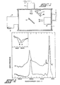
- FIG. 1 Apparatus for carrying out one embodiment of the inventive process is shown schematically in Fig. 1.
- a vacuum chamber 1 is evacuated by a vacuum system 3.
- a vacuum system 3 In our work we used a steel vacuum chamber 48 cm in diameter pumped by a liquid nitrogen-trapped diffusion pump having an ultimate pressure of 6.66 ⁇ 10 -5 pascal.
- Chamber 1 is fitted with a first ion source 5 that can produce an ion beam within the chamber.
- Ion source 5 includes a gas inlet 7 which in our work was connected to a source of argon.
- a second ion source 9 is also fitted to chamber 1 to produce a second ion beam.
- Ion source 9 has a source 11 of a passivating gas connected to it for production of a beam of passivating ions effective in passivating localized states in amorphous semiconductor films.
- a passivating gas We used hydrogen as a passivating gas, but fluorine and other atomic species are also known to be effective.
- ion sources 5 and 9 are conventional Kaufman type ion sources in which a plasma is created in the gas entering the source.
- the ions extracted from the gas in the plasma are directed out of the source and accelerated by an accelerator grid charged with a negative potential.
- a second or screen grid may also be present to suppress secondary emissions from the accelerator grid.
- Argon was used with source 5 to produce relatively heavy ions that are effective in sputtering a silicon or other elemental semiconductor target. Other gases producing relatively heavy ions may be used instead of argon.
- dual graphite grids were used to accelerate the argon ion beam and screen the accelerator grid.
- Ion source 9 may use a graphite grid or, if the sputtering potential of the gas used is low, as with hydrogen, a metal grid may be used.
- a sputtering target 13 is mounted by conventional means.
- the ion beams from sources 5 and 9 are directed to impinge on target 13.
- sputter target 13 was a 12.5 cm diameter, 99.9999% pure silicon wafer. That target was water-cooled by conventional means.
- One or more substrates 15 are mounted within chamber 1 opposing target 13 to collect the material sputtered from it. Substrates 15 are remotely placed to avoid being sputtered themselves and to avoid collection of undesired sputtering products. Substrates 15 may be heated by a thermal source such as quartz lamps 17. In our apparatus, three substrates were used: fused silica, 7059 Corning glass and single crystal silicon. Substrates may also be metallic such as stainless steel. The substrates were mounted against a copper backing plate to spread heat evenly. The backing plate was mounted in a stainless steel holder.
- chamber 1 was evacuated to 1.33 to 2.7x10- 4 pascal and the temperatures of the substrates were allowed to stabilize for at least one hour. All gases delivered to the ion sources were research grade and the gas lines were purged for 15 minutes before sputtering began. Flow rates to the ion sources were adjusted to produce partial argon and hydrogen pressures of 2.3x10- 2 and 8.8x10⁻² pascal, respectively. This hydrogen pressure corresponded to a flow rate of 20 sccm. Sputtered films were cooled to at least 75°C before the venting of chamber 1. Film thicknesses ranged between 0.7 and 1 micrometers and were measured by profilometer.
- the type of hydrogen bonding in the films was determined from their Fourier transform infrared (FTIR) absorption spectra.
- Atomic hydrogen content was calculated from the spectra measured in the vicinity of 640 cm- 1 using the method of Brodsky, et al. published in Physical Review B16, 3556 (1977).
- the currents of the ion beams (argon: 20, 35, 50 mA; hydrogen: 20, 40, 60 mA), and the hydrogen ion beam energy (100, 150, 200 eV) were varied.
- the substrates instead of the target, were bombarded with hydrogen ions and, in some of those tests, krypton was mixed with hydrogen in the second ion source.
- the substrates were illuminated with ultraviolet light.
- the substrate temperature 100, 200, 300°C was also varied.
- the hydrogenated, elemental amorphous silicon films deposited by the inventive technique are of good physical quality. They are smooth and clear, ranging from red to yellow in color. No columnar growth was observed in scanning electron microscope examination of fractured samples, even after etching in potassium hydroxide.
- Fig. 2 shows representative plots of the measured FTIR absorption spectra for two samples.
- the spectrum curve plotted lower and marked as A was measured from an a-Si:H film prepared according to the invention.
- the upper spectrum curve designated B was measured from an a-Si:H film prepared by directing the hydrogen ion beam of source 9 to strike the substrates instead of the target.
- Absorption lines for silicon monohydride and polyhydrides exist at 2000 and 2090 cm -1 , respectively. The percentage of each bonding configuration was estimated from the relative absorbance maxima of these two lines. Polyhydrides also have bending modes at 840 and 890 cm- 1 and the presence of such lines indicates the presence of polyhydrides.
- the photoconductivity of the films, pp is defined as the difference between the conductivity of films measured under light of intensity of 100 mW/cm 2 , and the conductivity in darkness, PD .
- Fig. 5 the logarithm of the dark conductivity of a hydrogenated elemental amorphous silicon film prepared according to the inventive process is plotted as a function of the reciprocal of temperature. The plot shows a single activation energy further confirming that only monohydrides are present in films prepared according to the invention.
- the inventive process is not limited to use with silicon to produce elemental hydrogenated, amorphous semiconductor films with a reduced density of localized states, but may also be used with other group lVa elements from the periodic table, such as germanium and appropriate passivating atoms, such as hydrogen or fluorine, to produce high quality amorphous semiconducting films.
- the inventive process may be used to deposit compound semiconductor passivated films, that is, films containing an alloy of two or more semiconductor elements, plus passivating atoms for reducing the density of localized states.
- a film having a desired, preselected band gap energy can be produced.
- An apparatus 21 for producing such compound semiconductor passivated films is shown in schematic cross sectional view in Fig. 6.
- Apparatus 21 contains many of the same elements as the apparatus of Fig. 1.
- a vacuum vessel 23 is fitted with two ion sources 25 and 27, which may be conventional Kaufman sources.
- Ion source 25 is supplied with a sputtering gas, such as argon; source 27 is supplied with a passivating gas, such as hydrogen or a halogen.
- the beams from ion sources 25 and 27 are directed toward a single sputter target 29 that is water-cooled.
- Target 29 is composed of a substantially pure alloy of elemental semiconductors such as germanium and silicon.
- Target 29 may be crystalline or polycrystalline.
- the material sputtered from target 29 is collected on a substrate 31 that is located remotely from the ion beams and target to avoid collection of inadvertently sputtered material and to avoid sputtering of the substrate.
- the temperature of substrate 31 may be elevated by a heat source which may be quartz lamps 33.
- a source of ultraviolet light 35 may be used to illuminate substrate 31 and an electron source 37 may bombard substrate 31.
- substrate 31 may be heated, illuminated with ultraviolet light and bombarded with electrons, independently or in any combination, to enhance the deposition process.
- Substrate 31 may be a glass, a semiconductor or a metal such as stainless steel.
- the rate of sputtering of target 29 and the passivating atom content of the sputtered products can be independently controlled.
- this feature of the inventive process is particularly important since it is known that the particular coordination of the hydrogen atoms with the semiconductor atoms in hydrogenated amorphous films has a dramatic effect on the electronic properties of the film.
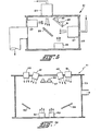
- FIG. 7 Another apparatus 41 for an application of the inventive process is shown in schematic cross-sectional form in Fig. 7.
- a vacuum vessel 23 is fitted with four ion sources 45, 47, 49 and 51.
- Ion sources 45 and 47 are directed at a sputter target 53 which is preferably an elemental semiconductor such as silicon or germanium.
- Ion source 45 is supplied with a sputtering gas, such as argon, to produce a beam of ions that sputter material from target 53.
- Source 47 is supplied with a passivating gas to produce a beam of passivating ions that impinge on target 53.
- Ion sources 49 and 51 are entirely analogous to sources 45 and 47, except that they are directed at another sputter target 55.
- That target 55 is an elemental semiconductor, such as silicon or germanium, different from the composition of target 53.
- the deposited alloy will be composed of the materials comprising the two targets 53 and 55. Both targets are water-eooted and are of high purity.
- the materials sputtered from targets 53 and 55 are collected on a substrate 57.
- Substrate 57 is located remotely from the four ion beams and the two targets to avoid collection of inadvertently sputtered material and to avoid sputtering of the substrate.
- the temperature of the substrate may be elevated by a heat source which may be quartz lamps 59.
- An ultraviolet light source 61 and electron source 63 are also provided to illuminate and bombard substrate 57 during deposition, if desired.
- the substrates may be heated, illuminated with ultraviolet light and bombarded with electrons, or any combination of them to enhance the deposition process.
- the substrate may be a glass, including fused silica, a semiconductor such as silicon, or may be metallic, such as a stainless steel.
- the rate of sputtering of the respective targets, the composition of the deposited alloy film and the passivating atom content of the sputter products can be carefully controlled. This extreme degree of control is of great importance since the alloy composition and, in our work, the content and bonding of the passivating atoms in the film, has a very substantial effect upon the electronic properties of the film.
- compositions of passivated ternary alloys such as Si x Ge 1 - x (H), where x ranges between 0 and 1, can be produced.
- Films deposited according to any of the described embodiments of the inventive process may be doped during deposition by adding a gaseous dopant to the passivating ion beam source.
- Phosphine may be ionized to produce phosphorous ions for preparing n-type material and diborane may be ionized to boron ions for preparing p-type material.
- junction devices such as p-n and p-i-n structures can be formed in the films.
Landscapes
- Chemical & Material Sciences (AREA)
- Chemical Kinetics & Catalysis (AREA)
- Engineering & Computer Science (AREA)
- Materials Engineering (AREA)
- Mechanical Engineering (AREA)
- Metallurgy (AREA)
- Organic Chemistry (AREA)
- Physical Deposition Of Substances That Are Components Of Semiconductor Devices (AREA)
- Physical Vapour Deposition (AREA)
Description
- Amorphous semiconductor films having a sufficiently small density of localized states have been recognized as having many potential applications, including in photovoltaic devices. Hydrogen and fluorine have been recognized as effective in reducing the density of localized states, i.e., passivating, amorphous silicon films. With respect to hydrogen passivation of silicon, it has been found that the particular coordination of the hydrogen atoms with silicon atoms in hydrogenated amorphous silicon films (a-Si:H) has a dramatic effect on the electronic properties of those films. Films having the most desired electronic characteristics have large silicon monohydride concentrations relative to the concentration of polyhydrides. In fact, for electronic device quality material it is desired that only silicon monohydrides be present and that silicon polyhydrides be entirely absent from a-Si:H films.
- Typically, hydrogenated amorphous silicon has a measured band gap energy of 1.7 to 1.8 eV meaning no electrical charge carriers can be generated in those films by photons having an energy less than that band gap energy. Therefore a significant amount of solar energy cannot be converted to electrical energy by amorphous, hydrogenated silicon films. On the other hand, if the band gap energy of a film is too low, the efficiency of the semiconductor film in generating charge carriers in response to incoming photons is reduced. Various semiconductor materials have band gap energies lower than that of amorphous silicon, but are unsuited for photovoltaic cells for numerous reasons, including the difficulty and expense of preparation. An ideal band gap energy, compromising efficiency of charge carrier generation and responsiveness to the energy range of photons present in solar illumination, is about 1.4 eV.
- It is known that alloys of elemental semiconductors, i.e., compound semiconductors, having band gap energies intermediate those of the constituent elements can be prepared. For example, single crystal alloys of germanium and silicon have band gap energies between their elemental values (0.72 eV and 1.1 eV, respectively) depending upon the relative proportions of germanium and silicon in the alloy. The same band gap energy grading observed in crystalline alloys occurs in passivated amorphous compound semiconductor films, but amorphous semiconductor alloy films having satisfactory electronic properties have been difficult to prepare.
- Numerous processes have been employed to produce a-Si:H films, but to date, none have reliably controlled the coordination of passivating atoms with the semiconductor atoms in the films. Among the deposition techniques that have been used are glow discharge and radio frequency and reactive gas sputtering. An example of sputtering using a single ion gun is disclosed in U.S. Patent 4,376,688 to Caesar et al. Dual ion beam sputtering was reported by Coluzza and others in an article "a-Si:H Produced by Double lon-Beam Sputtering" in 59 & 60 Journal of Non-Crystalline Solids, 723-726 (1983). In that article, the authors disclosed directing a sputtering (argon) beam at a silicon target and a passivating beam of (hydrogen) at the substrate on which the sputtered amorphous silicon was condensed. The published results indicated that no improvement was achieved in reliably controlling the amount and form of hydrogen content of the film deposited by the Coluzza et al. dual ion beam sputtering technique.
- In the invention, the problem of controlling the type of hydrogen-semiconductor bonding to produce electronic quality amorphous silicon and amorphous compound semiconductor films by sputtering is solved. Control of the bonding to maximize monohydride concentration relative to the polyhydride concentration is achieved by use of separate sputtering ion and hydrogen ion beams both directed at the sputtering target. The use of different beams permits independent control of the energies of the two types of ions. By controlling the energy of the passivating ions, the type of bonds formed between the semiconductor ions and passivating ions can be controlled.
- The deposited films may be doped by injecting a gaseous dopant, such as phosphine or diborane, into the source or sources producing the passivating ion beams. The deposition process may be enhanced by illuminating the substrate with ultraviolet light, by heating the substrate and/or by bombarding the substrate with ions or electrons during the deposition.
- The invention can be understood more clearly by reference to the drawing figures taken in conjunction with the detailed description that follows.
- Fig. 1 shows in schematic form a cross-sectional view of an apparatus that may be used to deposit elemental semiconductor films according to the invention.
- Fig. 2 shows relative, representative plots of the measured absorption spectra of two elemental semiconductor sample films, one of which was prepared according to the inventive process.
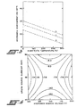
- Fig. 3 is a least squares plot of the measured bonded hydrogen concentration as a function of substrate temperature and hydrogen ion beam current for elemental semiconductor films prepared according to the invention.
- Fig. 4 is a least squares plot of the logarithm of the measured photoconductivity of elemental semiconductor films prepared both according to the inventive process and with substrate bombardment by hydrogen ions for a fixed substrate temperature, as a function of argon ion beam current and hydrogen ion beam voltage.
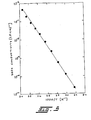
- Fig. 5 is a plot of dark conductivity as a function of the reciprocal of temperature for an elemental semiconductor film prepared according to the inventive process.
- Fig. 6 is a schematic cross-sectional view of an apparatus that may be used to deposit compound semiconductor films according to the invention.
- Fig. 7 is a schematic cross-sectional view of an apparatus that may be used to deposit compound semiconductor films according to the invention.
- Apparatus for carrying out one embodiment of the inventive process is shown schematically in Fig. 1. A
vacuum chamber 1 is evacuated by a vacuum system 3. In our work we used a steel vacuum chamber 48 cm in diameter pumped by a liquid nitrogen-trapped diffusion pump having an ultimate pressure of 6.66×10⁻⁵ pascal.Chamber 1 is fitted with afirst ion source 5 that can produce an ion beam within the chamber. Ionsource 5 includes agas inlet 7 which in our work was connected to a source of argon. A second ion source 9 is also fitted tochamber 1 to produce a second ion beam. Ion source 9 has asource 11 of a passivating gas connected to it for production of a beam of passivating ions effective in passivating localized states in amorphous semiconductor films. We used hydrogen as a passivating gas, but fluorine and other atomic species are also known to be effective. - In a preferred embodiment of the apparatus for performing the inventive process,
ion sources 5 and 9 are conventional Kaufman type ion sources in which a plasma is created in the gas entering the source. The ions extracted from the gas in the plasma are directed out of the source and accelerated by an accelerator grid charged with a negative potential. A second or screen grid may also be present to suppress secondary emissions from the accelerator grid. We used sources 2.5 cm in diameter to form each ion beam. Argon was used withsource 5 to produce relatively heavy ions that are effective in sputtering a silicon or other elemental semiconductor target. Other gases producing relatively heavy ions may be used instead of argon. In our apparatus, dual graphite grids were used to accelerate the argon ion beam and screen the accelerator grid. Ion source 9 may use a graphite grid or, if the sputtering potential of the gas used is low, as with hydrogen, a metal grid may be used. We used a single nickel accelerator grid for a hydrogen ion source. - Within
chamber 1, a sputteringtarget 13 is mounted by conventional means. The ion beams fromsources 5 and 9 are directed to impinge ontarget 13. In our work,sputter target 13 was a 12.5 cm diameter, 99.9999% pure silicon wafer. That target was water-cooled by conventional means. - One or
more substrates 15 are mounted withinchamber 1opposing target 13 to collect the material sputtered from it.Substrates 15 are remotely placed to avoid being sputtered themselves and to avoid collection of undesired sputtering products.Substrates 15 may be heated by a thermal source such asquartz lamps 17. In our apparatus, three substrates were used: fused silica, 7059 Corning glass and single crystal silicon. Substrates may also be metallic such as stainless steel. The substrates were mounted against a copper backing plate to spread heat evenly. The backing plate was mounted in a stainless steel holder. - In our procedure,
chamber 1 was evacuated to 1.33 to 2.7x10⁻⁴ pascal and the temperatures of the substrates were allowed to stabilize for at least one hour. All gases delivered to the ion sources were research grade and the gas lines were purged for 15 minutes before sputtering began. Flow rates to the ion sources were adjusted to produce partial argon and hydrogen pressures of 2.3x10⁻² and 8.8x10⁻² pascal, respectively. This hydrogen pressure corresponded to a flow rate of 20 sccm. Sputtered films were cooled to at least 75°C before the venting ofchamber 1. Film thicknesses ranged between 0.7 and 1 micrometers and were measured by profilometer. The type of hydrogen bonding in the films was determined from their Fourier transform infrared (FTIR) absorption spectra. Atomic hydrogen content was calculated from the spectra measured in the vicinity of 640 cm-1 using the method of Brodsky, et al. published in Physical Review B16, 3556 (1977). - In our work the currents of the ion beams (argon: 20, 35, 50 mA; hydrogen: 20, 40, 60 mA), and the hydrogen ion beam energy (100, 150, 200 eV) were varied. In addition, in some of our tests, the substrates, instead of the target, were bombarded with hydrogen ions and, in some of those tests, krypton was mixed with hydrogen in the second ion source. In some tests, the substrates were illuminated with ultraviolet light. The substrate temperature (100, 200, 300°C) was also varied.
- The hydrogenated, elemental amorphous silicon films deposited by the inventive technique are of good physical quality. They are smooth and clear, ranging from red to yellow in color. No columnar growth was observed in scanning electron microscope examination of fractured samples, even after etching in potassium hydroxide.
- Fig. 2 shows representative plots of the measured FTIR absorption spectra for two samples. The spectrum curve plotted lower and marked as A was measured from an a-Si:H film prepared according to the invention. The upper spectrum curve designated B was measured from an a-Si:H film prepared by directing the hydrogen ion beam of source 9 to strike the substrates instead of the target. Absorption lines for silicon monohydride and polyhydrides exist at 2000 and 2090 cm-1, respectively. The percentage of each bonding configuration was estimated from the relative absorbance maxima of these two lines. Polyhydrides also have bending modes at 840 and 890 cm-1 and the presence of such lines indicates the presence of polyhydrides. Curve B of Fig. 2 clearly shows an increase at 2090 cm-1 that is not present in curve A. Likewise, the polyhydride bending mode lines are clearly present in curve B, but not curve A. From such spectral measurements it was determined that films prepared according to the invention, i.e., in which the hydrogen ion beam was directed at the sputtering target, were free of polyhydrides. The inset in Fig. 2 shows a higher resolution scan in the range from 2000 to 2100 cm-1. These scans show very clearly the presence of the 2090 cm-1 line in sample B indicating the presence of polyhydrides, and its absence in sample A that was prepared according the inventive process.
- The total measured atomic percent of bonded hydrogen in films we prepared is illustrated in Fig. 3. There, a least squares fit of the measured percentage of total bonded hydrogen present in films prepared according to the invention is plotted against substrate temperatures for different hydrogen ion beam currents (a=20 mA, b=40 mA, c=60 mA). In the plotted results, all hydrogen was bound as monohydride regardless of the quantity of hydrogen present.
- The photoconductivity of the films, pp, is defined as the difference between the conductivity of films measured under light of intensity of 100 mW/cm2, and the conductivity in darkness, PD. The photoconductivity of elemental, amorphous silicon films deposited on fused silica substrates both according to the inventive process and with hydrogen ions directed at the substrate, was measured using painted carbon contacts. These contacts were tested and determined to be ohmic. Hydrogen beam voltage, argon beam current and substrate temperature were the most significant variables affecting the measured photoconductivity of films prepared according to both processes. A least squares fit of the logarithm of the measured photoconductivity of films prepared according to both processes at a substrate temperature of 300°C, is plotted in Fig. 4 as a function of argon ion beam current and the voltage used to accelerate the hydrogen ion beam. We found that for the conditions thatwe used that photoconductivity is maximized at a hydrogen ion acceleration voltage of 150 volts and ion current of 35 mA. These conditions appear as a saddle point on the graph of Fig. 4.
- In Fig. 5, the logarithm of the dark conductivity of a hydrogenated elemental amorphous silicon film prepared according to the inventive process is plotted as a function of the reciprocal of temperature. The plot shows a single activation energy further confirming that only monohydrides are present in films prepared according to the invention.
- The characteristics of elemental hydrogenated amorphous silicon films deposited according to the inventive process under varying conditions are listed in Table 1 for
tests Tests 5 and 6 are also listed to show results when the hydrogen beam was directed at the substrates rather than at the sputtering target. In the Table, the following measured test conditions and measured results are listed: argon ion beam current, hydrogen ion beam current, hydrogen ion acceleration voltage, substrate temperature, the direction of the hydrogen passivating ion beam at the (sputtering target or at the substrate), presence or absence of ultraviolet illumination of the substrates, measured percentage of silicon monohydride in the deposited film, atomic percentage of hydrogen in the deposited film, and the measured logarithms of the dark conductivity and of the photoconductivity of the deposited films. The final column in Table 1 lists the activation energy for amorphous hydrogenated elemental silicon films prepared according to'the inventive process as measured by the technique producing the results plotted in Fig. 5. Entries of N.A. mean that no single activation energy was measured and that the measured plot was non-linear. As indicated in the Table, a single activation energy was found for all but one filmn prepared according to the inventive process. Test 9 produced an anomalous, non-linear result having no single activation energy. By contrast, the activation energy plots of films made during hydrogen ion bombardment of the substrates were always non-linear.
- The precise mechanism in the process that produces the desired results is not completely understood. It appears to us that in the deposition of hydrogenated amorphous silicon, silicon polyhydride is formed at the target and that reactive hydrogen, along with silicon, is sputtered onto the substrate. We believe that polyhydide formation in deposited films is primarily the result of large amounts of reactive hydrogen being present at the film surface during film growth. Therefore, conditions that favor polyhydride formation at the sputtering target and reduce the concentration of atomic hydrogen at the substrate, result in an increase of monohydride content in sputtered films.
- The inventive process is not limited to use with silicon to produce elemental hydrogenated, amorphous semiconductor films with a reduced density of localized states, but may also be used with other group lVa elements from the periodic table, such as germanium and appropriate passivating atoms, such as hydrogen or fluorine, to produce high quality amorphous semiconducting films.
- In addition, the inventive process may be used to deposit compound semiconductor passivated films, that is, films containing an alloy of two or more semiconductor elements, plus passivating atoms for reducing the density of localized states. By alloying semiconductor elements, a film having a desired, preselected band gap energy can be produced. An
apparatus 21 for producing such compound semiconductor passivated films is shown in schematic cross sectional view in Fig. 6.Apparatus 21 contains many of the same elements as the apparatus of Fig. 1. Avacuum vessel 23 is fitted with twoion sources Ion source 25 is supplied with a sputtering gas, such as argon;source 27 is supplied with a passivating gas, such as hydrogen or a halogen. The beams fromion sources single sputter target 29 that is water-cooled.Target 29 is composed of a substantially pure alloy of elemental semiconductors such as germanium and silicon.Target 29 may be crystalline or polycrystalline. - The material sputtered from
target 29 is collected on asubstrate 31 that is located remotely from the ion beams and target to avoid collection of inadvertently sputtered material and to avoid sputtering of the substrate. The temperature ofsubstrate 31 may be elevated by a heat source which may bequartz lamps 33. A source ofultraviolet light 35 may be used to illuminatesubstrate 31 and anelectron source 37 may bombardsubstrate 31. During deposition,substrate 31 may be heated, illuminated with ultraviolet light and bombarded with electrons, independently or in any combination, to enhance the deposition process.Substrate 31 may be a glass, a semiconductor or a metal such as stainless steel. - By varying the current and energy of the two ion beams separately, the rate of sputtering of
target 29 and the passivating atom content of the sputtered products can be independently controlled. As noted above, this feature of the inventive process is particularly important since it is known that the particular coordination of the hydrogen atoms with the semiconductor atoms in hydrogenated amorphous films has a dramatic effect on the electronic properties of the film. - Another
apparatus 41 for an application of the inventive process is shown in schematic cross-sectional form in Fig. 7. Avacuum vessel 23 is fitted with fourion sources Ion sources sputter target 53 which is preferably an elemental semiconductor such as silicon or germanium.Ion source 45 is supplied with a sputtering gas, such as argon, to produce a beam of ions that sputter material fromtarget 53.Source 47 is supplied with a passivating gas to produce a beam of passivating ions that impinge ontarget 53.Ion sources sources sputter target 55. Thattarget 55 is an elemental semiconductor, such as silicon or germanium, different from the composition oftarget 53. The deposited alloy will be composed of the materials comprising the twotargets - The materials sputtered from
targets substrate 57.Substrate 57 is located remotely from the four ion beams and the two targets to avoid collection of inadvertently sputtered material and to avoid sputtering of the substrate. The temperature of the substrate may be elevated by a heat source which may bequartz lamps 59. An ultravioletlight source 61 andelectron source 63 are also provided to illuminate and bombardsubstrate 57 during deposition, if desired. As noted for the other application described, the substrates may be heated, illuminated with ultraviolet light and bombarded with electrons, or any combination of them to enhance the deposition process. The substrate may be a glass, including fused silica, a semiconductor such as silicon, or may be metallic, such as a stainless steel. - By varying the currents and energies of the four ion beams used in this application of the inventive process, the rate of sputtering of the respective targets, the composition of the deposited alloy film and the passivating atom content of the sputter products can be carefully controlled. This extreme degree of control is of great importance since the alloy composition and, in our work, the content and bonding of the passivating atoms in the film, has a very substantial effect upon the electronic properties of the film.
- By using either of the two embodiments of the inventive process just described, a continuum of compositions of passivated ternary alloys, such as SixGe1-x(H), where x ranges between 0 and 1, can be produced.
- Films deposited according to any of the described embodiments of the inventive process may be doped during deposition by adding a gaseous dopant to the passivating ion beam source. Phosphine may be ionized to produce phosphorous ions for preparing n-type material and diborane may be ionized to boron ions for preparing p-type material. By changing dopants during deposition, junction devices such as p-n and p-i-n structures can be formed in the films. In the embodiments described for depositing amorphous compound semiconductor films, there is a choice of passivating ion sources and the same dopant need not be supplied to each.
Claims (15)
Applications Claiming Priority (4)
| Application Number | Priority Date | Filing Date | Title |
|---|---|---|---|
| US64720884A | 1984-09-04 | 1984-09-04 | |
| US647208 | 1984-09-04 | ||
| US65316884A | 1984-09-24 | 1984-09-24 | |
| US653168 | 1984-09-24 |
Publications (2)
| Publication Number | Publication Date |
|---|---|
| EP0177115A1 EP0177115A1 (en) | 1986-04-09 |
| EP0177115B1 true EP0177115B1 (en) | 1989-07-19 |
Family
ID=27095110
Family Applications (1)
| Application Number | Title | Priority Date | Filing Date |
|---|---|---|---|
| EP85302833A Expired EP0177115B1 (en) | 1984-09-04 | 1985-04-23 | Dual ion beam deposition of amorphous semiconductor films |
Country Status (4)
| Country | Link |
|---|---|
| EP (1) | EP0177115B1 (en) |
| AU (1) | AU566986B2 (en) |
| DE (1) | DE3571718D1 (en) |
| ES (1) | ES8607422A1 (en) |
Families Citing this family (3)
| Publication number | Priority date | Publication date | Assignee | Title |
|---|---|---|---|---|
| US4673475A (en) * | 1985-06-28 | 1987-06-16 | The Standard Oil Company | Dual ion beam deposition of dense films |
| GB2208390B (en) * | 1987-08-06 | 1991-03-27 | Plessey Co Plc | Thin film deposition process |
| RU2614080C1 (en) * | 2015-12-16 | 2017-03-22 | Общество с ограниченной ответственностью "НТЦ тонкопленочных технологий в энергетике при ФТИ им. А.Ф. Иоффе", ООО "НТЦ ТПТ" | Silicon wafer surface passivation by magnetron sputtering |
Family Cites Families (4)
| Publication number | Priority date | Publication date | Assignee | Title |
|---|---|---|---|---|
| DE1934326A1 (en) * | 1968-10-17 | 1970-08-06 | Inst Elektronische Bauelemente | Multi-beam ion atomization system for the production of thin, uniform or alloyed layers |
| US4376688A (en) * | 1981-04-03 | 1983-03-15 | Xerox Corporation | Method for producing semiconductor films |
| US4416755A (en) * | 1981-04-03 | 1983-11-22 | Xerox Corporation | Apparatus and method for producing semiconducting films |
| JPS59170270A (en) * | 1983-03-15 | 1984-09-26 | Toshiba Corp | Apparatus for forming film |
-
1985
- 1985-04-22 AU AU41464/85A patent/AU566986B2/en not_active Ceased
- 1985-04-23 DE DE8585302833T patent/DE3571718D1/en not_active Expired
- 1985-04-23 EP EP85302833A patent/EP0177115B1/en not_active Expired
- 1985-04-26 ES ES542603A patent/ES8607422A1/en not_active Expired
Also Published As
| Publication number | Publication date |
|---|---|
| ES542603A0 (en) | 1986-05-16 |
| AU4146485A (en) | 1986-03-13 |
| DE3571718D1 (en) | 1989-08-24 |
| AU566986B2 (en) | 1987-11-05 |
| EP0177115A1 (en) | 1986-04-09 |
| ES8607422A1 (en) | 1986-05-16 |
Similar Documents
| Publication | Publication Date | Title |
|---|---|---|
| US4637869A (en) | Dual ion beam deposition of amorphous semiconductor films | |
| US4416755A (en) | Apparatus and method for producing semiconducting films | |
| US4376688A (en) | Method for producing semiconductor films | |
| US4443488A (en) | Plasma ion deposition process | |
| US4336277A (en) | Transparent electrical conducting films by activated reactive evaporation | |
| EP0306297B1 (en) | Pin junction photovoltaic element wherein the I-type semiconductor layer is formed of ZnSe or ZnSeTe containing 1-4 atomic % hydrogen | |
| US4596645A (en) | Reactively-sputtered zinc semiconductor films of high conductivity for heterojunction devices | |
| Moustakas | Studies of thin-film growth of sputtered hydrogenated amorphous silicon | |
| EP0156069B1 (en) | Diamond-like thin film and method for making the same | |
| AU598996B2 (en) | Functional znse:h deposited films | |
| US4926229A (en) | Pin junction photovoltaic element with P or N-type semiconductor layer comprising non-single crystal material containing Zn, Se, H in an amount of 1 to 4 atomic % and a dopant and I-type semiconductor layer comprising non-single crystal Si(H,F) material | |
| JPH0143449B2 (en) | ||
| Boxman et al. | Filtered vacuum arc deposition of semiconductor thin films | |
| US20100065418A1 (en) | Reactive magnetron sputtering for the large-scale deposition of chalcopyrite absorber layers for thin layer solar cells | |
| EP0177115B1 (en) | Dual ion beam deposition of amorphous semiconductor films | |
| EP0104916B1 (en) | Depositing a film onto a substrate including electron-beam evaporation | |
| Yamada et al. | Preparation of doped amorphous silicon films by ionized‐cluster beam deposition | |
| CA1235385A (en) | Hard layer formed by incorporating nitrogen into mo or w metal and method for obtaining this layer | |
| US5501745A (en) | Low temperature method for making a photovoltaic material | |
| Ceasar et al. | Ion beam deposition of a-Si: H | |
| CA1240283A (en) | Dual ion beam deposition of amorphous semiconductor alloy films | |
| JPS6167220A (en) | Method of analyzing double ion beam of amorphous semiconductor film | |
| Maruyama et al. | Thin Films of Amorphous Silicon‐Tin Alloy Prepared by Radio‐Frequency Magnetron Sputtering | |
| Anderson et al. | Activated reactive evaporation of hydrogenated amorphous silicon | |
| Saito et al. | Effects of gallium doping on the properties of amorphous-SiC: H films prepared by magnetron cosputtering |
Legal Events
| Date | Code | Title | Description |
|---|---|---|---|
| PUAI | Public reference made under article 153(3) epc to a published international application that has entered the european phase |
Free format text: ORIGINAL CODE: 0009012 |
|
| AK | Designated contracting states |
Kind code of ref document: A1 Designated state(s): CH DE FR GB IT LI NL |
|
| RAP1 | Party data changed (applicant data changed or rights of an application transferred) |
Owner name: THE STANDARD OIL COMPANY |
|
| 17P | Request for examination filed |
Effective date: 19860924 |
|
| 17Q | First examination report despatched |
Effective date: 19880825 |
|
| GRAA | (expected) grant |
Free format text: ORIGINAL CODE: 0009210 |
|
| AK | Designated contracting states |
Kind code of ref document: B1 Designated state(s): CH DE FR GB IT LI NL |
|
| REF | Corresponds to: |
Ref document number: 3571718 Country of ref document: DE Date of ref document: 19890824 |
|
| ET | Fr: translation filed | ||
| ITF | It: translation for a ep patent filed | ||
| PGFP | Annual fee paid to national office [announced via postgrant information from national office to epo] |
Ref country code: GB Payment date: 19900331 Year of fee payment: 6 |
|
| PGFP | Annual fee paid to national office [announced via postgrant information from national office to epo] |
Ref country code: FR Payment date: 19900416 Year of fee payment: 6 |
|
| PGFP | Annual fee paid to national office [announced via postgrant information from national office to epo] |
Ref country code: DE Payment date: 19900425 Year of fee payment: 6 |
|
| ITTA | It: last paid annual fee | ||
| PGFP | Annual fee paid to national office [announced via postgrant information from national office to epo] |
Ref country code: NL Payment date: 19900430 Year of fee payment: 6 |
|
| PLBE | No opposition filed within time limit |
Free format text: ORIGINAL CODE: 0009261 |
|
| STAA | Information on the status of an ep patent application or granted ep patent |
Free format text: STATUS: NO OPPOSITION FILED WITHIN TIME LIMIT |
|
| 26N | No opposition filed | ||
| PGFP | Annual fee paid to national office [announced via postgrant information from national office to epo] |
Ref country code: CH Payment date: 19900731 Year of fee payment: 6 |
|
| PG25 | Lapsed in a contracting state [announced via postgrant information from national office to epo] |
Ref country code: GB Effective date: 19910423 |
|
| PG25 | Lapsed in a contracting state [announced via postgrant information from national office to epo] |
Ref country code: LI Effective date: 19910430 Ref country code: CH Effective date: 19910430 |
|
| PG25 | Lapsed in a contracting state [announced via postgrant information from national office to epo] |
Ref country code: NL Effective date: 19911101 |
|
| NLV4 | Nl: lapsed or anulled due to non-payment of the annual fee | ||
| GBPC | Gb: european patent ceased through non-payment of renewal fee | ||
| PG25 | Lapsed in a contracting state [announced via postgrant information from national office to epo] |
Ref country code: FR Effective date: 19911230 |
|
| REG | Reference to a national code |
Ref country code: CH Ref legal event code: PL |
|
| PG25 | Lapsed in a contracting state [announced via postgrant information from national office to epo] |
Ref country code: DE Effective date: 19920201 |
|
| REG | Reference to a national code |
Ref country code: FR Ref legal event code: ST |