EP0174151B1 - Verzögertes Triggersystem für ein Digital-Oszilloskop - Google Patents
Verzögertes Triggersystem für ein Digital-Oszilloskop Download PDFInfo
- Publication number
- EP0174151B1 EP0174151B1 EP85306074A EP85306074A EP0174151B1 EP 0174151 B1 EP0174151 B1 EP 0174151B1 EP 85306074 A EP85306074 A EP 85306074A EP 85306074 A EP85306074 A EP 85306074A EP 0174151 B1 EP0174151 B1 EP 0174151B1
- Authority
- EP
- European Patent Office
- Prior art keywords
- trigger
- circuit
- holdoff
- pulse
- signal
- Prior art date
- Legal status (The legal status is an assumption and is not a legal conclusion. Google has not performed a legal analysis and makes no representation as to the accuracy of the status listed.)
- Expired
Links
- 239000003990 capacitor Substances 0.000 claims description 11
- 230000004044 response Effects 0.000 claims description 8
- 238000005070 sampling Methods 0.000 claims description 8
- 238000010586 diagram Methods 0.000 description 5
- 238000000034 method Methods 0.000 description 5
- 230000001960 triggered effect Effects 0.000 description 3
- 238000012797 qualification Methods 0.000 description 2
- 230000000977 initiatory effect Effects 0.000 description 1
- 238000003909 pattern recognition Methods 0.000 description 1
- 230000003252 repetitive effect Effects 0.000 description 1
Images
Classifications
-
- H—ELECTRICITY
- H03—ELECTRONIC CIRCUITRY
- H03K—PULSE TECHNIQUE
- H03K3/00—Circuits for generating electric pulses; Monostable, bistable or multistable circuits
- H03K3/02—Generators characterised by the type of circuit or by the means used for producing pulses
- H03K3/023—Generators characterised by the type of circuit or by the means used for producing pulses by the use of differential amplifiers or comparators, with internal or external positive feedback
-
- G—PHYSICS
- G01—MEASURING; TESTING
- G01R—MEASURING ELECTRIC VARIABLES; MEASURING MAGNETIC VARIABLES
- G01R13/00—Arrangements for displaying electric variables or waveforms
- G01R13/20—Cathode-ray oscilloscopes
- G01R13/22—Circuits therefor
- G01R13/32—Circuits for displaying non-recurrent functions such as transients; Circuits for triggering; Circuits for synchronisation; Circuits for time-base expansion
Definitions
- the present invention relates generally to trigger systems for oscilloscopes, and particularly to a trigger holdoff system for controlling the inhibit/-enable cycle of the acquisition system of a digital oscilloscope.
- an input waveform is sampled at equally spaced time points along the time axis of the waveform, converted to digital data for storage, and displayed on a screen as an amplitude-versus-time waveform. That is, the input signal is sampled in response to a sampling clock and converted to digital data which is stored in a so-called acquisition memory under the control of a time-base control and address generator circuit.
- the input signal is also applied to a trigger generator which generates a trigger signal to be applied to the time-base control circuit.
- the time-base control circuit is enabled under control of a microprocessor and, when triggered, initiates an acquisition cycle to fill an acquisition memory.
- the acquired waveform is transferred to a display memory under control of the microprocessor.
- the microprocessor suitably may also process the waveform data for producing interpolation data, jitter correction and perhaps other waveform refinements, with the processed result being sent to the display memory.
- the microprocessor enables the time-base control circuit again to allow it to respond to another trigger from the trigger generator.
- the acquisition cycle may not begin at the identical trigger point on the input signal because the processing time of the microprocessor varies, depending upon such factors as the kind of process and the number of processes. Therefore, if repetitious acquisition-and-display cycles are employed, the waveform displayed on the screen is unstable. This is particularly noticeable at the higher sweep speeds.
- EP-A1-0 087 608 discloses an example of a circuit suffering from such disadvantages.
- the trigger generator includes a pattern recognition circuit for generating a raw trigger signal, and then a qualification circuit which responds to the raw trigger signal to generate a qualified trigger signal which controls signal acquisition.
- the qualification circuit can operate in a number of modes, e.g. ones in which the qualified trigger signal is generated only if the presence or absence of a recognised pattern is sensed for longer than a selected duration.
- a trigger system for a digital oscilloscope comprising:
- a trigger system which allows an acquisition cycle to start at an identical trigger point on an input waveform, thereby permitting a stable waveform display. This is achieved by generating a holdoff pulse, in response to a desired trigger signal, which holdoff pulse is applied to the trigger generator to lock out further trigger signals from the time base control circuit for a certain period of time.
- the holdoff pulse width may be variable so that the holdoff circuit may be adjusted to prevent the trigger circuit from generating an undesired trigger signal before the next desired trigger signal.
- the trigger generator and holdoff systems are allowed to free run independent of the acquisition system.
- Trigger and holdoff cycles run continuously to emulate a conventional (analog) oscilloscope with variable holdoff, and the digital system samples from the stream of triggers only when it is ready to accept a trigger.
- the digital oscilloscope incorporating the holdoff system of the present invention displays a subset of the sweeps that a conventional oscilloscope would display, and the holdoff interval is the same as that in the conventional oscilloscope.
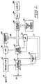
- a digital oscilloscope employs trigger holdoff circuit 10.
- An analog signal (INPUT) is applied via input terminal 12 to preamplifier 14, which suitably may be a conventional gain switching amplifier for amplifying and attenuating the input signal to a suitable level.
- preamplifier 14 which suitably may be a conventional gain switching amplifier for amplifying and attenuating the input signal to a suitable level.
- the preamplified signal is applied to analog-to-digital converter (ADC) 16, which converts the instantaneous value of the analog signal to n-bit parallel digital data at a rate determined by a sampling clock applied from time base control 18.
- ADC analog-to-digital converter
- the analog signal is also applied to trigger generator 20, which generates a trigger signal (TRIG) at a variable reference level determined by a trigger level potentiometer 22.
- the trigger signal is applied to time base control circuit 18, which also receives an acquisition start signal (ACQ START) from microprocessor 24 to enable time base control circuit 18.
- time base control circuit 18 After being enabled by the acquisition start signal, time base control circuit 18 sends a sampling clock signal to ADC 16 in response to initiation by the trigger pulse. Simultaneously, the sampling clock is counted by an address counter within time base control circuit 18.
- the address counter may be preset with a predetermind number to provide either pre-triggered or post-triggered operation.
- the n-bit digital data is clocked into acquisition memory 26 according to addresses designated via bus 28 by the address counter, as is well known in the art.
- time base control circuit 18 When the address counter reaches a count of the maximum address, time base control circuit 18 provides an acquisition complete signal (ACQ COMPLETE) to microprocessor 24, which in turn disables time base control circuit 18. Then the acquired waveform data is transferred from acquisition memory 26 to display memory 30.
- Microprocessor 24 reads the data from display memory 30 and processes it to measure amplitude and frequency, produce interpolated data etc. Display memory 30 is loaded with data representing a waveform by microprocessor 24 via bus 28. Now microprocessor 24 is free to start another waveform acquisition and provide an acquisition start signal again to time base control circuit 18.
- the stored data is clocked out of memory 30 under control of the display clock/ address counter 32, converted to an analog signal by digital-to-analog converter (DAC) 34 and displayed on the vertical axis of display device 36.
- DAC digital-to-analog converter
- the trigger signal (TRIG) produced by trigger generator 20 is also applied to trigger holdoff circuit 10 which produces holdoff pulses responsive to the leading edge of the trigger signals in this embodiment.
- the holdoff pulse signal is applied to a reset input terminal of trigger generator 20 to inhibit further triggers, indicated by the dotted trigger signal in Fig. 2, while the holdoff signal is in high state.
- the time interval of the high state is programmable by microprocessor 24 via bus 38 and trigger generator 20 may provide identical trigger pulses to time base control circuit 18 by adjusting the time interval of the holdoff pulse. Therefore, acquisition memory 24 starts data acquisition at the identical point on every acquisition cycle even if the processing time of microprocessor 24 is variable. Accordingly, repetitive waveforms displayed on display device 36 are stable.
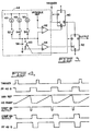
- Fig. 3 is a detailed schematic of one embodiment for generating a trigger holdoff signal in accordance with the present invention.
- the trigger signal is applied from trigger generator 20 to a clock input of D-type flip flop (FF) 40 which may suitably be a commercially available 74LS74 having S and D inputs connected to high levels.
- a Q output of D-type FF 40 is connected to the S input of D-type FF 42, which may be the same as D-type FF 40 having R and D inputs connected to high levels.
- Programmable timing circuit 44 includes current sources 46, 48 and 50, programmable switches 52, 54 and 56, timing capacitor 58, timing switch 60 and comparators 62 and 64. Switches 52, 54 and 56 are connected between each of current sources 46, 48 and 50 and timing capacitor 52.
- Timing switch 60 is connected across capacitor 58 and controlled by the Q output of D-type FF 40.
- the voltage ramp across capacitor 58 is made variable by programming switches 52, 54 and 56.
- the junction of the switches and capacitor 58 is connected to the inverted inputs of comparators 62 and 64 having non-inverting inputs respectively connected to a variable reference level and a ground potential, and having outputs respectively connected to the R input of D-type FF 40 and the clock input of D-type FF 42.
- Fig. 4 shows timing relation between the signals.
- the trigger signal applied to the clock input of D-type FF 40 causes the Q output thereof to go low, thereby opening switch 60.
- the programmed current from the current source group linearly charges capacitor 58 to produce a voltage ramp signal.
- the voltage ramp signal causes the output of comparator 64 to go low, thereby causing a Q output of D-type FF 42 (holdoff signal) to go high.
- Comparator 62 compares the voltage level of the ramp signal with the variable reference level and provides a high level output while the variable reference level is higher than the voltage level of the ramp signal.
- comparator 62 When the voltage ramp signal reaches the reference level, comparator 62 provides a low level pulse to the R input, thereby causing the Q output of D-type FF 40 to go high. The high level output from D-type FF 40 closes switch 60 to discharge capacitor 58 rapidly. When the voltage ramp goes to zero, the output of comparator 64 goes high, thereby causing the holdoff signal to go low. The holdoff signal is applied to trigger generator 20 to prevent it from generating triggers during the high level period of the holdoff signal. The next trigger causes the Q output of FF 40 to go high and the above- described operation will be repeated.
- timing circuit 44 could be implemented digitally using a programmable counter and variable clock, as well as a one shot multivibrator with variable capacitors and resistors.
Landscapes
- Physics & Mathematics (AREA)
- General Physics & Mathematics (AREA)
- Analogue/Digital Conversion (AREA)
- Information Transfer Systems (AREA)
Claims (5)
gekennzeichnet durch eine den Triggerimpuls aufnehmende Halteschaltung (10) zur Erzeugung eines Halteimpulses in Abhängigkeit davon zwecks Sperrung weiterer Triggerimpulse vom Triggergenerator (20) für eine vorgewählte Zeitdauer.
Applications Claiming Priority (2)
| Application Number | Priority Date | Filing Date | Title |
|---|---|---|---|
| US647004 | 1984-09-04 | ||
| US06/647,004 US4647862A (en) | 1984-09-04 | 1984-09-04 | Trigger holdoff system for a digital oscilloscope |
Publications (3)
| Publication Number | Publication Date |
|---|---|
| EP0174151A2 EP0174151A2 (de) | 1986-03-12 |
| EP0174151A3 EP0174151A3 (en) | 1987-05-20 |
| EP0174151B1 true EP0174151B1 (de) | 1990-07-11 |
Family
ID=24595323
Family Applications (1)
| Application Number | Title | Priority Date | Filing Date |
|---|---|---|---|
| EP85306074A Expired EP0174151B1 (de) | 1984-09-04 | 1985-08-27 | Verzögertes Triggersystem für ein Digital-Oszilloskop |
Country Status (4)
| Country | Link |
|---|---|
| US (1) | US4647862A (de) |
| EP (1) | EP0174151B1 (de) |
| JP (1) | JPH0692985B2 (de) |
| DE (1) | DE3578621D1 (de) |
Families Citing this family (21)
| Publication number | Priority date | Publication date | Assignee | Title |
|---|---|---|---|---|
| JPS6194136A (ja) * | 1984-10-15 | 1986-05-13 | Anritsu Corp | デイジタル信号処理装置 |
| DE3511592A1 (de) * | 1985-03-27 | 1986-10-02 | CREATEC Gesellschaft für Elektrotechnik mbH, 1000 Berlin | Signalverarbeitungsgeraet |
| US4771193A (en) * | 1985-12-27 | 1988-09-13 | Matsushita Electric Industrial Co., Ltd. | Synchronizing circuit |
| US4799165A (en) * | 1986-03-03 | 1989-01-17 | Tektronix, Inc. | Level detecting waveform sampling system |
| GB8616588D0 (en) * | 1986-07-08 | 1986-08-13 | Gould Electronics | Graphics display |
| JPS6341771U (de) * | 1986-09-05 | 1988-03-18 | ||
| JPH0424069U (de) * | 1990-06-20 | 1992-02-27 | ||
| US5223784A (en) * | 1991-06-01 | 1993-06-29 | Tektronix, Inc. | Method and circuit for triggering an electronic instrument only once during a period of a signal |
| US5268851A (en) * | 1991-10-21 | 1993-12-07 | Tektronix, Inc. | Detection of metastability in triggers |
| US5471159A (en) * | 1992-09-18 | 1995-11-28 | Tektronix, Inc. | Setup or hold violation triggering |
| US5412579A (en) * | 1993-04-05 | 1995-05-02 | Tektronix, Inc. | Slow display method for digital oscilloscope with fast acquisition system |
| US5446650A (en) * | 1993-10-12 | 1995-08-29 | Tektronix, Inc. | Logic signal extraction |
| US5754439A (en) * | 1995-12-26 | 1998-05-19 | Hewlett-Packard Co. | Method for reducing display locking in digital oscilloscopes or logic analyzers using inter-acquisition dithering techniques |
| US6275257B1 (en) * | 1998-10-16 | 2001-08-14 | Tektronix, Inc. | Holdoff by TV fields |
| US7068087B2 (en) * | 2004-02-24 | 2006-06-27 | Tektronix, Inc. | Method and apparatus for an improved timer circuit and pulse width detection |
| US7723976B2 (en) * | 2006-08-03 | 2010-05-25 | Tektronix, Inc. | Self-adjusting hold-off trigger |
| US8531176B2 (en) * | 2010-04-28 | 2013-09-10 | Teradyne, Inc. | Driving an electronic instrument |
| US8542005B2 (en) | 2010-04-28 | 2013-09-24 | Teradyne, Inc. | Connecting digital storage oscilloscopes |
| US8502522B2 (en) | 2010-04-28 | 2013-08-06 | Teradyne, Inc. | Multi-level triggering circuit |
| US9423843B2 (en) * | 2012-09-21 | 2016-08-23 | Atmel Corporation | Processor maintaining reset-state after reset signal is suspended |
| US12019098B2 (en) * | 2019-06-05 | 2024-06-25 | Tektronix, Inc. | Pattern acquisitions in equivalent time sampling systems |
Family Cites Families (10)
| Publication number | Priority date | Publication date | Assignee | Title |
|---|---|---|---|---|
| US3061788A (en) * | 1955-02-21 | 1962-10-30 | Tektronix Inc | Multivibrator hold-off circuit |
| DE2223672C2 (de) * | 1972-05-16 | 1974-03-14 | Hewlett-Packard Gmbh, 7030 Boeblingen | Triggerschaltung, insbesondere für Oszillografen |
| US4134149A (en) * | 1976-03-26 | 1979-01-09 | Norland Corporation | High sweep rate waveform display control for digital recording waveform devices |
| US4121164A (en) * | 1977-04-27 | 1978-10-17 | Tektronix, Inc. | Automatic trigger circuit |
| DE2912492A1 (de) * | 1979-03-29 | 1980-10-09 | Siemens Ag | Monolithisch integrierbarer rechteckimpulsgenerator |
| US4251754A (en) * | 1979-09-04 | 1981-02-17 | Tektronix, Inc. | Digital oscilloscope with reduced jitter due to sample uncertainty |
| US4404481A (en) * | 1980-10-20 | 1983-09-13 | Matsushita Electric Industrial Co., Ltd. | Capacitance to voltage conversion apparatus |
| US4495642A (en) * | 1982-02-26 | 1985-01-22 | Hewlett-Packard Company | Timing analyzer with combination transition and duration trigger |
| JPS5918666A (ja) * | 1982-07-22 | 1984-01-31 | Mitsubishi Electric Corp | 水冷機器の冷却装置 |
| US4555765A (en) | 1982-09-14 | 1985-11-26 | Analogic Corporation | Multi-mode oscilloscope trigger with compensating trigger delay |
-
1984
- 1984-09-04 US US06/647,004 patent/US4647862A/en not_active Expired - Lifetime
-
1985
- 1985-08-27 DE DE8585306074T patent/DE3578621D1/de not_active Expired - Lifetime
- 1985-08-27 EP EP85306074A patent/EP0174151B1/de not_active Expired
- 1985-09-03 JP JP60194707A patent/JPH0692985B2/ja not_active Expired - Lifetime
Also Published As
| Publication number | Publication date |
|---|---|
| EP0174151A2 (de) | 1986-03-12 |
| JPH0692985B2 (ja) | 1994-11-16 |
| DE3578621D1 (de) | 1990-08-16 |
| JPS6166167A (ja) | 1986-04-04 |
| US4647862A (en) | 1987-03-03 |
| EP0174151A3 (en) | 1987-05-20 |
Similar Documents
| Publication | Publication Date | Title |
|---|---|---|
| EP0174151B1 (de) | Verzögertes Triggersystem für ein Digital-Oszilloskop | |
| US4283713A (en) | Waveform acquisition circuit | |
| US5959479A (en) | Sampling timebase system | |
| US4271486A (en) | Waveform storage system | |
| US4982350A (en) | System for precise measurement of time intervals | |
| US4755951A (en) | Method and apparatus for digitizing a waveform | |
| US5115189A (en) | Anti-aliasing dithering method and apparatus for low frequency signal sampling | |
| US5180971A (en) | Method and apparatus for increasing throughput in random repetitive digitizing systems | |
| JPH0219653B2 (de) | ||
| US6121799A (en) | Interleaved digital peak detector | |
| US3893036A (en) | Precision function generator | |
| US4251754A (en) | Digital oscilloscope with reduced jitter due to sample uncertainty | |
| US4238727A (en) | Digitally programmable apparatus for generating a substantially linear ramp signal | |
| US4121164A (en) | Automatic trigger circuit | |
| US4704691A (en) | Trigger holdoff system for an oscilloscope | |
| CA1236579A (en) | Waveform memory circuit | |
| US4161029A (en) | Automatic transient response analyzer system | |
| EP0037207A2 (de) | Signalerzeugende Schaltungsanordnungen | |
| EP0174150B1 (de) | Verzögertes Triggersystem für ein Oszilloskop | |
| US4717883A (en) | Method and apparatus for reducing errors in a sampling system utilizing an error-sampled feedback loop | |
| US4771193A (en) | Synchronizing circuit | |
| US4190825A (en) | Logarithmic analog-to-digital converter | |
| CA1150842A (en) | Slide-back waveform analyzer | |
| EP0277702B1 (de) | Oszilloskop-Triggerkontrollschaltung | |
| US4823077A (en) | Channel-gain-vernier-tracking trigger hysteresis for an oscilloscope |
Legal Events
| Date | Code | Title | Description |
|---|---|---|---|
| PUAI | Public reference made under article 153(3) epc to a published international application that has entered the european phase |
Free format text: ORIGINAL CODE: 0009012 |
|
| AK | Designated contracting states |
Kind code of ref document: A2 Designated state(s): DE FR GB NL |
|
| PUAL | Search report despatched |
Free format text: ORIGINAL CODE: 0009013 |
|
| AK | Designated contracting states |
Kind code of ref document: A3 Designated state(s): DE FR GB NL |
|
| 17P | Request for examination filed |
Effective date: 19870611 |
|
| 17Q | First examination report despatched |
Effective date: 19890301 |
|
| GRAA | (expected) grant |
Free format text: ORIGINAL CODE: 0009210 |
|
| RAP1 | Party data changed (applicant data changed or rights of an application transferred) |
Owner name: TEKTRONIX, INC. |
|
| AK | Designated contracting states |
Kind code of ref document: B1 Designated state(s): DE FR GB NL |
|
| ET | Fr: translation filed | ||
| RAP2 | Party data changed (patent owner data changed or rights of a patent transferred) |
Owner name: TEKTRONIX, INC. |
|
| REF | Corresponds to: |
Ref document number: 3578621 Country of ref document: DE Date of ref document: 19900816 |
|
| PLBE | No opposition filed within time limit |
Free format text: ORIGINAL CODE: 0009261 |
|
| STAA | Information on the status of an ep patent application or granted ep patent |
Free format text: STATUS: NO OPPOSITION FILED WITHIN TIME LIMIT |
|
| 26N | No opposition filed | ||
| PGFP | Annual fee paid to national office [announced via postgrant information from national office to epo] |
Ref country code: NL Payment date: 19960723 Year of fee payment: 12 |
|
| PG25 | Lapsed in a contracting state [announced via postgrant information from national office to epo] |
Ref country code: NL Free format text: LAPSE BECAUSE OF NON-PAYMENT OF DUE FEES Effective date: 19980301 |
|
| NLV4 | Nl: lapsed or anulled due to non-payment of the annual fee |
Effective date: 19980301 |
|
| REG | Reference to a national code |
Ref country code: GB Ref legal event code: IF02 |
|
| PGFP | Annual fee paid to national office [announced via postgrant information from national office to epo] |
Ref country code: FR Payment date: 20040708 Year of fee payment: 20 |
|
| PGFP | Annual fee paid to national office [announced via postgrant information from national office to epo] |
Ref country code: GB Payment date: 20040712 Year of fee payment: 20 |
|
| PGFP | Annual fee paid to national office [announced via postgrant information from national office to epo] |
Ref country code: DE Payment date: 20040716 Year of fee payment: 20 |
|
| PG25 | Lapsed in a contracting state [announced via postgrant information from national office to epo] |
Ref country code: GB Free format text: LAPSE BECAUSE OF EXPIRATION OF PROTECTION Effective date: 20050826 |
|
| REG | Reference to a national code |
Ref country code: GB Ref legal event code: PE20 |