EP0171027B1 - Optical transmitter - Google Patents
Optical transmitter Download PDFInfo
- Publication number
- EP0171027B1 EP0171027B1 EP85109595A EP85109595A EP0171027B1 EP 0171027 B1 EP0171027 B1 EP 0171027B1 EP 85109595 A EP85109595 A EP 85109595A EP 85109595 A EP85109595 A EP 85109595A EP 0171027 B1 EP0171027 B1 EP 0171027B1
- Authority
- EP
- European Patent Office
- Prior art keywords
- dfb
- current
- lasing
- bistable
- layer
- Prior art date
- Legal status (The legal status is an assumption and is not a legal conclusion. Google has not performed a legal analysis and makes no representation as to the accuracy of the status listed.)
- Expired - Lifetime
Links
Images

Classifications
-
- H—ELECTRICITY
- H01—ELECTRIC ELEMENTS
- H01S—DEVICES USING THE PROCESS OF LIGHT AMPLIFICATION BY STIMULATED EMISSION OF RADIATION [LASER] TO AMPLIFY OR GENERATE LIGHT; DEVICES USING STIMULATED EMISSION OF ELECTROMAGNETIC RADIATION IN WAVE RANGES OTHER THAN OPTICAL
- H01S5/00—Semiconductor lasers
- H01S5/06—Arrangements for controlling the laser output parameters, e.g. by operating on the active medium
- H01S5/0601—Arrangements for controlling the laser output parameters, e.g. by operating on the active medium comprising an absorbing region
-
- H—ELECTRICITY
- H01—ELECTRIC ELEMENTS
- H01S—DEVICES USING THE PROCESS OF LIGHT AMPLIFICATION BY STIMULATED EMISSION OF RADIATION [LASER] TO AMPLIFY OR GENERATE LIGHT; DEVICES USING STIMULATED EMISSION OF ELECTROMAGNETIC RADIATION IN WAVE RANGES OTHER THAN OPTICAL
- H01S5/00—Semiconductor lasers
- H01S5/10—Construction or shape of the optical resonator, e.g. extended or external cavity, coupled cavities, bent-guide, varying width, thickness or composition of the active region
- H01S5/12—Construction or shape of the optical resonator, e.g. extended or external cavity, coupled cavities, bent-guide, varying width, thickness or composition of the active region the resonator having a periodic structure, e.g. in distributed feedback [DFB] lasers
-
- G—PHYSICS
- G02—OPTICS
- G02F—OPTICAL DEVICES OR ARRANGEMENTS FOR THE CONTROL OF LIGHT BY MODIFICATION OF THE OPTICAL PROPERTIES OF THE MEDIA OF THE ELEMENTS INVOLVED THEREIN; NON-LINEAR OPTICS; FREQUENCY-CHANGING OF LIGHT; OPTICAL LOGIC ELEMENTS; OPTICAL ANALOGUE/DIGITAL CONVERTERS
- G02F3/00—Optical logic elements; Optical bistable devices
- G02F3/02—Optical bistable devices
- G02F3/026—Optical bistable devices based on laser effects
-
- H—ELECTRICITY
- H01—ELECTRIC ELEMENTS
- H01S—DEVICES USING THE PROCESS OF LIGHT AMPLIFICATION BY STIMULATED EMISSION OF RADIATION [LASER] TO AMPLIFY OR GENERATE LIGHT; DEVICES USING STIMULATED EMISSION OF ELECTROMAGNETIC RADIATION IN WAVE RANGES OTHER THAN OPTICAL
- H01S5/00—Semiconductor lasers
- H01S5/06—Arrangements for controlling the laser output parameters, e.g. by operating on the active medium
- H01S5/0601—Arrangements for controlling the laser output parameters, e.g. by operating on the active medium comprising an absorbing region
- H01S5/0602—Arrangements for controlling the laser output parameters, e.g. by operating on the active medium comprising an absorbing region which is an umpumped part of the active layer
-
- H—ELECTRICITY
- H01—ELECTRIC ELEMENTS
- H01S—DEVICES USING THE PROCESS OF LIGHT AMPLIFICATION BY STIMULATED EMISSION OF RADIATION [LASER] TO AMPLIFY OR GENERATE LIGHT; DEVICES USING STIMULATED EMISSION OF ELECTROMAGNETIC RADIATION IN WAVE RANGES OTHER THAN OPTICAL
- H01S5/00—Semiconductor lasers
- H01S5/06—Arrangements for controlling the laser output parameters, e.g. by operating on the active medium
- H01S5/062—Arrangements for controlling the laser output parameters, e.g. by operating on the active medium by varying the potential of the electrodes
- H01S5/06209—Arrangements for controlling the laser output parameters, e.g. by operating on the active medium by varying the potential of the electrodes in single-section lasers
- H01S5/06216—Pulse modulation or generation
-
- H—ELECTRICITY
- H01—ELECTRIC ELEMENTS
- H01S—DEVICES USING THE PROCESS OF LIGHT AMPLIFICATION BY STIMULATED EMISSION OF RADIATION [LASER] TO AMPLIFY OR GENERATE LIGHT; DEVICES USING STIMULATED EMISSION OF ELECTROMAGNETIC RADIATION IN WAVE RANGES OTHER THAN OPTICAL
- H01S5/00—Semiconductor lasers
- H01S5/20—Structure or shape of the semiconductor body to guide the optical wave ; Confining structures perpendicular to the optical axis, e.g. index or gain guiding, stripe geometry, broad area lasers, gain tailoring, transverse or lateral reflectors, special cladding structures, MQW barrier reflection layers
- H01S5/22—Structure or shape of the semiconductor body to guide the optical wave ; Confining structures perpendicular to the optical axis, e.g. index or gain guiding, stripe geometry, broad area lasers, gain tailoring, transverse or lateral reflectors, special cladding structures, MQW barrier reflection layers having a ridge or stripe structure
- H01S5/227—Buried mesa structure ; Striped active layer
- H01S5/2275—Buried mesa structure ; Striped active layer mesa created by etching
Definitions
- the present invention relates to an optical transmitter for optical fiber communications.
- DFB LDs distributed feedback semiconductor lasers
- APDs high sensitivity light receiving elements
- optical fiber communications over a distance of more than 100 km has recently been brought to a practicable stage. Studies are presently under way for further increasing the transmission range or the transmission rate.
- the carrier density of an active layer in the DFB LD is modulated and, therefore, the lasing wavelength is necessarily modulated ("wavelength chirping" as generally referred to), undesirably allowing the spectrum line width to expand to about 1 - 2 ⁇ .
- wavelength chirping as generally referred to
- the transmissible distance is limited by wavelength dispersion rather than by transmission loss.
- an optical transmitter including a bistable distributed feedback semiconductor laser having hysteresis which includes a first lasing threshold value associated with a case wherein an injection current is increased and a second lasing threshold value associated with a case wherein the injection current is decreased, a bias circuit applying a bias current lower than the second lasing threshold value to the semiconductor laser, and a drive circuit applying to the semiconductor laser a current pulse having a peak which is higher than the first lasing threshold value when the current pulse is superimposed on the bias current.
- bistable DFB LD which constitutes an essential element of the present invention. Even with a DFB LD, a bistable mode operation is attainable by defining a non-injection region where no current is injected, as taught by Akiba et al in IEEE Journal of Quantum Electronics. Vol. QE-19, No. 6, page 1053, issued 1983.
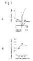
- the light output of the above-mentioned type of DFB LD showed a hysteresis characteristics responsive to injection current; the lasing threshold current I ON'th at the time of rise measured 60 mA and the lasing threshold current I OFF,th at the time of fall, 50 mA.
- the previously mentioned paper presented by Akiba et al teaches such a hysteresis characteristic.
- a rectangular pulse current was applied to a bistable DFB LD having the above-described characteristic to evaluate its response.
- a dc bias current I b was set at 48 mA which was lower than I OFF,th and pulses having a peak value of 15 mA and a width of 5 ns were applied to the DEB LD.
- the resulting light output showed significant relaxation oscillation in its waveform at the time of rise.
- a semi-conductor laser under such significant relaxation oscillation shows a significant change in lasing frequency because the carrier density of its active layer is greatly modulated.
- the tested bistable DFB LD has a lasing spectrum line width of about 600 MHz in terms of half width as shown in FIG. 4B and, thus, the amount of fluctuation of lasing frequency is small.
- the reason is that, as shwon in FIG. 3B, when the DFB LD is caused to lase by increased injection currents, the fluctuation of the oscillation frequency remains insignificant at those current values with no regard to the fluctuation of the carrier density of the active layer and, hence, the lasing frequency little fluctuates despite substantial fluctuation of light output, i.e. substantial intensity modulation of light.
- bistable DFB LD Such a characteristic of a bistable DFB LD is applicable to optical fiber communications.
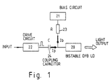
- an optical transmitter embodying the present invention is shown in a block diagram.
- the optical transmitter comprises a bias circuit 21 and a drive circuit 22 which in cooperation serve to activate a bistable DFB LD 20, and a coupling resistor 23 and a coupling capacitor 24.
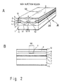
- the bistable DFB LD has a mesa stripe which includes an active layer 3, a waveguide layer 4 conjugate with the active layer 3 and provided with corrugation having a predetermined period, and a cladding layer 5 which holds the waveguide layer 4 between it and the active layer 3.
- the DFB LD includes an n-InP confining layer 7 provided on an intermediate portion of the mesa stripe, and a P-InP burying layer 8 and a cap layer 9.
- a voltage is applied across a positive electrode 10 and a negative electrode 11 to inject current into the active layer 3.
- the particular part of the active layer 3 located below the confining layer 7 defines a non-injection region where current injection does not occur, so that the light output shows a bistable characteristic.
- the procedure for manufacturing the DFB LD 20 will be described later in detail.
- the coupling resistor 23 had a resistance value of 50 ⁇ and the coupling capacitor 24 a capacitance of 1 ⁇ F in order to suppress leakage of electricity between the bias circuit 21 and the drive circuit 22.
- An output signal of a 450 MHz pseudo-random pulse generator was used as an input signal for operating the light transmitter.
- the evaluation showed that the bistable DFB LD 20 generates optical signal pulses which follow the input signal, and that the optical pulses are each 7 mW high.
- the spectrum of the modulated light signal was found by evaluation to be similar to the spectrum shown in FIG. 4B and, in addition, optical signals modulated by random pulses also had a lasing spectrum line width as narrow as about 600 MHz.
- Transmission tests were conducted by introducing optical signals provided by the optical transmitter of the present invention into single mode fibers having a core diameter of 10 ⁇ m through an optical lens arrangement and with a coupling loss of 2 dB.
- a receiver used for the tests was implemented with a Ge-APD having a light receiving diameter of 80 ⁇ m.
- the received power level of the receiver was -42 dBm for a bit error rate of 10 ⁇ 10 S ⁇ 1.
- optical fibers which show an average transmission loss of 0.25 dB/km inclusive of splice losses of the optical fibers at the wavelength in the 1.55 ⁇ m band was used, the transmitter successfully transmitted signals over a distance of 160 km with a margin of 2 dBm.
- the spectrum line width measured about 3 GHz with the result that the transmissible range was limited to 100 km due to the influence of wavelength dispersion.
- the DFB LD 20 comprises a (001) n-InP substrate 1 on which are sequentially grown an n-InP buffer layer 2 (Sn-doped, carrier density of 5 x 1017 cm ⁇ 3, thickness of 3 ⁇ m), a non-doped InGaAsP active layer 3 (1.3 ⁇ m composition in terms of emission wavelength, thickness of 0.1 ⁇ m), and p-InGaAsP guide layer 4 (1.1 ⁇ m composition in terms of emission wavelength, Zn-doped, carrier density of 7 x 1018 cm ⁇ 3, thickness of 0.2 ⁇ m).
- n-InP buffer layer 2 Sn-doped, carrier density of 5 x 1017 cm ⁇ 3, thickness of 3 ⁇ m
- a non-doped InGaAsP active layer 3 1.3 ⁇ m composition in terms of emission wavelength, thickness of 0.1 ⁇ m
- p-InGaAsP guide layer 4 1.1 ⁇ m composition in terms of emission wavelength, Zn-doped, carrier density of
- the p-InGaAsP guide layer 4 is provided with a diffraction grating 200 having a period of 200 nm and a depth of 100 nm.
- a p-InP cladding layer 5 (Zn-doped, carrier density of 1 x 1018 cm ⁇ 3, and thickness of 1 ⁇ m) is deposited on the surface of the wafer which has been provided with the diffraction grating 200.
- a p-InP blocking layer 6 Zn-doped, carrier density of 1 x 1018 cm ⁇ 3, 0.5 ⁇ m thick in flat portion
- an n-InP confining layer 7 Ti-doped, carrier density of 3 x 1018 cm ⁇ 3, 0.5 ⁇ m thick in flat portion
- a p-InP burying layer 8 Zn-doped, carrier density of 1 x 1018 cm ⁇ 3, 1.5 ⁇ m thick in flat portion
- a p-InGaAsP cap layer 9 1.2 ⁇ m thick composition in terms of emission wavelength, Z-doped, carrier density of 1 x 1019 cm ⁇ 3, about 1 ⁇ m thick in a flat portion
- the n-InP confining layer 7 is laminated exclusively on that part of the mesa stripe 50 which lies in the non-injection region 100. To grown the confining layer 7 only in the limited region 100, the two channels 51 and 52 may each be narrowed in the specific region 100. In the non-injection region 100, the confining layer 7 serves to prevent a current from being injected into the InGaAsP active layer 3 which is located beneath the confining layer 7.
- bistable DFB LD While only basic structural elements are shown in the embodiment of Fig. 1, it will be noted that a temperature control unit for controlling the operation temperature of the bistable DFB LD to a predetermined value, a light isolator for reducing the influence of light returning to the DFB LD, and others may be incorporated, if desired. It Should be born in mind that the bistable DFB LD structure and current values shown and described are merely typical examples and not restrictive in any way, that is, the present invention is applicable to any kind of DFB LDs.
- the present invention provides an optical transmitter which offers a remarkable improvement in transmissible distance over prior art transmitters.
- This advantage is derived from the fact that since the transmitter of the present invention is capable of generating signal pulses having a narrow lasing spectrum line width, it is free from the limitation due to wavelength dispersion of optical fibers when applied to an optical fiber communications system.
Description
- The present invention relates to an optical transmitter for optical fiber communications.
- With the advent of low-loss optical fibers, single-mode semiconductor lasers such as distributed feedback semiconductor lasers (hereinafter referred to as DFB LDs for brevity), high sensitivity light receiving elements such as germanium or InGaAs avalanche photodiodes (hereinafter referred to as APDs for brevity), and the like, optical fiber communications over a distance of more than 100 km has recently been brought to a practicable stage. Studies are presently under way for further increasing the transmission range or the transmission rate.
- One of major obstructions to longer range and higher rate lightwave communications is the wavelength dispersion of optical fibers. Specifically, while in the wavelength range of 1.5 - 1.6 µm the transmission loss of optical fibers is minimal and long-distance transmission is hopeful, the wavelength dispersion due mainly to material dispersion amounts to about -2 ps/km/Å (1Å = 0.1 nm)in that specific wavelength range. Hence, in order that transmission may be effected over a distance of the order of 100 km with a modulation rate of 2 Gb/s, a light source which naturally is operable in a single longitudinal mode is essential and, yet, the spread of its spectrum width has to be restricted to about 0.8 Å. However, where a prior art DFB LD is directly modulated at a high rate, the carrier density of an active layer in the DFB LD is modulated and, therefore, the lasing wavelength is necessarily modulated ("wavelength chirping" as generally referred to), undesirably allowing the spectrum line width to expand to about 1 - 2 Å. As such, where high-speed transmission is desired in the wavelength band of 1.5 µm, the transmissible distance is limited by wavelength dispersion rather than by transmission loss.
- It is therefore an object of the present invention to provide an optical transmitter for optical fiber communications which allows a minimum of wavelength chirping to occur even during high-speed direct modulation.
- In accordance with the present invention, there is provided an optical transmitter including a bistable distributed feedback semiconductor laser having hysteresis which includes a first lasing threshold value associated with a case wherein an injection current is increased and a second lasing threshold value associated with a case wherein the injection current is decreased, a bias circuit applying a bias current lower than the second lasing threshold value to the semiconductor laser, and a drive circuit applying to the semiconductor laser a current pulse having a peak which is higher than the first lasing threshold value when the current pulse is superimposed on the bias current.
-
- FIG. 1 is a block diagram of an optical transmitter embodying the present invention which partly shows specific circuit elements;
- FIG. 2A is a perspective view of a bistable DFB LD applicable to the embodiment of the present invention;
- FIG. 2B is a section along line BADC of FIG. 2A;
- FIGS. 3A and 3B are plots showing respectively an L-I characteristic of a bistable DFB LD and shifts of lasing frequency; and
- FIGS. 4A and 4B are charts showing respectively a current waveform and a modulated waveform of light output, and shifts of lasing frequency during modulation.
- Before entering into detailed description of the present invention, the characteristics of a bistable DFB LD which constitutes an essential element of the present invention will be outlined. Even with a DFB LD, a bistable mode operation is attainable by defining a non-injection region where no current is injected, as taught by Akiba et al in IEEE Journal of Quantum Electronics. Vol. QE-19, No. 6, page 1053, issued 1983. A bistable DFB LD shown in FIGS. 2A and 2B of the drawings was manufactured for test by providing a
non-injection region 100 in a part of a double-channel planer buried DFB LD which had been reported by Yamaguchi et al at the 1984 National Convention (Record) of the Institute of Electronics and Communication Engineers of Japan, Paper No. 1026. - As shown in Fig. 3A, the light output of the above-mentioned type of DFB LD showed a hysteresis characteristics responsive to injection current; the lasing threshold current ION'th at the time of rise measured 60 mA and the lasing threshold current IOFF,th at the time of fall, 50 mA. The previously mentioned paper presented by Akiba et al teaches such a hysteresis characteristic. By measuring a lasing spectrum in relation to injection current, it was proved that a single mode operation with a lasing wavelength of 1,550 µm occurs in an injection current range of the order of 50 - 100 mA. However, more precise measurement of the lasing wavelength showed that the frequency slightly shifts depending upon the injection current, as plotted in Fig. 3B. Even in an ordinary DFB LD the lasing frequency shifts responsive to an increase of injection current due to the influence of a change in the carrier density of the active layer as well as an increase in the temperature of the same layer, but a bistable DFB LD showed behavior different from that of the ordinary DFB LD. Specifically, it was found to have a peak at a current which is slightly about ION,th and little change the lasing frequency despite current changes in the vicinity of ION,th. The shift of the lasing frequency responsive to currents in the vicinity of IOFF,th is 0.6 - 0.8 GHz/mA which is greater than the ordinary DFB LD which lacks a non-injection region.
- A rectangular pulse current was applied to a bistable DFB LD having the above-described characteristic to evaluate its response. Specifically, as shown in Fig. 4A, a dc bias current Ib was set at 48 mA which was lower than IOFF,th and pulses having a peak value of 15 mA and a width of 5 ns were applied to the DEB LD. The resulting light output showed significant relaxation oscillation in its waveform at the time of rise. Generally, a semi-conductor laser under such significant relaxation oscillation shows a significant change in lasing frequency because the carrier density of its active layer is greatly modulated. However, it was found that the tested bistable DFB LD has a lasing spectrum line width of about 600 MHz in terms of half width as shown in FIG. 4B and, thus, the amount of fluctuation of lasing frequency is small. The reason is that, as shwon in FIG. 3B, when the DFB LD is caused to lase by increased injection currents, the fluctuation of the oscillation frequency remains insignificant at those current values with no regard to the fluctuation of the carrier density of the active layer and, hence, the lasing frequency little fluctuates despite substantial fluctuation of light output, i.e. substantial intensity modulation of light.
- The phenomenon stated above is the first revelation in conjunction with a bistable DFB LD. Such a characteristic of a bistable DFB LD is applicable to optical fiber communications.
- Referring to FIG. 1 of the drawings, an optical transmitter embodying the present invention is shown in a block diagram. The optical transmitter comprises a
bias circuit 21 and adrive circuit 22 which in cooperation serve to activate a bistable DFB LD 20, and acoupling resistor 23 and acoupling capacitor 24. As shown in detail in FIGS. 2A and 2B, the bistable DFB LD has a mesa stripe which includes an active layer 3, a waveguide layer 4 conjugate with the active layer 3 and provided with corrugation having a predetermined period, and a cladding layer 5 which holds the waveguide layer 4 between it and the active layer 3. In addition to the layers 3, 4 and 5, the DFB LD includes an n-InP confining layer 7 provided on an intermediate portion of the mesa stripe, and a P-InP burying layer 8 and acap layer 9. A voltage is applied across apositive electrode 10 and anegative electrode 11 to inject current into the active layer 3. The particular part of the active layer 3 located below the confining layer 7 defines a non-injection region where current injection does not occur, so that the light output shows a bistable characteristic. The procedure for manufacturing the DFB LD 20 will be described later in detail. - To evaluate the characteristics of the light transmitter shown in Fig. 1, a bias current Ib of 48 mA which is lower than the threshold current IOFF,th = 50 mA for the biastable DFB LD to turn off was applied to the DFB
LD 20. Applied to the DFBLD 20 from thedrive circuit 22 was a pulse current Ip having a peak value of 15 mA, which is higher than the threshold current ION,th = 60 mA for the DFBLD 20 to turn on, when superposed on the bias current Ib responsive to an input signal. Thecoupling resistor 23 had a resistance value of 50 Ω and the coupling capacitor 24 a capacitance of 1 µF in order to suppress leakage of electricity between thebias circuit 21 and thedrive circuit 22. An output signal of a 450 MHz pseudo-random pulse generator was used as an input signal for operating the light transmitter. The evaluation showed that the bistable DFBLD 20 generates optical signal pulses which follow the input signal, and that the optical pulses are each 7 mW high. The spectrum of the modulated light signal was found by evaluation to be similar to the spectrum shown in FIG. 4B and, in addition, optical signals modulated by random pulses also had a lasing spectrum line width as narrow as about 600 MHz. - Transmission tests were conducted by introducing optical signals provided by the optical transmitter of the present invention into single mode fibers having a core diameter of 10 µm through an optical lens arrangement and with a coupling loss of 2 dB. A receiver used for the tests was implemented with a Ge-APD having a light receiving diameter of 80 µm. The received power level of the receiver was -42 dBm for a bit error rate of 10⁻¹⁰ S⁻¹. When optical fibers which show an average transmission loss of 0.25 dB/km inclusive of splice losses of the optical fibers at the wavelength in the 1.55 µm band was used, the transmitter successfully transmitted signals over a distance of 160 km with a margin of 2 dBm. It was found that this distance is the result of limitation due to losses and not to the dispersion of the optical fibers, and that the lasing spectrum line width of signal light is restricted to a sufficiently small value. Such implies that modulating the
bistable DFB LD 20 in such a manner as to traverse the hysteresis region is sufficiently effective. In this connection, when the bias current Ib was increased so as to modulate thebistable DFB LD 20 in such a manner as not to traverse the hysteresis region, that is, when the bias current Ib was controlled to a value between ION,th and IOFF,th and the pulse current was superposed on such a bias current Ib for modulation, the spectrum line width measured about 3 GHz with the result that the transmissible range was limited to 100 km due to the influence of wavelength dispersion. - Now, a reference will be made to FIGS. 2A and 2B for explaining the method of manufacturing the
DFB LD 20. TheDFB LD 20 comprises a (001) n-InP substrate 1 on which are sequentially grown an n-InP buffer layer 2 (Sn-doped, carrier density of 5 x 10¹⁷ cm⁻³, thickness of 3 µm), a non-doped InGaAsP active layer 3 (1.3 µm composition in terms of emission wavelength, thickness of 0.1 µm), and p-InGaAsP guide layer 4 (1.1 µm composition in terms of emission wavelength, Zn-doped, carrier density of 7 x 10¹⁸ cm⁻³, thickness of 0.2 µm). The p-InGaAsP guide layer 4 is provided with adiffraction grating 200 having a period of 200 nm and a depth of 100 nm. A p-InP cladding layer 5 (Zn-doped, carrier density of 1 x 10¹⁸ cm⁻³, and thickness of 1 µm) is deposited on the surface of the wafer which has been provided with thediffraction grating 200. After two parallel channels orgrooves mesa stripe 50 which is 1 - 2 µm thick, there are sequentially grown a p-InP blocking layer 6 (Zn-doped, carrier density of 1 x 10¹⁸ cm⁻³, 0.5 µm thick in flat portion), an n-InP confining layer 7 (Te-doped, carrier density of 3 x 10¹⁸ cm⁻³, 0.5 µm thick in flat portion), a p-InP burying layer 8 (Zn-doped, carrier density of 1 x 10¹⁸ cm⁻³, 1.5 µm thick in flat portion), and a p-InGaAsP cap layer 9 (1.2 µm thick composition in terms of emission wavelength, Z-doped, carrier density of 1 x 10¹⁹ cm⁻³, about 1 µm thick in a flat portion), thereby completing a double-channel planer buried structure. Some of the layers mentioned have already been outlined in relation to the specific construction of the transmitter of the present invention. The n-InP confining layer 7 is laminated exclusively on that part of themesa stripe 50 which lies in thenon-injection region 100. To grown the confining layer 7 only in thelimited region 100, the twochannels specific region 100. In thenon-injection region 100, the confining layer 7 serves to prevent a current from being injected into the InGaAsP active layer 3 which is located beneath the confining layer 7. - While only basic structural elements are shown in the embodiment of Fig. 1, it will be noted that a temperature control unit for controlling the operation temperature of the bistable DFB LD to a predetermined value, a light isolator for reducing the influence of light returning to the DFB LD, and others may be incorporated, if desired. It Should be born in mind that the bistable DFB LD structure and current values shown and described are merely typical examples and not restrictive in any way, that is, the present invention is applicable to any kind of DFB LDs.
- In summary, it will be seen that the present invention provides an optical transmitter which offers a remarkable improvement in transmissible distance over prior art transmitters. This advantage is derived from the fact that since the transmitter of the present invention is capable of generating signal pulses having a narrow lasing spectrum line width, it is free from the limitation due to wavelength dispersion of optical fibers when applied to an optical fiber communications system.
Claims (1)
- An optical transmitter comprising:
a bistable distributed feedback semiconductor laser having a hysteresis characteristic which has a first lasing threshold value for said laser to start lasing when an injection current is increased and a second lasing threshold value for the laser to stop lasing when the injection current is decreased;
biasing means applying a bias current lower than said second lasing threshold value to said semiconductor laser; and
driving means applying to the semiconductor laser a current pulse having a peak which is higher than said first lasing threshold value when the current pulse is superimposed on said bias current.
Applications Claiming Priority (2)
| Application Number | Priority Date | Filing Date | Title |
|---|---|---|---|
| JP15982384A JPS6139643A (en) | 1984-07-30 | 1984-07-30 | Light transmitting device |
| JP159823/84 | 1984-07-30 |
Publications (3)
| Publication Number | Publication Date |
|---|---|
| EP0171027A2 EP0171027A2 (en) | 1986-02-12 |
| EP0171027A3 EP0171027A3 (en) | 1988-12-21 |
| EP0171027B1 true EP0171027B1 (en) | 1991-12-04 |
Family
ID=15702027
Family Applications (1)
| Application Number | Title | Priority Date | Filing Date |
|---|---|---|---|
| EP85109595A Expired - Lifetime EP0171027B1 (en) | 1984-07-30 | 1985-07-30 | Optical transmitter |
Country Status (4)
| Country | Link |
|---|---|
| US (1) | US4947458A (en) |
| EP (1) | EP0171027B1 (en) |
| JP (1) | JPS6139643A (en) |
| DE (1) | DE3584801D1 (en) |
Families Citing this family (3)
| Publication number | Priority date | Publication date | Assignee | Title |
|---|---|---|---|---|
| JPS61201222A (en) * | 1985-03-04 | 1986-09-05 | Hitachi Ltd | Light pulse amplifying and shaping device |
| US20010048799A1 (en) * | 1998-05-21 | 2001-12-06 | F. David King | Optical communication system |
| US6944404B2 (en) * | 2000-12-11 | 2005-09-13 | Harris Corporation | Network transceiver for extending the bandwidth of optical fiber-based network infrastructure |
Family Cites Families (11)
| Publication number | Priority date | Publication date | Assignee | Title |
|---|---|---|---|---|
| US3680001A (en) * | 1971-05-13 | 1972-07-25 | Bell Telephone Labor Inc | Dynamic am control of the transverse modes of a self-pulsing semiconductor laser |
| JPS5967677A (en) * | 1982-07-01 | 1984-04-17 | Semiconductor Res Found | Photo integrated circuit |
| JPS5992587A (en) * | 1982-11-18 | 1984-05-28 | Nec Corp | Photo amplification circuit |
| US4608682A (en) * | 1982-11-29 | 1986-08-26 | Nec Corporation | Optical time-division switching system employing optical bistable devices |
| JPS59117285A (en) * | 1982-12-24 | 1984-07-06 | Nec Corp | Optical amplifier circuit |
| JPS59182637A (en) * | 1983-03-31 | 1984-10-17 | Matsushita Electric Ind Co Ltd | Optical transmitter of video signal |
| US4558465A (en) * | 1983-09-19 | 1985-12-10 | Rca Corporation | Switched bias scheme for high speed laser transmitter |
| JPS6079786A (en) * | 1983-10-06 | 1985-05-07 | Nec Corp | Bistable laser |
| JPS6079788A (en) * | 1983-10-06 | 1985-05-07 | Nec Corp | Optical bistable element |
| JPS60102789A (en) * | 1983-11-09 | 1985-06-06 | Kokusai Denshin Denwa Co Ltd <Kdd> | Distributed feedback semiconductor laser |
| CA1210070A (en) * | 1984-10-26 | 1986-08-19 | Northern Telecom Limited | Laser transmitter |
-
1984
- 1984-07-30 JP JP15982384A patent/JPS6139643A/en active Pending
-
1985
- 1985-07-30 DE DE8585109595T patent/DE3584801D1/en not_active Expired - Fee Related
- 1985-07-30 US US06/760,560 patent/US4947458A/en not_active Expired - Fee Related
- 1985-07-30 EP EP85109595A patent/EP0171027B1/en not_active Expired - Lifetime
Also Published As
| Publication number | Publication date |
|---|---|
| US4947458A (en) | 1990-08-07 |
| JPS6139643A (en) | 1986-02-25 |
| DE3584801D1 (en) | 1992-01-16 |
| EP0171027A2 (en) | 1986-02-12 |
| EP0171027A3 (en) | 1988-12-21 |
Similar Documents
| Publication | Publication Date | Title |
|---|---|---|
| US5590145A (en) | Light-emitting apparatus capable of selecting polarization direction, optical communication system, and polarization modulation control method | |
| Koyama et al. | 1.5-1.6 µm GaInAsP/InP dynamic-single-mode (DSM) lasers with distributed Bragg reflector | |
| US5764670A (en) | Semiconductor laser apparatus requiring no external modulator, method of driving semiconductor laser device, and optical communication system using the semiconductor laser apparatus | |
| US5878066A (en) | Optical semiconductor apparatus driving method therefor light source apparatus and optical communication system using the same | |
| JPH06216467A (en) | Semiconductor light-dispersion compensator | |
| EP0718937B1 (en) | Method of driving a polarization mode selective semiconductor laser with a wide modulation band, and an optical communication system | |
| JPH06103778B2 (en) | Optical device including semiconductor distributed feedback laser and method of driving the same | |
| Suzuki et al. | lambda/4-shifted DFB laser/electroabsorption modulator integrated light source for multigigabit transmission | |
| US4947400A (en) | Laser-photodetector assemblage | |
| EP0171027B1 (en) | Optical transmitter | |
| Iwashita et al. | Mode partition noise characteristics in high-speed modulated laser diodes | |
| EP0189252A2 (en) | Semiconductor laser direct frequency modulation system | |
| Yamaguchi et al. | Requirements for modulator-integrated DFB LD's for penalty-free 2.5-Gb/s transmission | |
| JPH08248364A (en) | Light intensity modulation element and semiconductor laser with light intensity modulation element | |
| Tsang et al. | The heteroepitaxial ridge-overgrown distributed feedback laser | |
| Yasaka et al. | Finely tunable wavelength conversion of high bit-rate signals by using a superstructure-grating distributed Bragg reflector laser | |
| Ishizaka et al. | Modulator integrated DFB lasers with more than 600-km transmission capability at 2.5 Gb/s | |
| Inoue | Optical filtering to reduce chirping influence in LD wavelength conversion | |
| Ishizaka et al. | The transmission capability of a 10-Gb/s electroabsorption modulator integrated DFB laser using the offset bias chirp reduction technique | |
| JP2001290114A (en) | Optical transmitting module | |
| JP7147611B2 (en) | High power directly modulated laser | |
| JPS6281086A (en) | Optical transmitter | |
| JP3450573B2 (en) | Semiconductor laser device, driving method thereof, and optical communication system using the same | |
| JPH0550875B2 (en) | ||
| JP2596186B2 (en) | Integrated semiconductor optical modulator |
Legal Events
| Date | Code | Title | Description |
|---|---|---|---|
| PUAI | Public reference made under article 153(3) epc to a published international application that has entered the european phase |
Free format text: ORIGINAL CODE: 0009012 |
|
| 17P | Request for examination filed |
Effective date: 19850730 |
|
| AK | Designated contracting states |
Designated state(s): DE FR GB |
|
| PUAL | Search report despatched |
Free format text: ORIGINAL CODE: 0009013 |
|
| AK | Designated contracting states |
Kind code of ref document: A3 Designated state(s): DE FR GB |
|
| 17Q | First examination report despatched |
Effective date: 19910308 |
|
| GRAA | (expected) grant |
Free format text: ORIGINAL CODE: 0009210 |
|
| AK | Designated contracting states |
Kind code of ref document: B1 Designated state(s): DE FR GB |
|
| REF | Corresponds to: |
Ref document number: 3584801 Country of ref document: DE Date of ref document: 19920116 |
|
| ET | Fr: translation filed | ||
| PLBE | No opposition filed within time limit |
Free format text: ORIGINAL CODE: 0009261 |
|
| STAA | Information on the status of an ep patent application or granted ep patent |
Free format text: STATUS: NO OPPOSITION FILED WITHIN TIME LIMIT |
|
| 26N | No opposition filed | ||
| PGFP | Annual fee paid to national office [announced via postgrant information from national office to epo] |
Ref country code: FR Payment date: 19960705 Year of fee payment: 12 |
|
| PGFP | Annual fee paid to national office [announced via postgrant information from national office to epo] |
Ref country code: GB Payment date: 19960729 Year of fee payment: 12 |
|
| PGFP | Annual fee paid to national office [announced via postgrant information from national office to epo] |
Ref country code: DE Payment date: 19960927 Year of fee payment: 12 |
|
| PG25 | Lapsed in a contracting state [announced via postgrant information from national office to epo] |
Ref country code: GB Free format text: LAPSE BECAUSE OF NON-PAYMENT OF DUE FEES Effective date: 19970730 |
|
| GBPC | Gb: european patent ceased through non-payment of renewal fee |
Effective date: 19970730 |
|
| PG25 | Lapsed in a contracting state [announced via postgrant information from national office to epo] |
Ref country code: FR Free format text: LAPSE BECAUSE OF NON-PAYMENT OF DUE FEES Effective date: 19980331 |
|
| PG25 | Lapsed in a contracting state [announced via postgrant information from national office to epo] |
Ref country code: DE Free format text: LAPSE BECAUSE OF NON-PAYMENT OF DUE FEES Effective date: 19980401 |
|
| REG | Reference to a national code |
Ref country code: FR Ref legal event code: ST |