EP0166087B1 - Einrichtung zur kontaktlosen Informationsübertragung zwischen einem Identifikator und einem Identifikanden - Google Patents
Einrichtung zur kontaktlosen Informationsübertragung zwischen einem Identifikator und einem Identifikanden Download PDFInfo
- Publication number
- EP0166087B1 EP0166087B1 EP85103632A EP85103632A EP0166087B1 EP 0166087 B1 EP0166087 B1 EP 0166087B1 EP 85103632 A EP85103632 A EP 85103632A EP 85103632 A EP85103632 A EP 85103632A EP 0166087 B1 EP0166087 B1 EP 0166087B1
- Authority
- EP
- European Patent Office
- Prior art keywords
- identificand
- circuit
- identifier
- identificator
- light
- Prior art date
- Legal status (The legal status is an assumption and is not a legal conclusion. Google has not performed a legal analysis and makes no representation as to the accuracy of the status listed.)
- Expired
Links
Images

Classifications
-
- G—PHYSICS
- G06—COMPUTING OR CALCULATING; COUNTING
- G06K—GRAPHICAL DATA READING; PRESENTATION OF DATA; RECORD CARRIERS; HANDLING RECORD CARRIERS
- G06K19/00—Record carriers for use with machines and with at least a part designed to carry digital markings
- G06K19/06—Record carriers for use with machines and with at least a part designed to carry digital markings characterised by the kind of the digital marking, e.g. shape, nature, code
- G06K19/067—Record carriers with conductive marks, printed circuits or semiconductor circuit elements, e.g. credit or identity cards also with resonating or responding marks without active components
- G06K19/07—Record carriers with conductive marks, printed circuits or semiconductor circuit elements, e.g. credit or identity cards also with resonating or responding marks without active components with integrated circuit chips
- G06K19/0723—Record carriers with conductive marks, printed circuits or semiconductor circuit elements, e.g. credit or identity cards also with resonating or responding marks without active components with integrated circuit chips the record carrier comprising an arrangement for non-contact communication, e.g. wireless communication circuits on transponder cards, non-contact smart cards or RFIDs
- G06K19/0728—Record carriers with conductive marks, printed circuits or semiconductor circuit elements, e.g. credit or identity cards also with resonating or responding marks without active components with integrated circuit chips the record carrier comprising an arrangement for non-contact communication, e.g. wireless communication circuits on transponder cards, non-contact smart cards or RFIDs the arrangement being an optical or sound-based communication interface
-
- G—PHYSICS
- G01—MEASURING; TESTING
- G01S—RADIO DIRECTION-FINDING; RADIO NAVIGATION; DETERMINING DISTANCE OR VELOCITY BY USE OF RADIO WAVES; LOCATING OR PRESENCE-DETECTING BY USE OF THE REFLECTION OR RERADIATION OF RADIO WAVES; ANALOGOUS ARRANGEMENTS USING OTHER WAVES
- G01S17/00—Systems using the reflection or reradiation of electromagnetic waves other than radio waves, e.g. lidar systems
- G01S17/74—Systems using reradiation of electromagnetic waves other than radio waves, e.g. IFF, i.e. identification of friend or foe
-
- G—PHYSICS
- G02—OPTICS
- G02F—OPTICAL DEVICES OR ARRANGEMENTS FOR THE CONTROL OF LIGHT BY MODIFICATION OF THE OPTICAL PROPERTIES OF THE MEDIA OF THE ELEMENTS INVOLVED THEREIN; NON-LINEAR OPTICS; FREQUENCY-CHANGING OF LIGHT; OPTICAL LOGIC ELEMENTS; OPTICAL ANALOGUE/DIGITAL CONVERTERS
- G02F1/00—Devices or arrangements for the control of the intensity, colour, phase, polarisation or direction of light arriving from an independent light source, e.g. switching, gating or modulating; Non-linear optics
- G02F1/01—Devices or arrangements for the control of the intensity, colour, phase, polarisation or direction of light arriving from an independent light source, e.g. switching, gating or modulating; Non-linear optics for the control of the intensity, phase, polarisation or colour
- G02F1/015—Devices or arrangements for the control of the intensity, colour, phase, polarisation or direction of light arriving from an independent light source, e.g. switching, gating or modulating; Non-linear optics for the control of the intensity, phase, polarisation or colour based on semiconductor elements having potential barriers, e.g. having a PN or PIN junction
-
- G—PHYSICS
- G06—COMPUTING OR CALCULATING; COUNTING
- G06K—GRAPHICAL DATA READING; PRESENTATION OF DATA; RECORD CARRIERS; HANDLING RECORD CARRIERS
- G06K19/00—Record carriers for use with machines and with at least a part designed to carry digital markings
- G06K19/06—Record carriers for use with machines and with at least a part designed to carry digital markings characterised by the kind of the digital marking, e.g. shape, nature, code
- G06K19/067—Record carriers with conductive marks, printed circuits or semiconductor circuit elements, e.g. credit or identity cards also with resonating or responding marks without active components
- G06K19/07—Record carriers with conductive marks, printed circuits or semiconductor circuit elements, e.g. credit or identity cards also with resonating or responding marks without active components with integrated circuit chips
- G06K19/077—Constructional details, e.g. mounting of circuits in the carrier
- G06K19/07749—Constructional details, e.g. mounting of circuits in the carrier the record carrier being capable of non-contact communication, e.g. constructional details of the antenna of a non-contact smart card
-
- G—PHYSICS
- G06—COMPUTING OR CALCULATING; COUNTING
- G06K—GRAPHICAL DATA READING; PRESENTATION OF DATA; RECORD CARRIERS; HANDLING RECORD CARRIERS
- G06K7/00—Methods or arrangements for sensing record carriers, e.g. for reading patterns
- G06K7/10—Methods or arrangements for sensing record carriers, e.g. for reading patterns by electromagnetic radiation, e.g. optical sensing; by corpuscular radiation
- G06K7/10544—Methods or arrangements for sensing record carriers, e.g. for reading patterns by electromagnetic radiation, e.g. optical sensing; by corpuscular radiation by scanning of the records by radiation in the optical part of the electromagnetic spectrum
- G06K7/10821—Methods or arrangements for sensing record carriers, e.g. for reading patterns by electromagnetic radiation, e.g. optical sensing; by corpuscular radiation by scanning of the records by radiation in the optical part of the electromagnetic spectrum further details of bar or optical code scanning devices
- G06K7/1097—Optical sensing of electronic memory record carriers, such as interrogation of RFIDs with an additional optical interface
-
- G—PHYSICS
- G07—CHECKING-DEVICES
- G07C—TIME OR ATTENDANCE REGISTERS; REGISTERING OR INDICATING THE WORKING OF MACHINES; GENERATING RANDOM NUMBERS; VOTING OR LOTTERY APPARATUS; ARRANGEMENTS, SYSTEMS OR APPARATUS FOR CHECKING NOT PROVIDED FOR ELSEWHERE
- G07C9/00—Individual registration on entry or exit
- G07C9/20—Individual registration on entry or exit involving the use of a pass
- G07C9/28—Individual registration on entry or exit involving the use of a pass the pass enabling tracking or indicating presence
Definitions
- the invention relates to a device for contactless information transmission between an identifier and an identifier according to the preamble of patent claim 1.
- identifier should not only be understood to mean an actual identification card, but also card-shaped, possibly validated credit, access authorization, data storage or aids that can be used for similar purposes.
- DE-OS-2031 085 describes a device according to the preamble of claim 1, in which, if appropriate, the power supply of an electronic circuit enclosed in the sheet-like body takes place optically with the aid of a light source in the identifier and a solar cell in the identifier.
- light-modulating semiconductor elements which repeatedly reflect infrared light between the interfaces of a p-doped interface are known as such from US Pat. No. 3,158,746.
- the object of the invention is to enable a flat identifier.
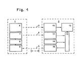
- the block diagram according to FIG. 1 of a device for optical information transmission between an identifier 1 and an identifier 2 shows on the one hand the various switching parts in the identifier 1 and in the identifier 2 and the optical contactless transmission paths 3, 4 and 5 between the two.
- the transmission paths 3 and 4 are directed on one side from the identifier 1 to the identifier 2, while the transmission path 5 can either be directed only on one side from the identifier 2 to the identifier 1 or on both sides between the two.
- the second option is indicated in the brackets.
- the identifier 1 consists of a first light source 6, which can emit infrared light via the transmission path 3. Another, similar to the first, but modulatable light source 7 in the identifier 1, which is controlled by a microprocessor 8, is assigned to the transmission path 4. A light-sensitive cell 9 in the identifier 1 is controlled via the transmission path 5, which transmits a signal to the microprocessor 8 for evaluation. Otherwise, the identifier 1 is designed in a known manner to query the identifier 2, i. H. e.g. B. with a slot for the introduction of the identifier 2 and optionally with transport, collection and devaluation means.
- the first light source 6 serves to supply the identifier 2 and is equipped for the emission of a continuous signal or an alternating signal.
- the second light source 7 generates coded light pulses for the transmission path 4 by the microprocessor 8.
- the various components in the identifier 1 are supplied with the necessary supply voltage by a built-in, not shown power supply unit.
- the identifier 2 advantageously consists of a multilayer plastic card in which an electronic circuit, integrated on a single chip, is embedded in a manner known per se.
- the electronic circuit in identifier 2 consists of a first receiving circuit 10, a second receiving circuit 11, an electrical energy conversion circuit 12, a microprocessor 13, a memory circuit 14 and one or more transmitter circuits 15.
- the first receiving circuit 10 contains a light-sensitive cell, for example a solar cell, photodiode or the like. When fed with a continuous light beam via the transmission path 3, this should be able to supply an output DC voltage of approximately one volt in a range from 10 to 100 microwatts. When supplied with alternating light with a frequency in the range of more than one hundred kHz, the light-sensitive cell should generate an alternating output voltage of approximately one volt, which is sieved by means of a capacitor of a suitable size.
- a sufficiently large voltage for operating the further electronic components is preferably achieved in the energy conversion circuit 12 by means of a chopper and, if appropriate, a voltage doubler circuit, followed by a rectifier.
- Such circuits are known and need not be described in detail. They serve primarily to operate the microprocessor 13, furthermore the memory circuit 14 and the transmitter circuit 15.
- the output voltage of the first receiving circuit 10 can also be converted in the energy conversion circuit 12 by means of ac / dc or dc / dc converters, stabilizers or similar circuits into a voltage suitable for the individual switching parts of the identifier 2 to be fed.
- the second receiving circuit 11 receives the coded light signals generated in the identifier 1 via the transmission path 4 and converts them into voltage pulses for further processing in the microprocessor 13 by means of a light-sensitive cell. It should The signal / noise ratio of the output pulses is better than 10 and the response time of the circuit required for this is better than 10 ms.
- the output signals of the second receiving circuit 11 are converted, possibly compared with information stored in the memory circuit 14, and output signals are generated for the control of the transmitter circuit 15. If desired, this can also consist of the stored information.
- the transmitter circuit 15 contains at least one controllable electronic-optical modulator, which is shown in FIGS. 2 to 4 and is subsequently described in more detail. It receives a continuous light beam generated in the identifier 1, which is modulated by means of the controllable electronic-optical modulator with the information to be transmitted from the identifier 2 in the microprocessor 13 to the identifier 1 and sent back to the identifier 1 to the photosensitive cell 9 thereof.
- the modulation can be caused by light attenuation or light scattering.
- the returned signal has a signal-to-noise ratio above 3 and a response time of less than 10 ms.
- the memory circuit 14 can perform various tasks. Memory with a minimum number of memory cells of more than 100 are sufficient for identifiers 2 which represent card-shaped, identifiable and / or voidable value units.
- the memory circuit 14 in both cases consists of an erasable PROM, for example an electrically reprogrammable PROM (EEPROM). If each identifier 2 is to be individualized in the last phase of production, a higher number of memory cells is also required.
- EEPROM electrically reprogrammable PROM
- the microprocessor 13 contains logic circuits which, in the simplest case, synchronize at least all functions of the chip.
- the number of logic functions essentially depends on the number of memory cells to be controlled in the memory circuit 14.
- the number of transmitter circuits 15 of the identifier 2 depends on whether a serial transmission or a parallel transmission is provided on the transmission path 5. In the first case, one can be satisfied with a single transmitter circuit 15. In the second case, one or more light sources in the identifier 1 corresponding to the number of parallel information and several transmitter circuits 15 in the identifier 2 are to be used.
- the transmitter circuit 15 consists of an infrared light modulating semiconductor element in MOS technology. Accordingly, a continuous infrared light source is provided in the identifier 1, which emits an infrared light beam which is intensity-modulated in the identifier 2 by the transmitter circuit 15.
- the transmitter circuit 15 according to FIG. 2 is constructed in four layers. On a heavily doped P + substrate 16, a P layer 17 is applied, which is covered by an SiO 2 layer 18 and is provided with a gate 19. The P + substrate 16 is connected to ground, while the gate 19 is supplied with a control voltage VG from the output of the microprocessor 13 of the identifier 2.
- the transmitter circuit 15 of the identifier 2 according to FIG. 2 acts in the following way:
- a continuous infrared light beam 20 is received by the identifier 1 through a first aperture provided in the identifier 2 in its surface layer which is not permeable to infrared light.
- the infrared light beam 20 can be a continuous light beam generated by the light source 6 of the identifier 1 and intended for the supply of the identifiers, or a continuous light beam generated in the identifier 1 by another light source, not shown.
- the light beam experiences a reduced weakening in its multiple reflections in the transmitter circuit 15 due to the absence of absorption by charge carriers.
- the coded attenuations of the light intensity represent the information to be transmitted from the identifier 2 to the identifier 1, which is transmitted to the microprocessor 8 by means of the light-sensitive cell 9 of the identifier 1 and processed there and, depending on the content of the information, triggers a switching operation.
- PN junction structure instead of a MOS structure, as in FIG. 2, a similar PN junction structure according to FIG. 3 can also be used in the semiconductor element of the transmitter circuit 15.
- a P layer 22 is arranged on a P + substrate 21 doped more with foreign atoms, into which a control electrode 23, which is more heavily doped with foreign atoms (N +), is embedded in a trough shape and a connecting wire 24 is soldered onto it.
- the P + substrate is connected to ground.
- an incoming infrared light beam 20 is refracted several times at the boundary layer of the P + substrate 21 and the control electrode 23 and leaves the semiconductor element of the transmitter circuit 15 as an infrared light beam 20a. If a positive control voltage is applied to the control electrode 23 by the microprocessor 13 of the identifier 2, the light beam which has been refracted several times in the semiconductor element is scattered, as a result of which the emerging infrared light beam 20a is less weakened. This changing weakening is significant for the information to be transmitted from identifier 2 to identifier 1.
- the semiconductor circuit of the transmitter circuit 15 of FIG. 4 is basically constructed in the same way as that of FIG. 3.
- the surface of the P layer 22 at points 22a and 22b is symmetrically chamfered relative to the vertical in such a way that the infrared light beam 20 that enters it and the emerging infrared light beam 20a can enter or exit perpendicular to the remaining surface of the P layer.
- the transmitter circuit 15 according to FIG. 4 acts in the same way as that of FIG. 3.
- the modulators according to FIGS. 2 to 4 can also be designed with complementary doping.
Landscapes
- Physics & Mathematics (AREA)
- Engineering & Computer Science (AREA)
- General Physics & Mathematics (AREA)
- Electromagnetism (AREA)
- Theoretical Computer Science (AREA)
- Computer Networks & Wireless Communication (AREA)
- Computer Hardware Design (AREA)
- Microelectronics & Electronic Packaging (AREA)
- Nonlinear Science (AREA)
- Radar, Positioning & Navigation (AREA)
- Optics & Photonics (AREA)
- Remote Sensing (AREA)
- Health & Medical Sciences (AREA)
- General Health & Medical Sciences (AREA)
- Toxicology (AREA)
- Artificial Intelligence (AREA)
- Computer Vision & Pattern Recognition (AREA)
- Optical Communication System (AREA)
- Credit Cards Or The Like (AREA)
- Radar Systems Or Details Thereof (AREA)
Description
- Die Erfindung bezieht sich auf eine Einrichtung zur kontaktlosen Informationsübertragung zwischen einem Identifikator und einem Identifikanden nach dem Oberbegriff des Patentanspruchs 1.
- Im folgenden sollen unter dem Begriff "Identifikand" nicht nur eine eigentliche Identifikationskarte, sondern auch kartenförmige, gegebenenfalls entwertbare Kredit-, Zutrittsberechtigungs-, Datenspeicherungs- oder für ähnliche Zwecke verwendbare Hilfsmittel verstanden werden.
- In der DE-OS-2031 085 ist eine Einrichtung nach dem Oberbegriff des Patentanspruchs 1 beschrieben, bei welcher gegebenenfalls die Stromversorgung einer im flächenförmigen Körper eingeschlossenen elektronischen Schaltung auf optischen Weg mit Hilfe einer Lichtquelle im Identifikator und einer Solarzelle im Identifikanden erfolgt. Außerdem sind lichtmodulierende Halbleiterelemente, die Infrarotlicht zwischen den Grenzflächen einer p-dotierten Grenzschicht mehrfach reflektieren, als solche aus US-A-3158 746 bekannt.
- Der Erfindung liegt die Aufgabe zugrunde, einen flachen Identifikator zu ermöglichen.
- Diese Aufgabe wird durch die Merkmale des Kennzeichens des Patentanspruchs 1 gelöst.
- Ausführungsbeispiele der Erfindung werden anhand einer Zeichnung näher erläutert. Es bedeuten:
- Fig. 1 ein Blockschema einer Einrichtung zur optischen Informationsübertragung zwischen einem Identifikator und einem Identifikanden und
- Fig. 2 bis 4 ein Halbleiterelement eines elektronisch-optischen Modulators in einem ldentifikanden.
- Das Blockschema nach der Fig. 1 einer Einrichtung zur optischen Informationsübertragung zwischen einem Identifikator 1 und einem Identifikanden 2 zeigt einerseits die verschiedenen Schaltteile im Identifikator 1 und im Identifikanden 2 und die optischen kontaktlosen Übertragungswege 3, 4 und 5 zwischen den beiden. Die Übertragungswege 3 und 4 sind einseitig vom Identifikator 1 zum Identifikanden 2 gerichtet, während der Übertragungsweg 5 entweder nur einseitig vom Identifikanden 2 zum Identifikator 1 oder beidseitig zwischen den beiden gerichtet sein kann. Die zweite Möglichkeit ist in der Klammer angedeutet.
- Der Identifikator 1 besteht aus einer ersten Lichtquelle 6, die Infrarotlicht über den Übertragungsweg 3 aussenden kann. Eine weitere, der ersten ähnliche, jedoch modulierbare Lichtquelle 7 im Identifikator 1, die von einem Mikroprozessor 8 gesteuert wird, ist dem Übertragungsweg 4 zugeordnet. Über den Übertragungsweg 5 wird eine lichtempfindliche Zelle 9 im Identifikator 1 angesteuert, welche ein Signal zur Auswertung zum Mikroprozessor 8 weiterleitet. Im übrigen ist der Identifikator 1 in bekannter Weise zur Abfrage des Identifikanden 2 ausgebildet, d. h. z. B. mit einem Schlitz zur Einführung des Identifikanden 2 und gegebenenfalls mit Transport-, Einzugs- und Entwertungsmitteln versehen.
- Die erste Lichtquelle 6 dient der Speisung des Identifikanden 2 und ist für die Ausstrahlung eines Dauersignals oder eines Wechselsignals ausgerüstet. Die zweite Lichtquelle 7 erzeugt durch den Mikroprozessor 8 kodierte Lichtimpulse für den Übertragungsweg 4. Die verschiedenen Bauteile im Identifikator 1 werden durch ein eingebautes, nichtgezeichnetes Netzteil mit der notwendigen Versorgungsspannung gespeist.
- Der Identifikand 2 besteht vorteilhaft aus einer mehrschichtigen Kunststoffkarte, in welcher eine elektronische Schaltung, auf einem einzigen Chip integriert, in an sich bekannter Weise eingebettet ist.
- Die elektronische Schaltung im Identifikanden 2 besteht aus einer ersten Empfangsschaltung 10, einer zweiten Empfangsschaltung 11, einer elektrischen Energieumwandlungsschaltung 12, einem Mikroprozessor 13, einer Speicherschaltung 14 und einer oder mehreren Senderschaltungen 15.
- Die erste Empfangsschaltung 10 enthält eine lichtempfindliche Zelle, beispielsweise eine Solarzelle, Photodiode oder ähnliches. Diese soll bei Speisung mit einem kontinuierlichen Lichtstrahl über den Übertragungsweg 3 eine Ausgangs-Gleichspannung von ungefähr einem Volt in einem Bereich von 10 bis 100 Mikrowatt liefern können. Bei Speisung mit Wechsellicht mit einer Frequenz im Bereich von über hundert kHz soll die lichtempfindliche Zelle eine Ausgangs-Wechselspannung von etwa einem Volt erzeugen, welche mittels eines Kondensators geeigneter Grösse gesiebt wird. Eine genügend grosse Spannung zum Betrieb der weiteren elektronischen Bauteile wird vorzugsweise mittels einer Zerhacker- und gegebenenfalls einer Spannungsverdopplerschaltung, gefolgt von einem Gleichrichter, in der Energieumwandlungsschaltung 12 erreicht. Solche Schaltungen sind bekannt und brauchen nicht näher beschrieben zu werden. Sie dienen in erster Linie zum Betrieb des Mikroprozessors 13, ferner der Speicherschaltung 14 und der Senderschaltung 15.
- Die Ausgangsspannung der ersten Empfangsschaltung 10 kann ferner in der Energieumwandlungsschaltung 12 mittels ac/dc oder dc/dc-Wandlern, Stabilisatoren oder ähnlichen Schaltungen in eine für die einzelnen zu speisenden Schaltteile des Identifikanden 2 angemessene Spannung umgeformt werden.
- Die zweite Empfangsschaltung 11 empfängt über den Übertragungsweg 4 die im Identifikator 1 erzeugten kodierten Lichtsignale und wandelt diese mittels einer lichtempfindlichen Zelle in Spannungsimpulse zur Weiterverarbeitung im Mikroprozessor 13 um. Dabei soll das Signal/Rauschverhältnis der Ausgangsimpulse besser als 10 und die Ansprechzeit der dazu benötigten Schaltung besser als 10 ms sein.
- Im Mikroprozessor 13 werden die Ausgangssignale der zweiten Empfangsschaltung 11 umgewandelt, gegebenenfals mit in der Speicherschaltung 14 gespeicherten Informationen verglichen und Ausgangssignale für die Ansteuerung der Senderschaltung 15 erzeugt. Diese können gewünschtenfalls auch aus den gespeicherten Informationen bestehen.
- Die Senderschaltung 15 enthält mindestens einen steuerbaren elektronisch-optischen Modulator, welcher in den Figuren 2 bis 4 dargestellt und anschliessend näher beschrieben wird. Sie empfängt einen im Identifikator 1 erzeugten kontinuierlichen Lichtstrahl, der mittels des steuerbaren elektronisch-optischen Modulators mit der im Mikroprozessor 13 des Identifikanden 2 von diesem zum Identifikator 1 zu übermittelnden Information moduliert und zum Identifikator 1 zu dessen lichtempfindlichen Zelle 9 zurückgesendet wird. Die Modulation kann durch Lichtschwächung oder Lichtstreuung bewirkt werden. Das zurückgesendete Signal hat ein Signal/Rauschverhältnis über 3 und eine Ansprechzeit von weniger als 10 ms.
- Die Speicherschaltung 14 kann verschiedene Aufgaben erfüllen. Für kartenförmige, Identifikations- und/oder entwertbare Werteinheiten darstellende Identifikanden 2 genügen Speicher mit einer minimalen Speicherzellenzahl von über 100.
- Wenn der Identifikand 2 dagegen hauptsächlich als Informationsspeicher dienen soll, sind entsprechend mehr Speicherzellen vorzusehen. Die Speicherschaltung 14 besteht in beiden Fällen aus einem löschbaren PROM, beispielsweise aus elektrisch umprogrammierbaren PROM (EEPROM). Wenn jeder Identifikand 2 in der letzten Phase der Herstellung individualisiert werden soll, ist ebenfalls eine höhere Speicherzellenzahl erforderlich.
- Der Mikroprozessor 13 enthält logische Schaltungen, die im einfachsten Fall zumindest alle Funktionen des Chips synchronisieren. Die Zahl der logischen Funktionen hängt im wesentlichen von der Zahl der in der Speicherschaltung 14 anzusteuernden Speicherzellen ab.
- Die Anzahl der Senderschaltungen 15 des Identifikanden 2 richtet sich danach, ob eine serielle Übertragung oder eine parallele Übertragung auf dem Übertragungsweg 5 vorgesehen ist. Im ersten Fall kann man sich mit einer einzigen Senderschaltung 15 begnügen. Im zweiten Fall sind eine oder mehrere, der Zahl der parallelen Informationen entsprechende Lichtquellen im Identifikator 1 und mehrere Senderschaltungen 15 im Identifikanden 2 zu benützen.
- Die Senderschaltung 15 nach der Fig. 2 besteht aus einem Infrarotlicht modulierenden Halbleiterelement in MOS-Technologie. Im Identifikator 1 ist dementsprechend eine kontinuierliche Infrarot-Lichtquelle vorgesehen, die einen Infrarot-Lichtstrahl aussendet, der durch die Senderschaltung 15 im Identifikanden 2 intensitätsmoduliert wird.
- Die Senderschaltung 15 nach Fig. 2 ist vierschichtig aufgebaut. Auf einem hochdotierten P+-Substrat 16 ist eine P-Schicht 17 aufgebracht, die von einer Si02-Schicht 18 überdeckt und mit einem Gate 19 versehen ist. Das P+-Substrat 16 wird mit Masse verbunden, während dem Gate 19 eine Steuerspannung VG vom Ausgang des Mikroprozessors 13 des Identifikanden 2 zugeführt wird.
- Die Senderschaltung 15 des Identifikanden 2 nach der Fig. 2 wirkt auf folgende Weise:
- Durch eine im Identifikanden 2 in dessen für Infrarotlicht nicht durchlässigen Oberflächenschicht vorgesehene erste Blende wird ein kontinuierlicher Infrarot-Lichtstrahl 20 vom Identifikator 1 empfangen. Der Infrarot-Lichtstrahl 20 kann ein von der Lichtquelle 6 des Identifikators 1 erzeugter kontinuierlicher und für die Speisung des Identifikanden bestimmter Lichtstrahl oder ein kontinuierlicher, von einer weiteren nichtgezeichneten Lichtquelle im Identifikator 1 erzeugter Lichtstrahl sein. Dieser wird nach seinem Eintritt in die für Infrarotlicht weitgehend transparente Si02-Schicht 18 der Senderschaltung 15 an dessen P+-Substrat 16 und der Schicht des Gate 19 mehrfach gebrochen und verlässt die Senderschaltung 15 durch eine nichtgezeichnete zweite Blende in der für Infrarotlicht nicht durchlässigen Oberflächenschicht des Identifikanden 2 als Infrarot-Lichtstrahl 20a. Dieser wird auf dem Übertragungsweg 5 zur lichtempfindlichen Zelle 9 des Identifikators 1 übertragen und dort detektiert.
- Wenn eine genügend grosse positive pulsartige Spannung VG an das Gate 19 der Senderschaltung 15 des Identifikanden 2 angelegt wird, erfährt der Lichtstrahl bei seinen mehrfachen Reflexionen in der Senderschaltung 15 infolge der wegfallenden Absorbtion durch Ladungs-Träger eine verminderte Abschwächung. Die kodierten Abschwächungen der Lichtintensität stellen die vom Identifikanden 2 zum Identifikator 1 zu übertragende Information dar, welche mittels der lichtempfindlichen Zelle 9 des Identifikators 1 zu dessen Mikroprozessor 8 übertragen und dort verarbeitet wird und je nach dem Inhalt der Information eine Schalthandlung auslöst.
- Anstelle einer MOS-Struktur, wie in der Fig. 2, kann auch eine ähnliche PN-Übergangsstruktur gemäss Fig. 3 im Halbleiterelement der Senderschaltung 15 verwendet werden.
- Bei dieser Halbleiterform ist auf einem stärker mit Fremdatomen dotierten P+-Substrat 21 eine P-Schicht 22 angeordnet, in die eine stärker mit Fremdatomen (N+) dotierte Steuerelektrode 23 wannenförmig eingelassen und auf dieser ein Anschlussdraht 24 aufgelötet ist. Das P+- Substrat ist mit Masse verbunden.
- Bei dieser Ausführungsform wird ein eintretender Infrarot-Lichtstrahl 20 mehrfach an der Grenzschicht des P+-Substrats 21 und der Steuerelektrode 23 gebrochen und verlässt das Halbleiterelement der Senderschaltung 15 als Infrarot-Lichtstrahl 20a. Wenn durch den Mikroprozessor 13 des Identifikanden 2 eine positive Steuerspannung an die Steuerelektrode 23 angelegt wird, erfährt der im Halbleiterelement mehrfach gebrochene Lichtstrahl eine Streuung, wodurch der austretende Infrarot-Lichtstrahl 20a weniger geschwächt wird. Diese wechselnde Schwächung ist signifikant für die vom Identifikanden 2 zum Identifikator 1 zu übertragende Information.
- Die Halbleiterschaltung der Senderschaltung 15 der Fig. 4 ist im Grunde gleich aufgebaut wie diejenige der Fig. 3. Dagegen ist die Oberfläche der P-Schicht 22 an den Stellen 22a und 22b derart gegenüber der Senkrechten symmetrisch abgeschrägt, dass der eintretende Infrarot-Lichtstrahl 20 und der austretende Infrarot-Lichtstrahl 20a senkrecht zur übrigen Oberfläche der P-Schicht ein- oder austreten können. Die Senderschaltung 15 nach Fig. 4 wirkt gleich wie diejenige der Fig. 3.
- Die Modulatoren gemäss den Fig. 2 bis 4 können auch mit komplementärer Dotierung ausgeführt werden.
Claims (9)
dadurch gekennzeichnet,
daß als Licht Infrarotlicht verwendet wird, im Identifikanden (2) alle elektronischen Schaltungen sowie die zugeordneten optischen Bauteile in einem einzigen, flächenförmigen, in den Identifikanden einschließbaren Chip integriert sind und dabei die dem Chip zugehörigen Senderschaltungen (15), die von einem dem Chip zugehörigen Mikroprozessor (13) steuerbare elektronisch-optische Modulatoren enthalten, als Halbleiterelemente ausgebildet sind und das Infrarotlicht zwischen den beiden Grenzflächen einer P-Schicht mehrfach reflektieren.
Priority Applications (1)
| Application Number | Priority Date | Filing Date | Title |
|---|---|---|---|
| AT85103632T ATE37964T1 (de) | 1984-05-03 | 1985-03-27 | Einrichtung zur kontaktlosen informationsuebertragung zwischen einem identifikator und einem identifikanden. |
Applications Claiming Priority (2)
| Application Number | Priority Date | Filing Date | Title |
|---|---|---|---|
| CH2150/84A CH663287A5 (de) | 1984-05-03 | 1984-05-03 | Einrichtung mit kontaktloser informationsuebertragung zwischen einem identifikator und einem identifikanden. |
| CH2150/84 | 1984-05-03 |
Publications (2)
| Publication Number | Publication Date |
|---|---|
| EP0166087A1 EP0166087A1 (de) | 1986-01-02 |
| EP0166087B1 true EP0166087B1 (de) | 1988-10-12 |
Family
ID=4227051
Family Applications (1)
| Application Number | Title | Priority Date | Filing Date |
|---|---|---|---|
| EP85103632A Expired EP0166087B1 (de) | 1984-05-03 | 1985-03-27 | Einrichtung zur kontaktlosen Informationsübertragung zwischen einem Identifikator und einem Identifikanden |
Country Status (5)
| Country | Link |
|---|---|
| US (1) | US4742573A (de) |
| EP (1) | EP0166087B1 (de) |
| AT (1) | ATE37964T1 (de) |
| CH (1) | CH663287A5 (de) |
| DE (1) | DE3565611D1 (de) |
Cited By (1)
| Publication number | Priority date | Publication date | Assignee | Title |
|---|---|---|---|---|
| EP0056064B1 (de) * | 1979-07-03 | 1990-10-10 | GAO Gesellschaft für Automation und Organisation mbH | Schaltungseinheit |
Families Citing this family (42)
| Publication number | Priority date | Publication date | Assignee | Title |
|---|---|---|---|---|
| USRE38419E1 (en) | 1986-05-13 | 2004-02-10 | Ncr Corporation | Computer interface device |
| GB2218237B (en) * | 1986-06-30 | 1991-01-16 | Wang Laboratories | Inductively-powered data storage card |
| DE3636414A1 (de) * | 1986-10-25 | 1988-05-05 | Messerschmitt Boelkow Blohm | Kontrollsystem zur identifizierung von personen und objekten |
| US4998294A (en) * | 1987-07-01 | 1991-03-05 | Moog Inc. | Opto-electrical power transmission and control system |
| US4837568A (en) * | 1987-07-08 | 1989-06-06 | Snaper Alvin A | Remote access personnel identification and tracking system |
| IT1211771B (it) * | 1987-09-11 | 1989-11-03 | Rinaldi Massimo | Sistema di controllo di traffico per mezzi mobili e/o persone utilizzante una stazione fissa ed un elemento programmabile portato da detti mezzi mobili e/o persone |
| US4916296A (en) * | 1987-10-29 | 1990-04-10 | Jerry R. Iggulden | Light modulating smart card |
| FR2632102B1 (fr) * | 1988-05-31 | 1992-07-17 | Tripeau Jean Pierre | Systeme de controle, notamment de controle d'acces a un lieu prive |
| GB8819481D0 (en) * | 1988-08-16 | 1988-09-21 | Plus 5 Eng Ltd | Portable memory device |
| US5239166A (en) * | 1989-01-17 | 1993-08-24 | Graves Marcel A | Secure data interchange system erasing a card memory upon an invalid response |
| EP0387383B1 (de) * | 1989-03-17 | 1995-05-24 | Siemens Aktiengesellschaft | Autarkes photonengetriebenes Bauelement |
| US5193201A (en) * | 1990-04-23 | 1993-03-09 | Tymes Laroy | System for converting a received modulated light into both power for the system and image data displayed by the system |
| FR2665008B1 (fr) * | 1990-07-20 | 1994-09-23 | Elgelec | Dispositif a infra-rouge comportant une fonction "reveil" de l'alimentation. |
| US5134282A (en) * | 1991-02-20 | 1992-07-28 | Cornell Research Foundation, Inc. | Optoelectric sensor and converter |
| DE4107452C1 (de) * | 1991-03-08 | 1992-07-23 | Orga Kartensysteme Gmbh, 6072 Dreieich, De | |
| DE4213881A1 (de) * | 1992-04-28 | 1993-11-04 | Bosch Gmbh Robert | System zur bidirektionalen datenuebertragung zwischen einer bake und einem fahrzeug |
| DE4213879A1 (de) * | 1992-04-28 | 1993-11-04 | Bosch Gmbh Robert | Kommunikationssystem zur datenuebertragung von einem bewegten fahrzeug auf eine ortsfeste bake |
| DE4213882A1 (de) * | 1992-04-28 | 1993-11-04 | Bosch Gmbh Robert | Vorrichtung eines fahrzeugs zur datenuebertragung auf eine ortsfeste bake und damit gebildetes kommunikationssystem |
| US5331453A (en) * | 1992-06-15 | 1994-07-19 | Ael Defense Corp. | Millimeter wave fiber-optically linked antenna receiver device |
| ES2080678B1 (es) * | 1994-01-11 | 1998-02-16 | Univ Madrid Politecnica | Sistema de identificacion que utiliza una tarjeta codificada alimentada a distancia. |
| FI110035B (fi) * | 1997-04-02 | 2002-11-15 | Juha Rapeli | Isäntälaitteen ja älykortin välisen kytkennän toteuttaminen |
| DE19959649A1 (de) * | 1999-12-10 | 2001-06-13 | Vlg Virtual Laser Systems Gmbh | Vorrichtung zur Erzeugung eines Antwortsignals aus einem Eingangssignal |
| AU2001275117A1 (en) * | 2000-06-06 | 2001-12-17 | Battelle Memorial Institute | Remote communication system and method |
| US7025277B2 (en) * | 2000-09-25 | 2006-04-11 | The Trustees Of Princeton University | Smart card composed of organic processing elements |
| DE10128655B4 (de) * | 2001-06-15 | 2005-12-15 | Orga Kartensysteme Gmbh | Chipkarte mit optischem Modulator und Verfahren zur Übertragung einer Information von einer Chipkarte |
| US6604685B1 (en) * | 2001-07-02 | 2003-08-12 | Bellsouth Intellectual Property Corporation | Optical smart card system, apparatus and method |
| US7003167B2 (en) * | 2001-11-01 | 2006-02-21 | Hewlett-Packard Development Company, L.P. | Single-pass guaranteed-fit data compression using rate feedback |
| KR20040054802A (ko) * | 2001-11-26 | 2004-06-25 | 내셔날 인스티튜트 오브 어드밴스드 인더스트리얼 사이언스 앤드 테크놀로지 | 무전원 단말에 의한 통신 시스템 |
| US6970089B2 (en) | 2002-07-03 | 2005-11-29 | Battelle Memorial Institute K1-53 | Full-spectrum passive communication system and method |
| SE0302191D0 (sv) * | 2003-03-10 | 2003-08-11 | Staffan Gunnarsson | Transponder med infrarödteknik |
| SE0300631D0 (sv) * | 2003-03-10 | 2003-03-10 | Staffan Gunnarsson | Transponder med solcell |
| US7564485B2 (en) * | 2003-09-29 | 2009-07-21 | Nattel Group, Inc. | Method for deactivating an image capturing device when present in a restricted or prohibited zone |
| US7065349B2 (en) * | 2003-09-29 | 2006-06-20 | Nattel Group, Inc. | Method for automobile safe wireless communications |
| US7230545B2 (en) * | 2003-11-07 | 2007-06-12 | Nattel Group, Inc. | Automobile communication and registry system |
| US7385484B2 (en) * | 2003-11-07 | 2008-06-10 | Sanjeev Nath | Method for automobile registry control system |
| US7451046B2 (en) * | 2004-04-29 | 2008-11-11 | Sanjeev Nath | Imminent collision warning system and method |
| WO2007036937A2 (en) * | 2005-09-27 | 2007-04-05 | Ortal Alpert | Directional light transmitter and receiver |
| EP3633824B1 (de) * | 2008-01-03 | 2025-05-14 | Wi-Charge Ltd. | Drahtloser laserleistungssender |
| US12254364B1 (en) * | 2009-10-08 | 2025-03-18 | Dynamics Inc. | Programming with light for powered cards and devices |
| US9369008B2 (en) | 2013-03-20 | 2016-06-14 | Nokia Technologies Oy | Method, apparatus, and computer program product for powering electronic devices |
| US9941741B2 (en) * | 2013-03-20 | 2018-04-10 | Nokia Technologies Oy | Method, apparatus, and computer program product for powering electronics in smart covers |
| CN112017341B (zh) * | 2020-07-17 | 2021-08-17 | 北京大学 | 一种基于逆反射可见光通信的物联网门禁系统 |
Citations (1)
| Publication number | Priority date | Publication date | Assignee | Title |
|---|---|---|---|---|
| DE2031085A1 (de) * | 1968-09-13 | 1971-01-14 | Intelectron Patentverwaltung GmbH, 8000 München | Identifizierungsschalter |
Family Cites Families (18)
| Publication number | Priority date | Publication date | Assignee | Title |
|---|---|---|---|---|
| GB868275A (en) * | 1959-09-18 | 1961-05-17 | Standard Telephones Cables Ltd | Improvements in or relating to light modulators |
| US3158746A (en) * | 1960-12-27 | 1964-11-24 | Sprague Electric Co | Light modulation in a semiconductor body |
| NL269289A (de) * | 1961-09-15 | |||
| US3153691A (en) * | 1962-04-12 | 1964-10-20 | Bell Telephone Labor Inc | Light modulator |
| US3584220A (en) * | 1966-04-09 | 1971-06-08 | Hitachi Ltd | Optical communication system |
| FR1499441A (fr) * | 1966-09-16 | 1967-10-27 | Electronique & Physique | Procédé et dispositif de transmission d'informations sur faisceau lumineux |
| FR1603131A (de) * | 1968-07-05 | 1971-03-22 | ||
| FR2048067B2 (de) * | 1969-06-30 | 1973-01-12 | Dethloff Juergen | |
| GB1529789A (en) * | 1974-08-16 | 1978-10-25 | Chubb & Sons Lock & Safe Co | Security systems |
| US3951513A (en) * | 1974-09-09 | 1976-04-20 | Masi James V | Semiconductor light modulating optical wave guide |
| DE2453077B2 (de) * | 1974-11-08 | 1976-09-02 | Precitronic Gesellschaft für Feinmechanik und Electronic mbH, 2000 Hamburg | Empfangs-sendeeinrichtung fuer die informationsuebermittlung mittels gebuendelter, modulierter lichtstrahlen |
| US3989942A (en) * | 1974-12-13 | 1976-11-02 | International Telephone And Telegraph Corporation | Retro-reflecting laser responser and data modulator |
| GB1567750A (en) * | 1975-09-19 | 1980-05-21 | Seldown Electronics Ltd | Transponders |
| US4114151A (en) * | 1976-09-14 | 1978-09-12 | Alfa-Laval Company Limited | Passive transponder apparatus for use in an interrogator-responder system |
| SE418909B (sv) * | 1978-03-02 | 1981-06-29 | Saab Scania Ab | Sett och anleggning for att medelst modulerad optisk stralning overfora information till foremal |
| DE2919753A1 (de) * | 1979-05-16 | 1980-11-27 | Bbc Brown Boveri & Cie | Einrichtung zur automatischen identifizierung von objekten und/oder lebewesen |
| US4479264A (en) * | 1982-04-26 | 1984-10-23 | Geosource Inc. | Transducer for optical data transmission |
| US4432614A (en) * | 1982-12-20 | 1984-02-21 | Gte Laboratories Incorporated | High frequency light modulator |
-
1984
- 1984-05-03 CH CH2150/84A patent/CH663287A5/de not_active IP Right Cessation
-
1985
- 1985-03-27 EP EP85103632A patent/EP0166087B1/de not_active Expired
- 1985-03-27 AT AT85103632T patent/ATE37964T1/de not_active IP Right Cessation
- 1985-03-27 DE DE8585103632T patent/DE3565611D1/de not_active Expired
- 1985-04-25 US US06/727,271 patent/US4742573A/en not_active Expired - Fee Related
Patent Citations (1)
| Publication number | Priority date | Publication date | Assignee | Title |
|---|---|---|---|---|
| DE2031085A1 (de) * | 1968-09-13 | 1971-01-14 | Intelectron Patentverwaltung GmbH, 8000 München | Identifizierungsschalter |
Cited By (1)
| Publication number | Priority date | Publication date | Assignee | Title |
|---|---|---|---|---|
| EP0056064B1 (de) * | 1979-07-03 | 1990-10-10 | GAO Gesellschaft für Automation und Organisation mbH | Schaltungseinheit |
Also Published As
| Publication number | Publication date |
|---|---|
| DE3565611D1 (en) | 1988-11-17 |
| EP0166087A1 (de) | 1986-01-02 |
| CH663287A5 (de) | 1987-11-30 |
| ATE37964T1 (de) | 1988-10-15 |
| US4742573A (en) | 1988-05-03 |
Similar Documents
| Publication | Publication Date | Title |
|---|---|---|
| EP0166087B1 (de) | Einrichtung zur kontaktlosen Informationsübertragung zwischen einem Identifikator und einem Identifikanden | |
| EP0056064A1 (de) | Schaltungseinheit | |
| DE69026436T2 (de) | Fotoelektrische Wandler mit Belichtungssystem und damit ausgerüstetes Informationsverarbeitungsgerät | |
| DE3724248C2 (de) | ||
| DE971860C (de) | Wechselstrom-Steuerschaltung | |
| DE69721335T2 (de) | Datenaustauschvorrichtung mit kontakt- und kontaktloser betriebsart | |
| DE69634025T2 (de) | Vorrichtung für die Ableitung einer Restladung in einem Bildaufnahmesystem | |
| DE69228144T2 (de) | Elektronisches Etikett | |
| DE69310900T2 (de) | Integrierte lichtemittierende und lichtdetektierende festkoerperanordnung und vorrichtung die eine solche anordnung verwendet. | |
| DE69310965T2 (de) | Vorrichtung zum Übertragen von elektrischen Signalen und Versorungsleistung zu einem Datenspeicher einer Kassette. | |
| EP0387383A1 (de) | Autarkes photonengetriebenes Bauelement | |
| DE19509517C1 (de) | Vorrichtung, bestehend aus mindestens einem Kartenendgerät zur Übertragung von Energie zu einer Chipkarte und zum Datenaustausch mit der Chipkarte über elektromagnetische Wellen | |
| DE2747076B2 (de) | Optoelektrischer Code-Kartenleser | |
| DE69520408T2 (de) | Elektronisches etikett zum optischen lesen/schreiben | |
| EP0095998A1 (de) | Faseroptische Messanordnung | |
| EP0025956A2 (de) | Optische Vorrichtung zum berührungslosen Schreiben | |
| DE2135448C3 (de) | Lichtaussendende Halbleitereinrichtung | |
| EP1850481A1 (de) | Leuchtmittel mit mehreren LEDs und einem sensitiven Schalter | |
| DE3715199A1 (de) | Chipkartensystem | |
| DE102011056614B4 (de) | Verfahren zur Datenübertragung zwischen einem Datenträger und einer Datenstation mittels Übertragen von Energie durch Licht und Übertragen von Daten durch Licht, Datenträger und Datenstation zur Verwendung in dem Verfahren | |
| EP0889447B1 (de) | Optischer Sensor in Münzprüfanordnungen | |
| DE102021116814A1 (de) | Optoelektronische sensorvorrichtung | |
| CH662225A5 (de) | Opto-elektronische anordnung zur speisung einer elektronischen schaltung mit licht. | |
| DE2748292A1 (de) | Vorrichtung zum uebertragen von signalen | |
| DE19535199A1 (de) | Chipkarte mit optischer Schnittstelle |
Legal Events
| Date | Code | Title | Description |
|---|---|---|---|
| PUAI | Public reference made under article 153(3) epc to a published international application that has entered the european phase |
Free format text: ORIGINAL CODE: 0009012 |
|
| AK | Designated contracting states |
Designated state(s): AT DE FR GB IT SE |
|
| 17P | Request for examination filed |
Effective date: 19860624 |
|
| 17Q | First examination report despatched |
Effective date: 19870908 |
|
| GRAA | (expected) grant |
Free format text: ORIGINAL CODE: 0009210 |
|
| AK | Designated contracting states |
Kind code of ref document: B1 Designated state(s): AT DE FR GB IT SE |
|
| REF | Corresponds to: |
Ref document number: 37964 Country of ref document: AT Date of ref document: 19881015 Kind code of ref document: T |
|
| GBT | Gb: translation of ep patent filed (gb section 77(6)(a)/1977) | ||
| REF | Corresponds to: |
Ref document number: 3565611 Country of ref document: DE Date of ref document: 19881117 |
|
| ET | Fr: translation filed | ||
| ITF | It: translation for a ep patent filed | ||
| PLBE | No opposition filed within time limit |
Free format text: ORIGINAL CODE: 0009261 |
|
| STAA | Information on the status of an ep patent application or granted ep patent |
Free format text: STATUS: NO OPPOSITION FILED WITHIN TIME LIMIT |
|
| 26N | No opposition filed | ||
| ITTA | It: last paid annual fee | ||
| REG | Reference to a national code |
Ref country code: GB Ref legal event code: 746 |
|
| PGFP | Annual fee paid to national office [announced via postgrant information from national office to epo] |
Ref country code: GB Payment date: 19930222 Year of fee payment: 9 |
|
| PGFP | Annual fee paid to national office [announced via postgrant information from national office to epo] |
Ref country code: AT Payment date: 19930303 Year of fee payment: 9 |
|
| PGFP | Annual fee paid to national office [announced via postgrant information from national office to epo] |
Ref country code: FR Payment date: 19930305 Year of fee payment: 9 |
|
| PGFP | Annual fee paid to national office [announced via postgrant information from national office to epo] |
Ref country code: SE Payment date: 19930312 Year of fee payment: 9 |
|
| PGFP | Annual fee paid to national office [announced via postgrant information from national office to epo] |
Ref country code: DE Payment date: 19930423 Year of fee payment: 9 |
|
| PG25 | Lapsed in a contracting state [announced via postgrant information from national office to epo] |
Ref country code: GB Effective date: 19940327 Ref country code: AT Effective date: 19940327 |
|
| PG25 | Lapsed in a contracting state [announced via postgrant information from national office to epo] |
Ref country code: SE Free format text: LAPSE BECAUSE OF NON-PAYMENT OF DUE FEES Effective date: 19940328 |
|
| GBPC | Gb: european patent ceased through non-payment of renewal fee |
Effective date: 19940327 |
|
| PG25 | Lapsed in a contracting state [announced via postgrant information from national office to epo] |
Ref country code: FR Effective date: 19941130 |
|
| PG25 | Lapsed in a contracting state [announced via postgrant information from national office to epo] |
Ref country code: DE Effective date: 19941201 |
|
| REG | Reference to a national code |
Ref country code: FR Ref legal event code: ST |
|
| EUG | Se: european patent has lapsed |
Ref document number: 85103632.7 Effective date: 19941010 |