EP0163394A2 - Dispositif de focalisation automatique - Google Patents
Dispositif de focalisation automatique Download PDFInfo
- Publication number
- EP0163394A2 EP0163394A2 EP85302502A EP85302502A EP0163394A2 EP 0163394 A2 EP0163394 A2 EP 0163394A2 EP 85302502 A EP85302502 A EP 85302502A EP 85302502 A EP85302502 A EP 85302502A EP 0163394 A2 EP0163394 A2 EP 0163394A2
- Authority
- EP
- European Patent Office
- Prior art keywords
- arrays
- sensor
- image
- array
- arrangement according
- Prior art date
- Legal status (The legal status is an assumption and is not a legal conclusion. Google has not performed a legal analysis and makes no representation as to the accuracy of the status listed.)
- Granted
Links
- 238000003491 array Methods 0.000 claims abstract description 41
- 230000003287 optical effect Effects 0.000 claims abstract description 13
- 238000000034 method Methods 0.000 claims description 5
- 239000000758 substrate Substances 0.000 claims description 5
- 238000006243 chemical reaction Methods 0.000 claims description 4
- 238000010191 image analysis Methods 0.000 description 3
- 230000000694 effects Effects 0.000 description 2
- 239000002184 metal Substances 0.000 description 2
- 238000012216 screening Methods 0.000 description 2
- 238000004458 analytical method Methods 0.000 description 1
- 125000004122 cyclic group Chemical group 0.000 description 1
- 238000005286 illumination Methods 0.000 description 1
- 238000012886 linear function Methods 0.000 description 1
- 230000000717 retained effect Effects 0.000 description 1
- 238000000926 separation method Methods 0.000 description 1
- 230000007704 transition Effects 0.000 description 1
- 230000001960 triggered effect Effects 0.000 description 1
- 238000011179 visual inspection Methods 0.000 description 1
Images


Classifications
-
- G—PHYSICS
- G02—OPTICS
- G02B—OPTICAL ELEMENTS, SYSTEMS OR APPARATUS
- G02B21/00—Microscopes
- G02B21/24—Base structure
- G02B21/241—Devices for focusing
- G02B21/244—Devices for focusing using image analysis techniques
Definitions
- THE PRESENT INVENTION relates to an automatic focussing device and more particularly, although not exclusively, to an automatic focussing device suitable for use with an image analysis system, such as an image analysis system used to analyse the nature of cells present on a slide.
- an image analysis system such as an image analysis system used to analyse the nature of cells present on a slide.
- Such a device may be used, for example, in a cervical cytolosy pre-screening programme. Whilst such an arrangement will incorporate a microscope to be focussed, the invention may find applications in other devices which require optical focussing such as projectors, cameras and the like.
- the device consisted of a beam splitter attachment for use with an appropriate microscope, the beamsplitter serving to split the image beam into three separate beams. Each part of the split beam is directed towards a respective image sensor. One sensor is located on the main focal plane of the relevant beam, and the other two sensors are located respectively just short of and just beyond the main focal plane of the respective beams.
- a focus error signal is derived from the sensors which consists of a suitable non-linear function of illumindtion which favours dark/light transitions at the edges of the. objects and within objects. This is integrated for each sensor over the same field of view, since at any instant the same image portion is directed towards the three sensors.
- This integral will be a maximum for a sensor on which an image is sharply focussed, and the value of the integral provided by two sensors which are equally out of focus will be the same. Consequently the focussing of the arrangement can be adjusted so that the value of the integral derived from the main sensor is at a maximum, and the value of the integrals obtained from the remaining two sensors is equal.
- an automatic focussing arrangement incorporated in a system in which an optical image is focussed onto a focus plane, comprising a sensor assembly located in the region of the focus plane to sense the image, the sensor assembly comprising at least two arrays of sensor devices, one array of sensor devices being in front of the focus plane, and the second array of sensor devices being behind the focus plane, means being provided for effecting relative movement between the image and to the sensor assembly, means being provided for deriving from the first and second arrays signals representative of the image received by the said sensor devices, and for deriving, from those signals, a focus drive signal to maintain the focus of the arrangement as desired.
- the invention may be used to focus a microscope ready for visual inspection of a slide by an operator.
- the invention is used where the image is sensed by part of the system so that the system may perform at least a preliminary screening of the slides to be inspected.
- a further array of sensor devices or some other sensor arrangement, such as a camera is provided, which is located in a focus plane, to sense the focussed image.
- the arrays of sensor devices are all mounted on a single substrate which is tilted relative to said focus plane, the first and second arrays being located in regions of the substrate that are in front of and behind said focus plane respectively.
- the arrays may all form part of a single "chip" of arrays, or may be totally separate arrays mounted on said single substrate in the appropriate relative positions.
- Each array may comprise an array of charge coupled devices.
- the arrays are elongate arrays and the relative movement between the sensor assembly and said image in said focus plane is in a direction transverse to the longitudinal axes of said arrays.
- the arrangement further comprises means for deriving a signal representative of the contrast of part of the image as viewed by the one of the first and second arrays, means for storing the information at least until such time that the other of the arrays respectively senses the same part of the image, and means for comparing the information from the said arrays to derive said focus drive signal.
- the first and second sensor arrays each consist of a plurality of sensing elements adapted to provide output signals representative of the levels of light intensity received by adjacent or next adjacent sensing elements, said deriving means including means to calculate the difference between signals from said first and second arrays to provide a signal representative of contrast.
- an analog output signal from each of the first and second arrays is passed through an analog to digital converter to create a digital signal.
- each digital signal is subjected to a logarithmic conversion process prior to said subtraction process. This serves to reduce the dependance of the calculated value on the incident illumination.
- each of the first and second sensor arrays comprises two staggered rows of light sensitive devices, signals from one of the rows of the said first array being processed and signals from the other of the rows of the second array being processed, thus enabling the same processing circuitry to be utilised for the first and second arrays.
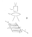
- an optical system includes an adjustable focussing device I and a lens system 2.
- Figure is purely a diagrammatic figure in this respect.
- the combination of the focussing device I and the lens system 2 is intended to focus an image in a plane (which is called "the focus plane") located in the region of a sensor array 3.
- the sensor array 3 is movable transversely in the direction shown by the arrows 4, 5 across said plane and thus the sensor array can be physically moved across the entire image. Whilst, in the presently described embodiment the sensor is caused to move relative to the image it is to be understood that in an alternative embodiment of the invention the image may be moved relative to the sensor.
- the sensor consists of a single chip which has on it three arrays 6, 7, 8 of charge coupled devices, each array 6, 7, 8 comprising two staggered adjacent rows of charge coupled devices.
- the chip carrying the arrays of charge coupled devices is located so that the charge coupled devices extend perpendicularly to the direction of movement of the chip as indicated by the arrows 4, 5. Also, the chip is tilted slightly relative to the focus plane so that a first array of charge coupled devices (array 8) is slightly in front of the focus plane and a second array, 6, is located slightly behind the focus pl ⁇ ne. The angle of tilt is about 15 0 . The central array 7 actually lies on the focus plane.
- each array of charge coupled devices will "see” the same “scan line” of the image in turn.
- the array 7 of the charge coupled devices will have the image to be viewed perfectly focussed upon it, and the arrays 6 and 8 will both "see” the image out of focus, the array 8 "seeing” the image in what can be termed under focus and the array 6 "seeing" the image in what can be termed over focus.
- the array 8 when the array 8 first "sees” a scan line or other image area, information relating to the measured contrast in that scan line or image area is determined and stored.
- the sensor 3 When the sensor 3 has been moved by such a distance relative to the image that the array 6 is then "seeing" the same scan line or image area corresponding information is derived from the array 6, that information is compared with the information that has been derived from the array 6, and stored. The comparison of the two items of information enables a focus correcting signal to be generated, which can be fed to the adjustable focussing device I.
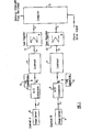
- channel A commences with the image sensor 8 which consists of the above- described "first array" of charge coupled devices
- image sensor 6 which is the "second array” of charge coupled devices mentioned above.
- the distance in the direction of intended movement of the sensor is approximately 280 microns.
- the angle of tilt of the chip the two image sensors are displaced in focus by about 3 microns from each other.
- the sensor 8 is 1.5 microns in front of the focus plane
- the sensor 6 is 1.5 microns behind the focus plane.
- each image sensor which is constituted by an array of charge coupled devices is a series of analog signals each representing the light intensity falling on a respective one of the charge coupled devices, i.e. on a respective pixel of the image.
- Each channel includes an analog to digital converter 9 which converts the analog output from the linear image sensor to an 8-bit digital value.
- the signal After the signal has passed through the analog to digital converter 9, the signal is subjected to a logarithmic conversion 10. The signal is thus converted from a signal representing a measured light level to a signal representing a nominal optical density. This conversion is not thought to be strictly necessary, but it is believed that this will help reduce the variation in the contrast measured with variations in the overall light level.
- the signals derived from next adjacent pixels or next adjacent charge coupled devices are subtracted. Such an arrangement is used rather than taking the difference between immediately adjacent pixels or immediately adjacent charge coupled devices because one particular charge coupled device array that may be utilised has separate channels for "Odd” and "Even” pixels and thus the arrangement that we propose to utilise is facilitated.
- the differences between the signals derived from next adjacent pixels are thus determined.
- the contrast measure may be determined by subtracting a constant value from the difference. All values that are not positive are then deemed to be zero.
- the resultant values may be raised to a power of, for-example, 1.5 and multiplied by a further constant to provide a contrast value for each of the next adjacent pairs of pixels.
- contrast values when determined in blocks I are passed to scan registers 12 where they are stored and summed, and the summed values are then passed to a computer 13.
- each scan register would accummulate for ever, and eventually overflow unless specific steps were taken to avoid this happening. Consequently the signals present in this scan register are read out at regular intervals, triggered whenever the sensor assembly 3 has been physically moved to a predetermined distance. In one embodiment this distance is set to be 70 microns, since it is most conveniently a sub-multiple of the array separation. Thus, after four interrupts (i.e. four separate step- like movements of the sensor) the array 6 is scanning the ' same image as array 8, if the array 8 is leading, and vice-versa in the opposite scan direction.
- Each sample of signals taken from the scan registers represents the integrated contrast measure of the area defined by the width of the scan line (e.g. 1024 microns) and the distance travelled by the sensor since the previous reading (70 microns). It is thus possible to compare the contrast measure readings of channel A and channel B for the same area by using a shift register, or cyclic buffer, in the computer to hold one set of samples for four interrupts before comparison is effected.
- the computer is provided with signals indicating each distance interrupt of movement of the sensor 3, and the computer provides an output which is a focus drive signal.
- the described embodiment may be simplified or improved to a certain extent if the charge coupled device arrays each consist of staggered rows of charge coupled devices, and if only the "Even” devices are used from channel A and only the “Odd” devices are used from channel B, since it is then possible to utilise exactly the same analog to digital converter, logarithmic converter and contrast calculator for the two channels. This obviates any risk of lack of balance between the two channels which is an advantage, since it will be understood that lack of balance between the two channels can contribute to poor focus.
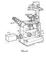
- Figures 3 and 4 illustrates a microscope provided with a focussing system in accordance with the invention.
- the microscope 15 is of conventional design and is provided with a lamp housing 16 containing a lamp which directs light, from a lamp within the housing, through a diaphragm t7, towards a condensor assembly 18. The tight then passes through a specimen 19 retained by specimen clips 20 on a movable specimen stage plate 21. The light then passes through an objective lens present on a revolving nosepiece 22 and then passes into an optical system contained within a supporting housing 23.
- a focussing control 24 is provided to enable the optical system to be manually focussed if desired, but, as will be described, the microscope is provided with an automatic focussing system in accordance with the invention.
- the movable stage plate is driven by means of a motor contained within a motor housing 25.
- the motor may be manually controlled by means of appropriate knobs or switches 26, 27 to control manually movement of the specimen stage plate in the "X" and "Y” directions.
- the motor may also be controlled automatically.
- the microscope is provided with three optical outputs.
- the beam within the microscope is passed through a beam splitter and three beams are created each with its own focus plane.
- Each optical output is coaligned with a respective focus plane.
- the first output is connected to a binocular eyepiece tube 28 to enable an image of the specimen to be viewed by eye.
- a second output 29 is in the form of a camera port adapted to be connected to a camera 30 or other image sensing device, such as an array of charge coupled devices, to enable the image of the specimen to be "viewed" electronical ly.
- the third port, 31, is operatively connected to a sensor 3 in accordance with the present invention.
- the sensor 3 is formed on the front face of an integrated circuit 32 having rearwardly extending legs 33 which lie on either side of a metal strip 34 which is in contact with the undersurface of the integrated circuit 32 and thus constitutes a heat sink for the sensor.
- the metal strip 34 is formed integrally with and extends partly across the centre of a square frame 35 provided with two screw holes 36.
- a smaller square frame 37, with holes 38 at the corners thereof is secured by means of screws 39 to the front face of the frame 35 and facilitates the location of the frame 35, and the sensor 3, on an inclined face 40 of a sensor carrier 41.
- the sensor carrier 41 has a tubular spigot 42 which carries a transverse head 43, the end face of which 40 is inclined at an angle of approximatley 15 0 to the axis defined by the spigof 42.
- a square recess 44 is formed in the inclined face 40 which is dimensioned to receive the frame 37.
- the face 40 is also provided with two internally threaded bores 45 adapted to receive screws passing through the screw holes 36 formed in the frame 35.
- the frame 35 is thus located in position with the frame 37 received snugly within the square recess 44, and screws are then passed through the screw holes 36 into the internally threaded bores 45 to secure the frame 35 in position, and thus to secure the sensor 3 in position.
- the sensor 3 is thus secured in position with the front face thereof, which carries the sensor array described above, inclined at an angle of 15 0 to the axis of the spigot 42.
- the spigot 42 is, of course, hollow to permit a beam of light to pass up the spigot and fall onto the sensor 3.
- the spigot 42 of the sensor carrier 41 is received within a further tubular spigot 46 of a holding assembly 47.
- the holding assembly 47 consists of a tubular spigot 46 and a transverse circular head 48 provided with two axially extending diammetricatty opposed apertures 49 and a radially extending aperture 50 which receives a grub screw 51.
- the spigot 42 may be inserted into the hollow interior of the spigot 46 and when the sensor carrier 41 has been rotated to a desired position the grub screw 51 may be tightened.
- the holding assembly 47 may be secured to a mounting plate 52 by means of screws passing through the apertures 49 in the circular head 48 of the assembly, these screws being received in screw threaded apertures 53 formed in the plate 52.
- the apertures 53 lie on diametrically opposed sides of a relatively large aperture 54 dimensioned to receive the spigot 46.
- the plate 52 may be secured to the body of the microscope by means of mounting strips 55 provided with apertures 56 to receive screws which can be received in appropriate screw threaded bores provided within the housing 23 of the microscope.
- the sensor carrier assembly 41 may be rotated so that the various sensor arrays provided on the sensor 3 lie in the desired position.
- the various components will be designed so that when installed in the manner described the focus plane will lie on the central sensor array provided on the sensor 3.
- the image is moved relative to the sensor. This is achieved by actually moving the specimen by means of a motor contained within the motor housing 25. The motor is thus controlled automatically to effect the desired stepping movement of the specimen whilst the focussing of the arrangment is automatically accomplished. The focussed image may then be viewed through the binocular eyepiece 28 or the specimen may be "viewed" by the camera or other sensor 30.
- the focussing system of the invention may find various other applications in the focussing of projectors, cameras or other optical devices where images have to be brought into focus.
Landscapes
- Physics & Mathematics (AREA)
- Optics & Photonics (AREA)
- Chemical & Material Sciences (AREA)
- Analytical Chemistry (AREA)
- Computer Vision & Pattern Recognition (AREA)
- General Physics & Mathematics (AREA)
- Engineering & Computer Science (AREA)
- Automatic Focus Adjustment (AREA)
- Focusing (AREA)
- Inorganic Insulating Materials (AREA)
- Window Of Vehicle (AREA)
- Eye Examination Apparatus (AREA)
- Earth Drilling (AREA)
Priority Applications (1)
| Application Number | Priority Date | Filing Date | Title |
|---|---|---|---|
| AT85302502T ATE68271T1 (de) | 1984-04-16 | 1985-04-09 | Automatische fokussiereinrichtung. |
Applications Claiming Priority (2)
| Application Number | Priority Date | Filing Date | Title |
|---|---|---|---|
| GB8409855 | 1984-04-16 | ||
| GB8409855 | 1984-04-16 |
Publications (3)
| Publication Number | Publication Date |
|---|---|
| EP0163394A2 true EP0163394A2 (fr) | 1985-12-04 |
| EP0163394A3 EP0163394A3 (en) | 1987-10-28 |
| EP0163394B1 EP0163394B1 (fr) | 1991-10-09 |
Family
ID=10559711
Family Applications (1)
| Application Number | Title | Priority Date | Filing Date |
|---|---|---|---|
| EP85302502A Expired - Lifetime EP0163394B1 (fr) | 1984-04-16 | 1985-04-09 | Dispositif de focalisation automatique |
Country Status (5)
| Country | Link |
|---|---|
| US (1) | US4636051A (fr) |
| EP (1) | EP0163394B1 (fr) |
| JP (1) | JPS60238805A (fr) |
| AT (1) | ATE68271T1 (fr) |
| DE (1) | DE3584314D1 (fr) |
Cited By (7)
| Publication number | Priority date | Publication date | Assignee | Title |
|---|---|---|---|---|
| FR2605751A1 (fr) * | 1986-10-22 | 1988-04-29 | Bioconcept Sarl | Dispositif pour la mise au point automatique d'un microscope |
| DE3728257A1 (de) * | 1986-11-06 | 1988-05-11 | Jenoptik Jena Gmbh | Optische anordnung und verfahren zur lichtelektrischen entfernungseinstellung, insbesondere fuer operationsmikroskope |
| EP0529458A1 (fr) * | 1991-08-22 | 1993-03-03 | Applied Imaging International Ltd. | Système automatique de mise au point |
| WO1996001438A1 (fr) * | 1994-07-01 | 1996-01-18 | Price Jeffrey H | Systeme de focalisation automatique pour microscopie a balayage |
| US5790710A (en) * | 1991-07-12 | 1998-08-04 | Jeffrey H. Price | Autofocus system for scanning microscopy |
| US5790692A (en) * | 1994-09-07 | 1998-08-04 | Jeffrey H. Price | Method and means of least squares designed filters for image segmentation in scanning cytometry |
| US5932872A (en) * | 1994-07-01 | 1999-08-03 | Jeffrey H. Price | Autofocus system for scanning microscopy having a volume image formation |
Families Citing this family (7)
| Publication number | Priority date | Publication date | Assignee | Title |
|---|---|---|---|---|
| JPH07117645B2 (ja) * | 1987-12-14 | 1995-12-18 | キヤノン株式会社 | 焦点検出装置 |
| US5697885A (en) * | 1989-01-30 | 1997-12-16 | Olympus Optical Co., Ltd. | Endoscope for recording and displaying time-serial images |
| US5912699A (en) * | 1992-02-18 | 1999-06-15 | Neopath, Inc. | Method and apparatus for rapid capture of focused microscopic images |
| US5642433A (en) * | 1995-07-31 | 1997-06-24 | Neopath, Inc. | Method and apparatus for image contrast quality evaluation |
| WO2016055176A1 (fr) * | 2014-10-06 | 2016-04-14 | Leica Microsystems (Schweiz) Ag | Microscope |
| JP6805135B2 (ja) | 2014-10-06 | 2020-12-23 | ライカ マイクロシステムズ (シュヴァイツ) アクチエンゲゼルシャフトLeica Microsystems (Schweiz) AG | 顕微鏡 |
| WO2016055177A1 (fr) * | 2014-10-06 | 2016-04-14 | Leica Microsystems (Schweiz) Ag | Microscope |
Citations (3)
| Publication number | Priority date | Publication date | Assignee | Title |
|---|---|---|---|---|
| US4203031A (en) * | 1977-03-23 | 1980-05-13 | Olympus Optical Co., Ltd. | Automatic focussing apparatus for microscope |
| US4314150A (en) * | 1978-11-01 | 1982-02-02 | Olympus Optical Company Limited | Apparatus for detecting the in-focusing conditions |
| EP0054349A2 (fr) * | 1980-12-10 | 1982-06-23 | EMI Limited | Système optique à mise au point automatique |
Family Cites Families (5)
| Publication number | Priority date | Publication date | Assignee | Title |
|---|---|---|---|---|
| JPS5557809A (en) * | 1978-10-24 | 1980-04-30 | Olympus Optical Co Ltd | Focusing detection system |
| US4349254A (en) * | 1979-02-13 | 1982-09-14 | Asahi Kogaku Kogyo Kabushiki Kaisha | Camera focus detecting device |
| JPS55146424A (en) * | 1979-05-02 | 1980-11-14 | Olympus Optical Co Ltd | Photodetector for focus detection |
| JPS5772116A (en) * | 1980-10-23 | 1982-05-06 | Canon Inc | Signal processing circuit for focus detector |
| JPS5919913A (ja) * | 1982-07-26 | 1984-02-01 | Nippon Kogaku Kk <Nikon> | 焦点制御装置 |
-
1985
- 1985-04-09 AT AT85302502T patent/ATE68271T1/de not_active IP Right Cessation
- 1985-04-09 DE DE8585302502T patent/DE3584314D1/de not_active Expired - Fee Related
- 1985-04-09 EP EP85302502A patent/EP0163394B1/fr not_active Expired - Lifetime
- 1985-04-15 US US06/723,611 patent/US4636051A/en not_active Expired - Fee Related
- 1985-04-16 JP JP60081215A patent/JPS60238805A/ja active Pending
Patent Citations (3)
| Publication number | Priority date | Publication date | Assignee | Title |
|---|---|---|---|---|
| US4203031A (en) * | 1977-03-23 | 1980-05-13 | Olympus Optical Co., Ltd. | Automatic focussing apparatus for microscope |
| US4314150A (en) * | 1978-11-01 | 1982-02-02 | Olympus Optical Company Limited | Apparatus for detecting the in-focusing conditions |
| EP0054349A2 (fr) * | 1980-12-10 | 1982-06-23 | EMI Limited | Système optique à mise au point automatique |
Cited By (8)
| Publication number | Priority date | Publication date | Assignee | Title |
|---|---|---|---|---|
| FR2605751A1 (fr) * | 1986-10-22 | 1988-04-29 | Bioconcept Sarl | Dispositif pour la mise au point automatique d'un microscope |
| DE3728257A1 (de) * | 1986-11-06 | 1988-05-11 | Jenoptik Jena Gmbh | Optische anordnung und verfahren zur lichtelektrischen entfernungseinstellung, insbesondere fuer operationsmikroskope |
| US5790710A (en) * | 1991-07-12 | 1998-08-04 | Jeffrey H. Price | Autofocus system for scanning microscopy |
| EP0529458A1 (fr) * | 1991-08-22 | 1993-03-03 | Applied Imaging International Ltd. | Système automatique de mise au point |
| WO1996001438A1 (fr) * | 1994-07-01 | 1996-01-18 | Price Jeffrey H | Systeme de focalisation automatique pour microscopie a balayage |
| EP0834758A3 (fr) * | 1994-07-01 | 1998-05-06 | Jeffrey H. Price | Système de focalisation automatique pour microscopie à balayage |
| US5932872A (en) * | 1994-07-01 | 1999-08-03 | Jeffrey H. Price | Autofocus system for scanning microscopy having a volume image formation |
| US5790692A (en) * | 1994-09-07 | 1998-08-04 | Jeffrey H. Price | Method and means of least squares designed filters for image segmentation in scanning cytometry |
Also Published As
| Publication number | Publication date |
|---|---|
| DE3584314D1 (de) | 1991-11-14 |
| US4636051A (en) | 1987-01-13 |
| EP0163394A3 (en) | 1987-10-28 |
| JPS60238805A (ja) | 1985-11-27 |
| EP0163394B1 (fr) | 1991-10-09 |
| ATE68271T1 (de) | 1991-10-15 |
Similar Documents
| Publication | Publication Date | Title |
|---|---|---|
| EP0163394B1 (fr) | Dispositif de focalisation automatique | |
| US5530237A (en) | Apparatus for focusing on transparent objects | |
| US5672881A (en) | Charge-coupled device imaging apparatus | |
| US4845552A (en) | Quantitative light microscope using a solid state detector in the primary image plane | |
| US4490039A (en) | Wave front sensor | |
| US5128550A (en) | Method of and an apparatus for testing large area panes for optical quality | |
| US4600832A (en) | Method and apparatus for automatic optical focusing on an optically discernible feature on an object | |
| US4534645A (en) | Automatic lens meter | |
| US5122871A (en) | Method of color separation scanning | |
| US5481298A (en) | Apparatus for measuring dimensions of objects | |
| US6760154B1 (en) | Microscope system with continuous autofocus | |
| JPH11211439A (ja) | 表面形状計測装置 | |
| US5666569A (en) | System and method for detecting and indicating proper focal distance in a fixed lens camera | |
| ATE194871T1 (de) | Vorrichtung zum ermitteln der automatischen fokussierung | |
| US5485209A (en) | Pupil divisional type focusing position detection apparatus for electronic cameras | |
| GB2181262A (en) | Autofocus camera | |
| EP0605402B1 (fr) | Balayage en couleurs séparées de l'image d'entrée et insertion d'une image dans la mise en page | |
| KR890001454B1 (ko) | 초점 조절장치 | |
| JPS5665121A (en) | Distance measuring and photometric device of camera | |
| US4587416A (en) | Focus detecting apparatus for microscope or camera | |
| JPH0219709Y2 (fr) | ||
| EP0529458B1 (fr) | Système automatique de mise au point | |
| KR950025824A (ko) | 검사 음극선관의 초점 및 위치 자동조정장치 및 조정방법 | |
| JPH0411422Y2 (fr) | ||
| JP2000009423A (ja) | 光学機器のピント調整装置 |
Legal Events
| Date | Code | Title | Description |
|---|---|---|---|
| PUAI | Public reference made under article 153(3) epc to a published international application that has entered the european phase |
Free format text: ORIGINAL CODE: 0009012 |
|
| AK | Designated contracting states |
Designated state(s): AT BE CH DE FR GB IT LI LU NL SE |
|
| PUAL | Search report despatched |
Free format text: ORIGINAL CODE: 0009013 |
|
| AK | Designated contracting states |
Kind code of ref document: A3 Designated state(s): AT BE CH DE FR GB IT LI LU NL SE |
|
| 17P | Request for examination filed |
Effective date: 19880421 |
|
| RAP1 | Party data changed (applicant data changed or rights of an application transferred) |
Owner name: SHANDON SCIENTIFIC LIMITED |
|
| 17Q | First examination report despatched |
Effective date: 19891222 |
|
| RAP1 | Party data changed (applicant data changed or rights of an application transferred) |
Owner name: IMAGE RECOGNITION SYSTEMS, LTD. |
|
| GRAA | (expected) grant |
Free format text: ORIGINAL CODE: 0009210 |
|
| AK | Designated contracting states |
Kind code of ref document: B1 Designated state(s): AT BE CH DE FR GB IT LI LU NL SE |
|
| PG25 | Lapsed in a contracting state [announced via postgrant information from national office to epo] |
Ref country code: SE Effective date: 19911009 Ref country code: AT Effective date: 19911009 |
|
| REF | Corresponds to: |
Ref document number: 68271 Country of ref document: AT Date of ref document: 19911015 Kind code of ref document: T |
|
| REF | Corresponds to: |
Ref document number: 3584314 Country of ref document: DE Date of ref document: 19911114 |
|
| ET | Fr: translation filed | ||
| ITF | It: translation for a ep patent filed | ||
| REG | Reference to a national code |
Ref country code: CH Ref legal event code: PFA Free format text: APPLIED IMAGING INTERNATIONAL LIMITED |
|
| PLBE | No opposition filed within time limit |
Free format text: ORIGINAL CODE: 0009261 |
|
| STAA | Information on the status of an ep patent application or granted ep patent |
Free format text: STATUS: NO OPPOSITION FILED WITHIN TIME LIMIT |
|
| PGFP | Annual fee paid to national office [announced via postgrant information from national office to epo] |
Ref country code: SE Payment date: 19920826 Year of fee payment: 8 |
|
| PGFP | Annual fee paid to national office [announced via postgrant information from national office to epo] |
Ref country code: LU Payment date: 19920909 Year of fee payment: 8 |
|
| 26N | No opposition filed | ||
| EPTA | Lu: last paid annual fee | ||
| NLT1 | Nl: modifications of names registered in virtue of documents presented to the patent office pursuant to art. 16 a, paragraph 1 |
Owner name: APPLIED IMAGING INTERNATIONAL, LTD. TE WARRINGTON, |
|
| PG25 | Lapsed in a contracting state [announced via postgrant information from national office to epo] |
Ref country code: LU Free format text: LAPSE BECAUSE OF NON-PAYMENT OF DUE FEES Effective date: 19930409 |
|
| PGFP | Annual fee paid to national office [announced via postgrant information from national office to epo] |
Ref country code: CH Payment date: 19930420 Year of fee payment: 9 |
|
| PGFP | Annual fee paid to national office [announced via postgrant information from national office to epo] |
Ref country code: NL Payment date: 19930430 Year of fee payment: 9 |
|
| PGFP | Annual fee paid to national office [announced via postgrant information from national office to epo] |
Ref country code: BE Payment date: 19930513 Year of fee payment: 9 |
|
| ITPR | It: changes in ownership of a european patent |
Owner name: CAMBIO RAGIONE SOCIALE;APPLIED IMAGING INTERNATION |
|
| REG | Reference to a national code |
Ref country code: FR Ref legal event code: CD |
|
| PG25 | Lapsed in a contracting state [announced via postgrant information from national office to epo] |
Ref country code: LI Effective date: 19940430 Ref country code: CH Effective date: 19940430 Ref country code: BE Effective date: 19940430 |
|
| BERE | Be: lapsed |
Owner name: APPLIED IMAGING INTERNATIONAL LTD Effective date: 19940430 |
|
| PG25 | Lapsed in a contracting state [announced via postgrant information from national office to epo] |
Ref country code: NL Effective date: 19941101 |
|
| NLV4 | Nl: lapsed or anulled due to non-payment of the annual fee | ||
| REG | Reference to a national code |
Ref country code: CH Ref legal event code: PL |
|
| PGFP | Annual fee paid to national office [announced via postgrant information from national office to epo] |
Ref country code: GB Payment date: 19950330 Year of fee payment: 11 |
|
| PGFP | Annual fee paid to national office [announced via postgrant information from national office to epo] |
Ref country code: DE Payment date: 19950410 Year of fee payment: 11 |
|
| PGFP | Annual fee paid to national office [announced via postgrant information from national office to epo] |
Ref country code: FR Payment date: 19950411 Year of fee payment: 11 |
|
| PG25 | Lapsed in a contracting state [announced via postgrant information from national office to epo] |
Ref country code: GB Effective date: 19960409 |
|
| GBPC | Gb: european patent ceased through non-payment of renewal fee |
Effective date: 19960409 |
|
| PG25 | Lapsed in a contracting state [announced via postgrant information from national office to epo] |
Ref country code: FR Effective date: 19961227 |
|
| PG25 | Lapsed in a contracting state [announced via postgrant information from national office to epo] |
Ref country code: DE Effective date: 19970101 |
|
| REG | Reference to a national code |
Ref country code: FR Ref legal event code: ST |