EP0162681A2 - Verfahren und Vorrichtung zur Untersuchung der Oberflächenbedingungen einer Probe - Google Patents
Verfahren und Vorrichtung zur Untersuchung der Oberflächenbedingungen einer Probe Download PDFInfo
- Publication number
- EP0162681A2 EP0162681A2 EP85303509A EP85303509A EP0162681A2 EP 0162681 A2 EP0162681 A2 EP 0162681A2 EP 85303509 A EP85303509 A EP 85303509A EP 85303509 A EP85303509 A EP 85303509A EP 0162681 A2 EP0162681 A2 EP 0162681A2
- Authority
- EP
- European Patent Office
- Prior art keywords
- sample
- radiation
- probe
- heating
- periodic
- Prior art date
- Legal status (The legal status is an assumption and is not a legal conclusion. Google has not performed a legal analysis and makes no representation as to the accuracy of the status listed.)
- Granted
Links
Images
Classifications
-
- G—PHYSICS
- G01—MEASURING; TESTING
- G01N—INVESTIGATING OR ANALYSING MATERIALS BY DETERMINING THEIR CHEMICAL OR PHYSICAL PROPERTIES
- G01N21/00—Investigating or analysing materials by the use of optical means, i.e. using sub-millimetre waves, infrared, visible or ultraviolet light
- G01N21/17—Systems in which incident light is modified in accordance with the properties of the material investigated
- G01N21/171—Systems in which incident light is modified in accordance with the properties of the material investigated with calorimetric detection, e.g. with thermal lens detection
Definitions
- the subject invention relates to an apparatus and method for evaluating surface conditions of a sample.
- the subject invention is particularly suited for applications in the semiconductor industry.
- the subject invention is capable of detecting very small amounts of residues on the surface of a sample.
- the subject invention is capable of measuring ion implanted dopant concentrations adjacent the sample surface, prior to annealing.
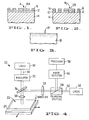
- FIG. 1 and 2 there is illustrated the typical steps associated with the fabrication of a semiconductor. More specifically, and as shown in Figure 1, a layer 12 of an oxide is deposited on a silicon substrate 14. The next step in the preparation of a semiconductor is to etch a pattern in the oxide through a lithographic and etching process. For example, a layer of photoresist material 16 is applied to the upper surface of the oxide. A mask is placed over the photoresist material and it is then exposed to light. The nonexposed portions are then removed to produce the structure that is illustrated in Figure 1. The thickness dimensions have been exaggerated for purposes of clarity.
- the latter structure is then "etched" in a step wherein portions of the oxide layer are removed in areas where the photoresist has been removed.
- a typical structure which is produced after the etching step is illustrated in Figure 2.
- Another technique used involves the principle of fluorescence.
- the photoresist is illuminated with U.V. radiation and the resultant fluoresence is observed.
- residues of the photoresist material can be detected.
- the fluorescent method similar to the standard visual inspection, the fluorescent method only gives gross indications of the success or failure of the removal or etching steps of the photoresist material.
- the fluorescent technique is applicable only to photoresist residues and not to the oxide or other residues.
- an ion beam is rastered over the surface of the sample.
- Some of the ions in the beam which bombard the sample are introduced into the lattice structure of the silicon.
- the concentration of the dopant ions in the sample is related to the length of time which the beam is focused on any point on the surface of the sample.
- the depth to which the ions penetrate is related to the voltage on the ion beam. However, even at maximum voltage, the depth to which the ions penetrate is relatively small such that the ion concentrations of interest are substantially at the upper surface of the sample.
- the ions which are incorporated into the surface of the silicon are located at interstitial sites and physically disrupt the lattice structure of the material. In this state, the material will not exhibit the desired semiconductive properties.
- the dopant is activated through an annealing process. In the annealing process, the material is heated in a manner to permit the lattice to reform, enabling the ions to move from the interstitial sites to substitutional sites. In this process, the dopant ions are substituted for silicon at various points in the lattice. This annealing step functions to remove defects in the lattice and free the electrons of the dopant ions for conduction of current.
- the dopant levels which have been implanted usually can be measured by known electrical resistivity methods.
- the doped silicon is now at least partially conductive, indications of the dopant characteristics can be obtained simply by measuring electrical parameters.
- the present electrical testing procedures are able to detect concentrations as low as 10 13 ions/cm 2 .
- concentrations as low as 10 ions/cm 2 .
- the prior art electrical technique has the additional shortcoming of being unable to detect ion concentrations prior to annealing.
- the electrons of the dopant ions in the sample are locked at interstitial sites in the lattice structure. Accordingly, no information can be obtained by electrical measurement techniques.
- such information can be invaluable in designing fabrication steps to improve and alter the characteristics of an integrated circuit.
- the subject invention provides for a new and improved method and apparatus for evaluating the surface conditions of a sample.
- the method and apparatus is based on the principle that the change in optical reflectivity of a sample as it is heated will be different, depending upon varying surface conditions. It has been known that optical reflectivity is dependent to some extent on temperature. This dependence is defined by the following equation:
- R o represents the reflectivity at a set temperature and the second term in the equation gives the change in reflectivity resulting from the change in the temperature of the sample surface.
- the term ( ⁇ R/ ⁇ T) is the temperature coefficient of reflectivity which represents the rate of change in reflectivity with respect to the change in temperature.
- the first term, R is at least four orders of magnitude greater than the second term for temperature changes ⁇ T of less than 100 degrees.
- the noise level associated with R o is on the order of ⁇ R 0 .
- the latter value is still 100 times greater than the second term of the equation which makes measurement of the second term quite difficult.
- the value of the ratio ( ⁇ R/ ⁇ T)( ⁇ T)/R 0 is on the order of 10 -4 to 10 -5 and therefore, has not been used as a measurement parameter.
- this difficulty is overcome by modulating the heating source. Periodic changes in reflectivity, which are occurring at the frequency of the modulation beam, are then monitored. This information can be processed by passing the signal through narrow bandwidth filters. The result is that the only periodic reflectivity signalLlR T , resulting from the periodic temperature variations ⁇ T is measured rather than the absolute reflectivity R T .
- the periodic reflectivity signal ⁇ R T is defined by the following equation: As seen from the above equation, the periodic reflectivity signal ⁇ R T is dependent on the temperature coefficient of reflectivity ( ⁇ R/ ⁇ T) times the periodic surface temperature ( ⁇ T). Where a surface layer is present, the relative effect of the latter two variables on the change in periodic reflectivity R is dependent, in part, upon the thickness of that surface layer. More specifically, where the residue layer (or perturbed surface layer) is less than 100 Angstroms thick, the effect on the periodic reflectivity signal ⁇ R T , due to the presence of the surface layer, is primarily a result of the change in the temperature coefficient of reflectivity ( ⁇ R/ ⁇ T). This is so because such a thin layer will have a neglible effect on the periodic surface temperature ⁇ T.
- the change in the temperature coefficient of reflectivity is measurable even for very thin layers.
- a change in the temperature coefficient of reflectivity can be measured when the layer of interest is as thin as 5 Angstroms. This sensitivity is based on the principle that a "clean" or undoped substrate will have a particular coefficient of reflectivity. The presence of dopants or a residue layer having a thickness as little as 5 Angstroms will nonetheless alter the temperature coefficient of reflectivity in a measurable manner.
- the ability to analyze such thin layers is based on the fact that reflection of an electromagnetic beam occurs right at the surface of the sample and any residues or dopants at or near the surface boundary will affect the temperature coefficient of reflectivity.
- the thermal parameters of the surface layer will also have an effect on the periodic reflectivity signal ART.
- the layer of interest will have thermal characteristics that are different from the underlying substrate. When this layer is extremely thin, the thermal characteristics are defined almost entirely by the underlying substrate. However, when the thickness of the layer of interest is increased, its effect on the thermal characteristics of the system will be evident through its effect on the periodic surface temperature ⁇ T.
- thermal waves where there is a periodic heat source, the changing surface temperatures are a result of and defined by underlying thermal waves.
- a discussion of the generation of thermal waves by focusing an intensity modulated heat source on a sample can be found in applicant's prior U.S. Patent No. 4,255,971, assigned to the same assignee as the subject invention and incorporated herein by reference.
- the relationship between the change in reflectivity and the generation of thermal waves provides an entirely new mechanism for measuring thermal waves in a sample.
- the measurement of thermal waves based on the change in reflectivity of a sample is disclosed incur copending European patent application no. representatives' reference no. 27123.
- the apparatus includes a means for generating localized periodic heating at the surface of the sample.
- a light probe is then directed onto the surface of the sample within the area which has been periodically heated.
- a means is provided for detecting the intensity variations of the probe beam which has been reflected from the surface.
- the sample is rastered relative to the heating and probe beams. Any changes in the output signal of the detector will indicate the presence of dopants or residues.
- the intensity variations measured can be compared to a known sample to evaluate the surface conditions.
- Another problem relates to the evaluation of ion dopant concentrations at the surface of the sample as illustrated in Figure 3.
- the subject invention provides a mechanism for solving both of these detection problems.
- FIG 4 there is illustrated the appratus 20 for carrying out the method of the subject invention.
- a substrate 22 is shown which may be an integrated circuit or any other sample which needs to be evaluated.
- Sample 22 is shown resting on a platform 24 capable of rastering the sample with respect to the detecting apparatus.
- Controllable stages are well known in the art and are also disclosed in U.S. Patent No. 4,255,971, cited above.
- the upper surface of the sample is subjected to a periodic localized heating.
- this periodic localized heating is provided by a laser 30 which is intensity modulated by modulator 32.
- the frequency of modulation is based on the electronics but is preferably greater than 50 kHz.
- the intensity modulated heating source could be supplied by electromagnetic radiation at various wavelengths, including X-rays, gamma rays, infrared, ultraviolet, visible light, microwaves or radio frequencies.
- the intensity modulated source can also be generated through thermal excitations arising from the interaction of the sample with an intensity modulated stream of particles, such as a beam of electrons, protons, neutrons, ions or molecules.
- an intensity modulated stream of particles such as a beam of electrons, protons, neutrons, ions or molecules.
- the intensity modulated beam 34 is then passed through a dichroic mirror 36 and is preferably focused on a sample by a microscopic objective 38.
- the heating beam is an argon ion laser and the dichroic mirror is transparent to argon ion radiation.
- the dichroic mirror functions to reflect the probe laser beam, which is preferably generated by a helium-neon laser.
- the periodic heating source disclosed above is identical to the type used in various thermal wave generation systems.
- the intensity modulated beam will function to generate thermal waves in the sample.
- information about the thermal conductivity of the uppermost layers of the sample can be determined by an analysis of the thermal waves generated in the sample.
- the reflectivity signal will be affected by the thermal parameters of the sample as set forth in equation (2).
- a component of the reflectivity signal ⁇ R T will represent the thermal characteristics of the layer. In that case, information about the layer may be determined by an analysis of the thermal waves.
- the layer of interest When the layer of interest is relatively thin, its thermal characteristics will not measurably affect the thermal parameters of the sample and thus will not measurably change the periodic surface temperature ⁇ T. However, if the layer is at least 5 Angstroms thick, the layer will still alter the temperature coefficient of reflectivity (bR/JT) of the sample. The latter phenomenon is taken advantage of in the subject invention to permit the evaluation of extremely thin layers due to the change in the temperature coefficient of reflectivity.
- the detection means is defined by a light probe which is directed onto the surface of the sample that has been periodically heated by the modulated energy beam 34.
- the light probe is generated by a helium-neon laser 50.
- Various other sources of electromagnetic radiation may be used for the probe beam as long as the beam reflectivity is affected by the temperature changes on the sample surface in a manner which can be measured.
- the probe beam 52 emanating from the helium-neon laser 50 is then passed through a polarizing splitter 54.
- the polarizing splitter is oriented in such a manner as to let the coherent light emanating from laser 50 to pass freely therethrough. The splitter will, however, deflect all light whose phase has been rotated through 90° relative to beam 52. The reason for this arrangement will become apparent below.
- Waveplate 55 functions to rotate the phase of the beam by 45°.
- the waveplate will rotate the phase of the beam another 45° so that when it reaches splitter 54, the phase of the beam has been rotated a total of 90° from the incoming orientation.
- the splitter 54 will deflect the retro-reflected light beam up to detector 56, as discussed in more detail below.
- the probe beam 52 After the probe beam 52 initially passes through the waveplate, it is reflected downwardly by dichroic mirror 36.
- the dichroic mirror is transparent to argon ion light but will reflect the light rays in the helium-neon frequencies.
- the heating beam and the probe beam are aligned in a manner such that they are directed in a coincident manner down through lens 38 and focused at the same spot on the surface of the sample. By focusing the probe beam and the heating beam at the same spot, the maximum signal output can be achieved.
- the reflectivity signals of interest exist at any area on the surface of the sample which has been periodically heated by the beam 34. Therefore, the probe beam would not have to be directly coincident with the heating beam to detect the signals of interest. Accordingly, a microscope objective 38 is not necessary for focusing either the heating beam 34 or the probe beam 52. Rather, it is only necessary to direct the probe beam within at least a portion of the periodically heated area.
- a discussion and equations for calculating the size of the periodically heated area are set forth in copending application Serial No. 401,511, assigned to the same assignee as the subject application and incorporated herein by reference. Briefly, the diameter of the heated area, extending radially away from the center of the heating beam, is a function of the diameter and frequency of the heating beam and the thermal parameters in the sample.
- the optical lens system should be capable of focusing the incoming heating and probe beams to a spot size of 1 micron in diameter.
- the probe beam 52 impinges on the surface of the sample and interacts with the electrons and thus with the lattice structure of the sample.
- the lattice structure of the sample will undergo periodic changes as the temperature of the sample changes periodically.
- the probe beam essentially "sees” the changes in this lattice structure and the level of reflectivity of the beam changes along with the changing thermal conditions of the sample surface.
- the probe beam is reflected back up to the dichroic mirror where it is, in turn, reflected back along the incoming beam path through the 1/4A-waveplate 55.
- waveplate 55 rotates the phase of the probe beam by another 45° such that when the beam reaches splitter 54, its phase has been rotated 90° with respect to the original beam.
- the splitter will deflect the retro-reflected probe beam upwardly towards detector 56. Since intensity variations of the probe beam are to be detected, a standard photodetector may be employed as a sensing mechanism. The intensity variations which are measured are then supplied as an output signal to a processor 58 for evaluating the surface conditions of the sample.
- processor 58 The operation of processor 58 is dependent on the type of testing configuration which is utilized. In all cases, however, the processor is designed to evaluate the periodic intensity changes of the incoming probe beam which are the result of the reflectivity changes caused by the periodic heating on the sample. These high frequency changes are filtered to produce a signal which may be evaluated.
- the processor may be programmed with the value of a known signal, for example, an uncoated or untreated oxide. If residues are present, as for example, as shown in hole HI of Figure 1, the output signal measured will be different from the known, stored signal, indicating the presence of residues. Because the identity of a particular residue is rarely known, an evaluation of the thickness of residue layer would be quite difficult. However, in most manufacturing situations, only the detection of the presence of the residue is necessary.
- a sample could be rastered with respect to the heating and probe beams.
- the movements of platform 24 can be programmed in a manner to trace the paths defined by the etched tracks as shown in Figure 2. If no residues remain, the output signal should remain constant. In contrast, any peaks or variations in the output signal will indicate the presence of residues.
- ion implanted dopants With ion implanted dopants more quantitative information can be obtained because the identity, and thus the thermal characteristics, of both the substrate and the dopant are known. For example, the output signals can be normalized against a known reference sample such that actual concentrations of the implanted dopants may be obtained. As discussed above, this system is capable of detecting dopant levels prior to the annealing process. Unlike electrical testing, which requires the dopant to be activated, the ions locked at the interstitial sites, prior to annealing, will nonetheless affect the temperature coefficient of reflectivity and therefore can be monitored.
- the subject invention has been shown to be capable of detecting boron ion dopant concentrations in silicon as low as 10 ions/cm 2 .
- This sensitivity is three orders of magnitude greater than the electrical testing available in the prior art.
- Analysis can also be performed by rastering the sample relative to the heating and probe beams to generate one or two dimensional maps of dopant concentrations.
- a means for generating a localized periodic heating at the surface of the sample.
- the heating means is an intensity modulated laser.
- the detection system further includes a probe beam which is focused on the area periodically heated by the intensity modulated laser in a manner to reflect off the surface of the sample.
- a means is provided for detecting the intensity variations of the reflected light resulting from the periodic heating. By processing the measured intensity variations of the reflected beam, surface conditions of the sample can be evaluated.
Landscapes
- Physics & Mathematics (AREA)
- Health & Medical Sciences (AREA)
- Life Sciences & Earth Sciences (AREA)
- Chemical & Material Sciences (AREA)
- Analytical Chemistry (AREA)
- Biochemistry (AREA)
- General Health & Medical Sciences (AREA)
- General Physics & Mathematics (AREA)
- Immunology (AREA)
- Pathology (AREA)
- Investigating Or Analysing Materials By Optical Means (AREA)
- Testing Or Measuring Of Semiconductors Or The Like (AREA)
- Investigating Or Analyzing Materials Using Thermal Means (AREA)
Applications Claiming Priority (2)
| Application Number | Priority Date | Filing Date | Title |
|---|---|---|---|
| US612076 | 1984-05-21 | ||
| US06/612,076 US4636088A (en) | 1984-05-21 | 1984-05-21 | Method and apparatus for evaluating surface conditions of a sample |
Publications (3)
| Publication Number | Publication Date |
|---|---|
| EP0162681A2 true EP0162681A2 (de) | 1985-11-27 |
| EP0162681A3 EP0162681A3 (en) | 1987-06-16 |
| EP0162681B1 EP0162681B1 (de) | 1990-07-25 |
Family
ID=24451619
Family Applications (1)
| Application Number | Title | Priority Date | Filing Date |
|---|---|---|---|
| EP85303509A Expired EP0162681B1 (de) | 1984-05-21 | 1985-05-20 | Verfahren und Vorrichtung zur Untersuchung der Oberflächenbedingungen einer Probe |
Country Status (4)
| Country | Link |
|---|---|
| US (1) | US4636088A (de) |
| EP (1) | EP0162681B1 (de) |
| JP (1) | JPS60256031A (de) |
| DE (1) | DE3578824D1 (de) |
Cited By (8)
| Publication number | Priority date | Publication date | Assignee | Title |
|---|---|---|---|---|
| EP0211590A2 (de) * | 1985-08-02 | 1987-02-25 | AT&T Corp. | Verfahren und Vorrichtung zur optischen Fehlerbestimmung in einem Halbleitermaterial |
| EP0239408A2 (de) * | 1986-03-28 | 1987-09-30 | Therma-Wave Inc. | Verfahren und Vorrichtung zur optischen Erfassung von Oberflächenzuständen in Stoffen |
| EP0291276A2 (de) * | 1987-05-15 | 1988-11-17 | Therma-Wave Inc. | Ortung und Prüfung von in Betracht kommenden Flächen auf einem Werkstück |
| EP0432963A2 (de) * | 1989-12-12 | 1991-06-19 | THERMA-WAVE, INC. (a Delaware corporation) | Verfahren und Gerät zum Einschätzen der Ioneneinpflanzungsdosierungshöhen und Halbleitern |
| DE4035266A1 (de) * | 1990-11-02 | 1992-05-07 | Jenoptik Jena Gmbh | Verfahren und anordnung zur thermowellenanalyse |
| DE19819144C1 (de) * | 1998-04-29 | 2000-06-15 | Tga Tech Geraete Und Apparateb | Verfahren zur mikroskopischen Untersuchung der Gewebeintegration von Festkörpern, die dauerhaft oder vorübergehend in lebende Organismen implantiert werden und Vorrichtung zur Durchführung des Verfahrens |
| FR2839154A1 (fr) * | 2002-04-30 | 2003-10-31 | Nat Inst Of Advanced Ind Scien | Procede et systeme de mesure d'une courte reponse temporelle a l'aide d'une courte impulsion |
| US7395211B2 (en) | 2000-08-16 | 2008-07-01 | Dolby Laboratories Licensing Corporation | Modulating one or more parameters of an audio or video perceptual coding system in response to supplemental information |
Families Citing this family (73)
| Publication number | Priority date | Publication date | Assignee | Title |
|---|---|---|---|---|
| US4952063A (en) * | 1985-03-01 | 1990-08-28 | Therma-Wave, Inc. | Method and apparatus for evaluating surface and subsurface features in a semiconductor |
| EP0200301A1 (de) * | 1985-03-01 | 1986-11-05 | Therma-Wave Inc. | Verfahren und Vorrichtung zum Auswerten von Eigenschaften der Oberfläche und des Inneren eines Halbleiters |
| US4927766A (en) * | 1986-05-27 | 1990-05-22 | The Boc Group, Inc. | Gas constituent measurement and recording |
| US4921348A (en) * | 1989-01-26 | 1990-05-01 | Iowa State University Research Foundation, Inc. | Method and means for a spatial and temporal probe for laser-generated plumes based on density gradients |
| US5136172A (en) * | 1989-08-16 | 1992-08-04 | Hitachi, Ltd. | Method and apparatus for detecting photoacoustic signal |
| DD291157A5 (de) * | 1989-12-28 | 1991-06-20 | ����@�����@�����@����k�� | Anordnung zur thermowellenanalyse von schichtsystemen |
| US5221142A (en) * | 1991-05-20 | 1993-06-22 | Peak Systems, Inc. | Method and apparatus for temperature measurement using thermal expansion |
| US5479259A (en) * | 1991-05-20 | 1995-12-26 | Hitachi, Ltd. | Method and apparatus for detecting photoacoustic signal |
| US5258612A (en) * | 1992-04-01 | 1993-11-02 | Clark William G | Timed-resolved spectroscopy with split pump and probe pulses |
| JPH05277075A (ja) * | 1992-04-03 | 1993-10-26 | Topcon Corp | 眼軸長測定装置 |
| US5406378A (en) * | 1992-04-29 | 1995-04-11 | Mpb Technologies Inc. | Method and apparatus for non-contact and rapid identification of wood species |
| US5229304A (en) * | 1992-05-04 | 1993-07-20 | At&T Bell Laboratories | Method for manufacturing a semiconductor device, including optical inspection |
| US5228776A (en) * | 1992-05-06 | 1993-07-20 | Therma-Wave, Inc. | Apparatus for evaluating thermal and electrical characteristics in a sample |
| DE4223337C2 (de) * | 1992-07-16 | 1996-02-22 | Jenoptik Jena Gmbh | Verfahren und Anordnung zur photothermischen Spektroskopie |
| US5638396A (en) * | 1994-09-19 | 1997-06-10 | Textron Systems Corporation | Laser ultrasonics-based material analysis system and method |
| US5574562A (en) * | 1994-12-19 | 1996-11-12 | The Board Of Trustees Of The Leland Stanford Junior University | Method and apparatus for evaluation of high temperature superconductors |
| US5657754A (en) * | 1995-07-10 | 1997-08-19 | Rosencwaig; Allan | Apparatus for non-invasive analyses of biological compounds |
| US6008906A (en) | 1995-08-25 | 1999-12-28 | Brown University Research Foundation | Optical method for the characterization of the electrical properties of semiconductors and insulating films |
| US5706094A (en) * | 1995-08-25 | 1998-01-06 | Brown University Research Foundation | Ultrafast optical technique for the characterization of altered materials |
| US6321601B1 (en) | 1996-08-06 | 2001-11-27 | Brown University Research Foundation | Optical method for the characterization of laterally-patterned samples in integrated circuits |
| US6175416B1 (en) | 1996-08-06 | 2001-01-16 | Brown University Research Foundation | Optical stress generator and detector |
| US5748318A (en) * | 1996-01-23 | 1998-05-05 | Brown University Research Foundation | Optical stress generator and detector |
| US6095679A (en) * | 1996-04-22 | 2000-08-01 | Ta Instruments | Method and apparatus for performing localized thermal analysis and sub-surface imaging by scanning thermal microscopy |
| US5844684A (en) * | 1997-02-28 | 1998-12-01 | Brown University Research Foundation | Optical method for determining the mechanical properties of a material |
| US5748317A (en) * | 1997-01-21 | 1998-05-05 | Brown University Research Foundation | Apparatus and method for characterizing thin film and interfaces using an optical heat generator and detector |
| US5978074A (en) | 1997-07-03 | 1999-11-02 | Therma-Wave, Inc. | Apparatus for evaluating metalized layers on semiconductors |
| US5864393A (en) * | 1997-07-30 | 1999-01-26 | Brown University Research Foundation | Optical method for the determination of stress in thin films |
| US6108087A (en) * | 1998-02-24 | 2000-08-22 | Kla-Tencor Corporation | Non-contact system for measuring film thickness |
| US6552803B1 (en) | 1998-02-24 | 2003-04-22 | Kla-Tencor Corporation | Detection of film thickness through induced acoustic pulse-echos |
| US6049220A (en) * | 1998-06-10 | 2000-04-11 | Boxer Cross Incorporated | Apparatus and method for evaluating a wafer of semiconductor material |
| US6885444B2 (en) * | 1998-06-10 | 2005-04-26 | Boxer Cross Inc | Evaluating a multi-layered structure for voids |
| US6054868A (en) * | 1998-06-10 | 2000-04-25 | Boxer Cross Incorporated | Apparatus and method for measuring a property of a layer in a multilayered structure |
| US7612890B2 (en) * | 1998-06-30 | 2009-11-03 | Lockheed Martin Corporation | System and method for controlling wafer temperature |
| US6025918A (en) * | 1998-07-07 | 2000-02-15 | Brown University Research Foundation | Apparatus and method for measurement of the mechanical properties and electromigration of thin films |
| US6038026A (en) | 1998-07-07 | 2000-03-14 | Brown University Research Foundation | Apparatus and method for the determination of grain size in thin films |
| US6323951B1 (en) | 1999-03-22 | 2001-11-27 | Boxer Cross Incorporated | Apparatus and method for determining the active dopant profile in a semiconductor wafer |
| DE19927760A1 (de) * | 1999-06-17 | 2000-12-21 | Daimler Chrysler Ag | Vorrichtung und Verfahren zur thermographischen Untersuchung von Funktionsflächen an Umformwerkzeugen |
| US6654488B1 (en) * | 1999-07-01 | 2003-11-25 | International Business Machines Corporation | Fill pattern inspection |
| US6317216B1 (en) | 1999-12-13 | 2001-11-13 | Brown University Research Foundation | Optical method for the determination of grain orientation in films |
| US6535285B1 (en) | 2000-02-08 | 2003-03-18 | Therma-Wave, Inc. | Combination thermal wave and optical spectroscopy measurement system |
| US6812047B1 (en) * | 2000-03-08 | 2004-11-02 | Boxer Cross, Inc. | Evaluating a geometric or material property of a multilayered structure |
| US6408048B2 (en) | 2000-03-14 | 2002-06-18 | Therma-Wave, Inc. | Apparatus for analyzing samples using combined thermal wave and X-ray reflectance measurements |
| US6532070B1 (en) | 2000-07-17 | 2003-03-11 | Therma-Wave, Inc. | Method for determining ion concentration and energy of shallow junction implants |
| US6696692B1 (en) * | 2000-11-06 | 2004-02-24 | Hrl Laboratories, Llc | Process control methods for use with e-beam fabrication technology |
| US6911349B2 (en) * | 2001-02-16 | 2005-06-28 | Boxer Cross Inc. | Evaluating sidewall coverage in a semiconductor wafer |
| US6812717B2 (en) * | 2001-03-05 | 2004-11-02 | Boxer Cross, Inc | Use of a coefficient of a power curve to evaluate a semiconductor wafer |
| US6940592B2 (en) * | 2001-10-09 | 2005-09-06 | Applied Materials, Inc. | Calibration as well as measurement on the same workpiece during fabrication |
| US6971791B2 (en) * | 2002-03-01 | 2005-12-06 | Boxer Cross, Inc | Identifying defects in a conductive structure of a wafer, based on heat transfer therethrough |
| US6958814B2 (en) * | 2002-03-01 | 2005-10-25 | Applied Materials, Inc. | Apparatus and method for measuring a property of a layer in a multilayered structure |
| US6989899B2 (en) * | 2002-03-18 | 2006-01-24 | Therma-Wave, Inc. | Ion implant monitoring through measurement of modulated optical response |
| US7106446B2 (en) * | 2002-06-21 | 2006-09-12 | Therma-Wave, Inc. | Modulated reflectance measurement system with multiple wavelengths |
| EP1391708B1 (de) * | 2002-08-14 | 2007-12-26 | Sony Deutschland GmbH | Verfahren zur Bestimmung der Temperatur eines Systems |
| US6963393B2 (en) * | 2002-09-23 | 2005-11-08 | Applied Materials, Inc. | Measurement of lateral diffusion of diffused layers |
| US7126690B2 (en) * | 2002-09-23 | 2006-10-24 | Therma-Wave, Inc. | Modulated reflectance measurement system using UV probe |
| US6878559B2 (en) * | 2002-09-23 | 2005-04-12 | Applied Materials, Inc. | Measurement of lateral diffusion of diffused layers |
| KR100512005B1 (ko) * | 2002-11-28 | 2005-09-02 | 삼성전자주식회사 | 이온주입된 웨이퍼의 오염 탐지 방법 및 장치 |
| US6950190B2 (en) * | 2003-01-09 | 2005-09-27 | Therma-Wave, Inc. | Scatterometry for junction metrology |
| US6888632B2 (en) * | 2003-02-28 | 2005-05-03 | Therma-Wave, Inc. | Modulated scatterometry |
| US6952261B2 (en) * | 2003-03-31 | 2005-10-04 | Therma-Wave, Inc. | System for performing ellipsometry using an auxiliary pump beam to reduce effective measurement spot size |
| US7248367B2 (en) * | 2003-06-10 | 2007-07-24 | Therma-Wave, Inc. | Characterization of ultra shallow junctions in semiconductor wafers |
| US20040253751A1 (en) * | 2003-06-16 | 2004-12-16 | Alex Salnik | Photothermal ultra-shallow junction monitoring system with UV pump |
| US7212288B2 (en) * | 2003-08-14 | 2007-05-01 | Therma-Wave, Inc. | Position modulated optical reflectance measurement system for semiconductor metrology |
| US7280215B2 (en) * | 2003-09-24 | 2007-10-09 | Therma-Wave, Inc. | Photothermal system with spectroscopic pump and probe |
| US7045798B2 (en) * | 2004-02-20 | 2006-05-16 | Applied Materials, Inc. | Characterizing an electron beam treatment apparatus |
| US7026175B2 (en) * | 2004-03-29 | 2006-04-11 | Applied Materials, Inc. | High throughput measurement of via defects in interconnects |
| WO2006002150A1 (en) * | 2004-06-22 | 2006-01-05 | Applied Materials Israel, Ltd. | Wafer inspection system |
| US7379185B2 (en) | 2004-11-01 | 2008-05-27 | Applied Materials, Inc. | Evaluation of openings in a dielectric layer |
| GB0427318D0 (en) * | 2004-12-14 | 2005-01-19 | Imec Inter Uni Micro Electr | Method and device for the independent extraction of carrier concentration level and electrical junction depth in a semiconductor substrate |
| US7499168B2 (en) * | 2006-02-14 | 2009-03-03 | Kla-Tencor Corp. | Combined modulated optical reflectance and electrical system for ultra-shallow junctions applications |
| US7502104B2 (en) * | 2006-08-10 | 2009-03-10 | Kla-Tencor Corporation | Probe beam profile modulated optical reflectance system and methods |
| US20080318345A1 (en) * | 2007-06-22 | 2008-12-25 | Persing Harold M | Plasma ion implantation process control using reflectometry |
| HUE026962T2 (en) * | 2009-03-17 | 2016-07-28 | Imec | A method for determining the transient depth of a semiconductor area |
| TW202136743A (zh) * | 2019-12-05 | 2021-10-01 | 加拿大商奧羅拉太陽能科技加拿大公司 | 對半導體材料進行特性分析之系統和方法 |
Citations (1)
| Publication number | Priority date | Publication date | Assignee | Title |
|---|---|---|---|---|
| US4243327A (en) * | 1979-01-31 | 1981-01-06 | Nasa | Double-beam optical method and apparatus for measuring thermal diffusivity and other molecular dynamic processes in utilizing the transient thermal lens effect |
Family Cites Families (9)
| Publication number | Priority date | Publication date | Assignee | Title |
|---|---|---|---|---|
| US3462602A (en) * | 1967-08-16 | 1969-08-19 | Automation Ind Inc | Infra-red flaw detector |
| FR2198636A5 (de) * | 1972-09-06 | 1974-03-29 | France Etat | |
| US4255971A (en) * | 1978-11-01 | 1981-03-17 | Allan Rosencwaig | Thermoacoustic microscopy |
| JPS567006A (en) * | 1979-06-22 | 1981-01-24 | Ibm | Method of extending measurement range of interference |
| US4455741A (en) * | 1982-02-11 | 1984-06-26 | At&T Bell Laboratories | Fabrication of solid state electronic devices using fluorescent imaging of surface temperature profiles |
| US4468136A (en) * | 1982-02-12 | 1984-08-28 | The Johns Hopkins University | Optical beam deflection thermal imaging |
| US4446719A (en) * | 1982-07-22 | 1984-05-08 | General Motors Corporation | Electroreflectance vibrational spectroscopy |
| US4521118A (en) * | 1982-07-26 | 1985-06-04 | Therma-Wave, Inc. | Method for detection of thermal waves with a laser probe |
| US4579463A (en) * | 1984-05-21 | 1986-04-01 | Therma-Wave Partners | Detecting thermal waves to evaluate thermal parameters |
-
1984
- 1984-05-21 US US06/612,076 patent/US4636088A/en not_active Expired - Lifetime
-
1985
- 1985-05-17 JP JP60105732A patent/JPS60256031A/ja active Granted
- 1985-05-20 DE DE8585303509T patent/DE3578824D1/de not_active Expired - Lifetime
- 1985-05-20 EP EP85303509A patent/EP0162681B1/de not_active Expired
Patent Citations (1)
| Publication number | Priority date | Publication date | Assignee | Title |
|---|---|---|---|---|
| US4243327A (en) * | 1979-01-31 | 1981-01-06 | Nasa | Double-beam optical method and apparatus for measuring thermal diffusivity and other molecular dynamic processes in utilizing the transient thermal lens effect |
Non-Patent Citations (3)
| Title |
|---|
| APPLIED OPTICS, vol. 22, no. 20, October 1983, pages 3169-3176, New York, US; J. OPSAL et al.: "Thermal-wave detection and thin-film thickness measurements with laser beam deflection" * |
| IEEE TRANSACTIONS ON SONIDS AND ULTRASONICS, vol. SU-32, no. 2, March 1985, pages 365-373, New York, US; C.C. WILLIAMS "High-resolution photothermal laser probe" * |
| LASER FOCUS, vol. 16, no. 6, June 1980, page 42, Newton, US; "Yag-laser inspection of solder joints would speed processing of pc boards" * |
Cited By (12)
| Publication number | Priority date | Publication date | Assignee | Title |
|---|---|---|---|---|
| EP0211590A2 (de) * | 1985-08-02 | 1987-02-25 | AT&T Corp. | Verfahren und Vorrichtung zur optischen Fehlerbestimmung in einem Halbleitermaterial |
| EP0211590A3 (en) * | 1985-08-02 | 1988-04-20 | American Telephone And Telegraph Company | Method and apparatus for optically determining defects in a semiconductor material |
| EP0239408A2 (de) * | 1986-03-28 | 1987-09-30 | Therma-Wave Inc. | Verfahren und Vorrichtung zur optischen Erfassung von Oberflächenzuständen in Stoffen |
| EP0239408A3 (de) * | 1986-03-28 | 1989-06-21 | Therma-Wave Inc. | Verfahren und Vorrichtung zur optischen Erfassung von Oberflächenzuständen in Stoffen |
| EP0291276A2 (de) * | 1987-05-15 | 1988-11-17 | Therma-Wave Inc. | Ortung und Prüfung von in Betracht kommenden Flächen auf einem Werkstück |
| EP0291276A3 (en) * | 1987-05-15 | 1990-05-30 | Therma-Wave Inc. | Locating and testing areas of interest on a workpiece |
| EP0432963A2 (de) * | 1989-12-12 | 1991-06-19 | THERMA-WAVE, INC. (a Delaware corporation) | Verfahren und Gerät zum Einschätzen der Ioneneinpflanzungsdosierungshöhen und Halbleitern |
| EP0432963A3 (en) * | 1989-12-12 | 1992-06-03 | Therma-Wave Inc. | Method and apparatus for evaluating ion implant dosage levels in semiconductors |
| DE4035266A1 (de) * | 1990-11-02 | 1992-05-07 | Jenoptik Jena Gmbh | Verfahren und anordnung zur thermowellenanalyse |
| DE19819144C1 (de) * | 1998-04-29 | 2000-06-15 | Tga Tech Geraete Und Apparateb | Verfahren zur mikroskopischen Untersuchung der Gewebeintegration von Festkörpern, die dauerhaft oder vorübergehend in lebende Organismen implantiert werden und Vorrichtung zur Durchführung des Verfahrens |
| US7395211B2 (en) | 2000-08-16 | 2008-07-01 | Dolby Laboratories Licensing Corporation | Modulating one or more parameters of an audio or video perceptual coding system in response to supplemental information |
| FR2839154A1 (fr) * | 2002-04-30 | 2003-10-31 | Nat Inst Of Advanced Ind Scien | Procede et systeme de mesure d'une courte reponse temporelle a l'aide d'une courte impulsion |
Also Published As
| Publication number | Publication date |
|---|---|
| JPH0347704B2 (de) | 1991-07-22 |
| DE3578824D1 (de) | 1990-08-30 |
| US4636088A (en) | 1987-01-13 |
| JPS60256031A (ja) | 1985-12-17 |
| EP0162681B1 (de) | 1990-07-25 |
| EP0162681A3 (en) | 1987-06-16 |
Similar Documents
| Publication | Publication Date | Title |
|---|---|---|
| EP0162681A2 (de) | Verfahren und Vorrichtung zur Untersuchung der Oberflächenbedingungen einer Probe | |
| US5228776A (en) | Apparatus for evaluating thermal and electrical characteristics in a sample | |
| EP0200301A1 (de) | Verfahren und Vorrichtung zum Auswerten von Eigenschaften der Oberfläche und des Inneren eines Halbleiters | |
| EP0163466B1 (de) | Verfahren und Vorrichtung zur Messung der Dicke und Zusammensetzungen einer geschichteten oder dünnschichtigen Probe | |
| US6483594B2 (en) | Apparatus and method for determining the active dopant profile in a semiconductor wafer | |
| US6052185A (en) | Method and apparatus for measuring the concentration of ions implanted in semiconductor materials | |
| US4579463A (en) | Detecting thermal waves to evaluate thermal parameters | |
| EP0615123B1 (de) | Methode und vorrichtung zur oberflächenanalyse | |
| JP5009506B2 (ja) | 試料の1つ又は複数の特性を決定するための方法とシステム | |
| US7589834B2 (en) | Detection method and apparatus metal particulates on semiconductors | |
| JP2002540396A5 (de) | ||
| KR20020070424A (ko) | 미세 전자 형태의 품질 특성화 방법 및 장치 | |
| WO2001088955A2 (en) | Method of monitoring ion implants by examination of an overlying masking material | |
| EP1118005A4 (de) | Verfahren und vorrichtung zur auswertung von halbleiterscheiben | |
| JP4783801B2 (ja) | 非振動式接触電位差センサおよび制御された照射を利用した半導体検査システムおよび装置 | |
| US6760100B2 (en) | Method and apparatus for classifying defects occurring at or near a surface of a smooth substrate | |
| JP5239346B2 (ja) | ラマン分光を用いた応力評価方法及び半導体装置の製造方法 | |
| US20060166385A1 (en) | Method for measuring peak carrier concentration in ultra-shallow junctions | |
| US7816152B2 (en) | In situ, ex situ and inline process monitoring, optimization and fabrication | |
| US6573498B1 (en) | Electric measurement of reference sample in a CD-SEM and method for calibration | |
| US6825933B2 (en) | Computer-implemented reflectance system and method for non-destructive low dose ion implantation monitoring | |
| US4777146A (en) | Fabrication process involving semi-insulating material | |
| JPH07294460A (ja) | X線分析方法および装置 | |
| JPH10154734A (ja) | 半導体結晶の評価方法 | |
| JPH0521566A (ja) | 半導体結晶におけるイオン注入量測定方法 |
Legal Events
| Date | Code | Title | Description |
|---|---|---|---|
| PUAI | Public reference made under article 153(3) epc to a published international application that has entered the european phase |
Free format text: ORIGINAL CODE: 0009012 |
|
| AK | Designated contracting states |
Designated state(s): DE FR GB NL |
|
| PUAL | Search report despatched |
Free format text: ORIGINAL CODE: 0009013 |
|
| AK | Designated contracting states |
Kind code of ref document: A3 Designated state(s): DE FR GB NL |
|
| 17P | Request for examination filed |
Effective date: 19871208 |
|
| 17Q | First examination report despatched |
Effective date: 19890307 |
|
| GRAA | (expected) grant |
Free format text: ORIGINAL CODE: 0009210 |
|
| AK | Designated contracting states |
Kind code of ref document: B1 Designated state(s): DE FR GB NL |
|
| REF | Corresponds to: |
Ref document number: 3578824 Country of ref document: DE Date of ref document: 19900830 |
|
| ET | Fr: translation filed | ||
| PLBE | No opposition filed within time limit |
Free format text: ORIGINAL CODE: 0009261 |
|
| STAA | Information on the status of an ep patent application or granted ep patent |
Free format text: STATUS: NO OPPOSITION FILED WITHIN TIME LIMIT |
|
| 26N | No opposition filed | ||
| NLS | Nl: assignments of ep-patents |
Owner name: THERMA-WAVE, INC., (DELAWARE) TE FREMONT, CALIFORN |
|
| REG | Reference to a national code |
Ref country code: FR Ref legal event code: TP |
|
| REG | Reference to a national code |
Ref country code: GB Ref legal event code: 732E |
|
| REG | Reference to a national code |
Ref country code: GB Ref legal event code: IF02 |
|
| PGFP | Annual fee paid to national office [announced via postgrant information from national office to epo] |
Ref country code: GB Payment date: 20020515 Year of fee payment: 18 |
|
| PGFP | Annual fee paid to national office [announced via postgrant information from national office to epo] |
Ref country code: FR Payment date: 20020527 Year of fee payment: 18 |
|
| PGFP | Annual fee paid to national office [announced via postgrant information from national office to epo] |
Ref country code: NL Payment date: 20020529 Year of fee payment: 18 Ref country code: DE Payment date: 20020529 Year of fee payment: 18 |
|
| PG25 | Lapsed in a contracting state [announced via postgrant information from national office to epo] |
Ref country code: GB Free format text: LAPSE BECAUSE OF NON-PAYMENT OF DUE FEES Effective date: 20030520 |
|
| PG25 | Lapsed in a contracting state [announced via postgrant information from national office to epo] |
Ref country code: NL Free format text: LAPSE BECAUSE OF NON-PAYMENT OF DUE FEES Effective date: 20031201 |
|
| PG25 | Lapsed in a contracting state [announced via postgrant information from national office to epo] |
Ref country code: DE Free format text: LAPSE BECAUSE OF NON-PAYMENT OF DUE FEES Effective date: 20031202 |
|
| GBPC | Gb: european patent ceased through non-payment of renewal fee |
Effective date: 20030520 |
|
| PG25 | Lapsed in a contracting state [announced via postgrant information from national office to epo] |
Ref country code: FR Free format text: LAPSE BECAUSE OF NON-PAYMENT OF DUE FEES Effective date: 20040130 |
|
| NLV4 | Nl: lapsed or anulled due to non-payment of the annual fee |
Effective date: 20031201 |
|
| REG | Reference to a national code |
Ref country code: FR Ref legal event code: ST |
|
| P01 | Opt-out of the competence of the unified patent court (upc) registered |
Effective date: 20230525 |