EP0160426A2 - Datenhalteschaltung - Google Patents
Datenhalteschaltung Download PDFInfo
- Publication number
- EP0160426A2 EP0160426A2 EP85302439A EP85302439A EP0160426A2 EP 0160426 A2 EP0160426 A2 EP 0160426A2 EP 85302439 A EP85302439 A EP 85302439A EP 85302439 A EP85302439 A EP 85302439A EP 0160426 A2 EP0160426 A2 EP 0160426A2
- Authority
- EP
- European Patent Office
- Prior art keywords
- film
- layer
- layers
- memory according
- adjacent
- Prior art date
- Legal status (The legal status is an assumption and is not a legal conclusion. Google has not performed a legal analysis and makes no representation as to the accuracy of the status listed.)
- Withdrawn
Links
Images

Classifications
-
- G—PHYSICS
- G11—INFORMATION STORAGE
- G11C—STATIC STORES
- G11C21/00—Digital stores in which the information circulates continuously
-
- G—PHYSICS
- G11—INFORMATION STORAGE
- G11C—STATIC STORES
- G11C21/00—Digital stores in which the information circulates continuously
- G11C21/005—Digital stores in which the information circulates continuously using electrical delay lines
Definitions
- This invention relates to an information holding device.
- the device is referred to below as a memory, though it is to be understood that the information may be held only briefly, in which case the device may function, for example, as a delay line, or the information may be held for a longer time, in which case the device may function as a normal memory.
- EP 0077135A and copending European Patent Application No. 84301981.1 describe memories employing a film comprising a plurality of monomolecular layers.
- the film is described as being formed by the Langmuir-Blodgett technique, and in the case of the European Patent Application at least one of the layers is formed by a process of chemisorption.
- each layer is capable of carrying a charge.
- a charge injector is located on one side of the film for introducing charges into the film in a time sequence which corresponds to the information to be carried. Means are provided for applying a voltage between the faces of the film to cause the charge carried by any larger to be transferred to the adjacent layer.
- the sequence of charges carried by the film may be read out by a photon-emitting electron arrival detector or by a method of current differentiation.
- At least some of the layers of the film are preferably formed of a polydiacetylene (PDA), though other materials may be used, for example a porphyrin.
- PDA polydiacetylene
- the charge injector described in the above mentioned specification and application takes the form of a photo- injector layer which injects charge into the adjacent film layer in response to incident photons.
- the present invention provides a memory of the same type as that described in the above-mentioned European specification and application (the disclosures of which are incorporated herein by reference) but with a charge injector which does not require a source of photons.
- a memory for carrying information comprising a multilayer film comprising a plurality of monomolecular layers and in which each layer is capable of carrying a charge; means for introducing charges into one side of the film in a time sequence which corresponds to the information to be carried; means for applying a voltage between the faces of the film to cause the charge carried by any layer to be transferred to the adjacent layer; and means for reading out the sequence of charges carried by the film; wherein the charge introducing means comprises electrodes adjacent opposite faces of the film and means for applying across the film voltage pulses of an amplitude greater than that required to cause tunnelling without thermal activation between the layers of the film and at least equal to that required to cause electrons to tunnel without thermal activation from one of the electrodes to the film layer adjacent thereto.
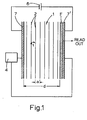
- the embodiment shown in Figure 1 comprises a film 1 formed of a plurality of n monomolecular layers 2 (eight are illustrated).
- the layers are alternately of different materials to enable a charge pattern injected into the layers to be frozen therein.
- EP 0077135A discloses a memory wherein the film is composed of layers of at least two materials having different electron affinities, at least one of the materials being sandwiched between adjacent layers, or groups of layers, of the other of the materials.
- the layers are spaced a distance a apart from one another and the overall film thickness is d.
- Adjacent opposite faces of the film 1 are electrodes 7 and 7' via which a d.c.
- the electrodes also enable a voltage pulse train, the pulses of which represent the information to be stored, to cause electrons to be injected into the film from a pulse source 4 via the electrode 7.
- Adjacent one face of the film 1 is a layer F of molecules which fluoresce on receiving an electron.
- the pulse source 4 causes electrons to be injected into the film layer adjacent the electrode 7 in a time sequence which corresponds to the information to be stored.
- the electrons are caused to jump from one plane to the next by the voltage from the d.c. source 6. Because of the synchronism between the period of the pulse train and the jump time for an electron to jump from one plane to the next the pulse train is translated into a corresponding spatial charge distribution across the film.
- the pulse train emitted by the source 4 is 10011010 then after a time equal to t has elapsed there will be a corresponding charge distribution 10011010 across the thickness of the film, 0 and 1 corresponding respectively to the absence and presence of charge on an individual layer of the film.
- a conjugated region c i.e. a region of conjugated unsaturation
- the conjugated region is the backbone of the molecule and the two non-conjugated regions are the side groups
- the conjugated region in a porphyrin layer the conjugated region is enclosed by an outer conjugated ring and the non-conjugated regions are side groups attached to that ring.
- the regions b and d are indicated as being of approximately equal size but this need not be so.
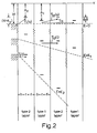
- the minimum read field is E 1 . It is the field required to equalise the energy levels on adjacent film layers so that tunnelling occurs between the layers without thermal activation. This is the minimum field which must be applied by voltage source 6.
- the field E 2 is the minimum write field. This is the field required to equalise the energy levels of an electron in the electrode 7 and an electron on the first film layer. Then tunnelling injection of electrons can occur without thermal activation. It is easy to arrange that E 2 is greater than E 1 (see below).
- Figure 3a shows the timing of the write field across the multilayer structure to give controlled injection of charge.
- the pulse train shown is that required to write 10101 into the memory.
- the raising of the field to E 2 does not affect the motion of the electrons already in the layers, for at the field E 1 they are already travelling across the device at their maximum rate.
- the film is formed of alternate layers of different materials labelled in Figure 2 as type 1 and type 2.
- the values of&A, A 2 W, b+d can readily be chosen to be such that E 2 >E 1 , which is a requirement for the device to operate. For most materials which one might use r i (e) ⁇ r 12 (e). So that the time needed to inject one bit into one layer is less than the time for the bits to be transferred fromone layer to another. If this is not the case, however, one can still operate the device by using a longer injection time and associating each bit with two or more layers.
- E 1 and E 2 are the minimum read and write fields and in practice both would normally be higher than the minimum values, with the read field being greater than E 1 but less than E 2 .
Landscapes
- Semiconductor Memories (AREA)
- Optical Record Carriers And Manufacture Thereof (AREA)
- Shift Register Type Memory (AREA)
Applications Claiming Priority (2)
| Application Number | Priority Date | Filing Date | Title |
|---|---|---|---|
| GB848409022A GB8409022D0 (en) | 1984-04-06 | 1984-04-06 | Information holding device |
| GB8409022 | 1984-04-06 |
Publications (2)
| Publication Number | Publication Date |
|---|---|
| EP0160426A2 true EP0160426A2 (de) | 1985-11-06 |
| EP0160426A3 EP0160426A3 (de) | 1988-01-07 |
Family
ID=10559330
Family Applications (1)
| Application Number | Title | Priority Date | Filing Date |
|---|---|---|---|
| EP85302439A Withdrawn EP0160426A3 (de) | 1984-04-06 | 1985-04-04 | Datenhalteschaltung |
Country Status (4)
| Country | Link |
|---|---|
| US (1) | US4670860A (de) |
| EP (1) | EP0160426A3 (de) |
| JP (1) | JPS60243900A (de) |
| GB (1) | GB8409022D0 (de) |
Cited By (2)
| Publication number | Priority date | Publication date | Assignee | Title |
|---|---|---|---|---|
| GB2185352A (en) * | 1986-01-14 | 1987-07-15 | Olympus Optical Co | Three-dimensional tunnel memory device |
| EP0437278A1 (de) * | 1990-01-12 | 1991-07-17 | Matsushita Electric Industrial Co., Ltd. | Verfahren zur Herstellung eines Überzuges aus organischen monomolekularen Schichten und chemisches Absorptionsmittel für dieses Verfahren |
Families Citing this family (17)
| Publication number | Priority date | Publication date | Assignee | Title |
|---|---|---|---|---|
| FI77679C (fi) * | 1987-02-23 | 1989-04-10 | K & V Licencing Oy | Filmaggregat och foerfarande foer dess framstaellning. |
| JP2680849B2 (ja) * | 1988-08-29 | 1997-11-19 | オリンパス光学工業株式会社 | 三次元メモリ素子およびその制御方法 |
| US4877952A (en) * | 1988-10-11 | 1989-10-31 | American Telephone And Telegraph Company | Faser cavity optical memory with optical storage and readout |
| DE69032949T2 (de) * | 1989-03-07 | 1999-08-12 | Matsushita Electric Industrial Co., Ltd., Kadoma, Osaka | Plattenwechsler |
| US5327373A (en) * | 1992-08-21 | 1994-07-05 | Board Of Regents, The University Of Texas System | Optoelectronic memories with photoconductive thin films |
| US5761115A (en) * | 1996-05-30 | 1998-06-02 | Axon Technologies Corporation | Programmable metallization cell structure and method of making same |
| US6381169B1 (en) | 1999-07-01 | 2002-04-30 | The Regents Of The University Of California | High density non-volatile memory device |
| US6208553B1 (en) | 1999-07-01 | 2001-03-27 | The Regents Of The University Of California | High density non-volatile memory device incorporating thiol-derivatized porphyrins |
| US6324091B1 (en) | 2000-01-14 | 2001-11-27 | The Regents Of The University Of California | Tightly coupled porphyrin macrocycles for molecular memory storage |
| CA2377671C (en) * | 1999-07-01 | 2011-01-04 | David F. Bocian | High density non-volatile memory device |
| US6212093B1 (en) | 2000-01-14 | 2001-04-03 | North Carolina State University | High-density non-volatile memory devices incorporating sandwich coordination compounds |
| EP1249021A4 (de) * | 2000-01-14 | 2007-03-28 | Univ North Carolina State | Substrate mit vernetzten sndwichkoordinationsverbindungspolymeren und verfahren für deren anwendung |
| US6272038B1 (en) | 2000-01-14 | 2001-08-07 | North Carolina State University | High-density non-volatile memory devices incorporating thiol-derivatized porphyrin trimers |
| WO2002077633A1 (en) * | 2001-03-23 | 2002-10-03 | The Regents Of The University Of California | Open circuit potential amperometry and voltammetry |
| US6728129B2 (en) * | 2002-02-19 | 2004-04-27 | The Regents Of The University Of California | Multistate triple-decker dyads in three distinct architectures for information storage applications |
| US7010644B2 (en) * | 2002-08-29 | 2006-03-07 | Micron Technology, Inc. | Software refreshed memory device and method |
| US20060238696A1 (en) * | 2005-04-20 | 2006-10-26 | Chien-Hui Wen | Method of aligning negative dielectric anisotropic liquid crystals |
Family Cites Families (5)
| Publication number | Priority date | Publication date | Assignee | Title |
|---|---|---|---|---|
| US2833936A (en) * | 1956-01-04 | 1958-05-06 | Ibm | Electrooptical shift register system |
| US3836989A (en) * | 1973-02-15 | 1974-09-17 | Agency Ind Science Techn | Bulk semiconductor device |
| NL7309000A (de) * | 1973-06-28 | 1974-12-31 | ||
| US4431263A (en) * | 1979-06-25 | 1984-02-14 | University Patents, Inc. | Novel nonlinear optical materials and processes employing diacetylenes |
| US4534015A (en) * | 1981-10-05 | 1985-08-06 | Qmc Industrial Research Limited | Information holding device |
-
1984
- 1984-04-06 GB GB848409022A patent/GB8409022D0/en active Pending
-
1985
- 1985-04-04 EP EP85302439A patent/EP0160426A3/de not_active Withdrawn
- 1985-04-04 US US06/719,876 patent/US4670860A/en not_active Expired - Fee Related
- 1985-04-05 JP JP60071301A patent/JPS60243900A/ja active Pending
Cited By (4)
| Publication number | Priority date | Publication date | Assignee | Title |
|---|---|---|---|---|
| GB2185352A (en) * | 1986-01-14 | 1987-07-15 | Olympus Optical Co | Three-dimensional tunnel memory device |
| GB2185352B (en) * | 1986-01-14 | 1989-11-29 | Olympus Optical Co | Three-dimensional tunnel memory device |
| EP0437278A1 (de) * | 1990-01-12 | 1991-07-17 | Matsushita Electric Industrial Co., Ltd. | Verfahren zur Herstellung eines Überzuges aus organischen monomolekularen Schichten und chemisches Absorptionsmittel für dieses Verfahren |
| US5246740A (en) * | 1990-01-12 | 1993-09-21 | Matsushita Electric Industrial Co., Ltd. | Process for preparing a lamination of organic monomolecular films, and a chemical adsorbent used for the process |
Also Published As
| Publication number | Publication date |
|---|---|
| EP0160426A3 (de) | 1988-01-07 |
| JPS60243900A (ja) | 1985-12-03 |
| US4670860A (en) | 1987-06-02 |
| GB8409022D0 (en) | 1984-05-16 |
Similar Documents
| Publication | Publication Date | Title |
|---|---|---|
| EP0160426A2 (de) | Datenhalteschaltung | |
| US3720922A (en) | Charge coupled memory | |
| US3930255A (en) | Analog to digital conversion by charge transfer device | |
| US4864168A (en) | Process for controlling an optical pnpn thyristor to be driven | |
| GB2129595A (en) | Improvements in or relating to display devices | |
| EP1103980A3 (de) | Nichtflüchtiger Halbleiterspeicher mit Zwei-Bitzellen | |
| GB1414228A (en) | Semiconductor storage devices | |
| DE2557359A1 (de) | Gegen datenverlust bei netzausfall gesicherter dynamischer speicher | |
| GB1351421A (en) | Electron beam addressable semiconductor memory | |
| US4007446A (en) | Multiphase series-parallel-series charge-coupled device registers | |
| US4024514A (en) | Multiphase series-parallel-series charge-coupled device registers with simplified input clocking | |
| JPH08510867A (ja) | メモリ材料及びその製造方法 | |
| EP0077135B1 (de) | Informationspeichervorrichtung mit einem mehrschichtigen Langmuir-Blodgett film | |
| EP0123435A3 (de) | Datenhalteanordnung | |
| US4813016A (en) | Tunnel memory device having a multi-layered Langmuir-Blodgett film | |
| US4117546A (en) | Interlaced ccd memory | |
| EP0550354B1 (de) | Verbesserte Bildquelle mit hoher Auflösung | |
| EP0739025A3 (de) | Adressierungsstruktur unter Verwendung einer Gasmischung mit niedriger Entionisierungszeit | |
| JPH06224411A (ja) | ロジック素子 | |
| US3829885A (en) | Charge coupled semiconductor memory device | |
| WO1996024137A3 (en) | Circuits, systems and methods for improving row select speed in a row select memory device | |
| US5574438A (en) | Method for transferring information, and in particular for performing a logic operation, using electron beams | |
| EP0389693B1 (de) | EPROM, der eine mehrfache Verwendung der Bitleitungskontakte ermöglicht | |
| US4453232A (en) | Device for generating magnetic bubbles with a high bit rate | |
| JP2000030467A (ja) | 記憶方法および記憶装置ならびに情報処理方法および情報処理装置 |
Legal Events
| Date | Code | Title | Description |
|---|---|---|---|
| PUAI | Public reference made under article 153(3) epc to a published international application that has entered the european phase |
Free format text: ORIGINAL CODE: 0009012 |
|
| AK | Designated contracting states |
Designated state(s): DE FR GB |
|
| PUAL | Search report despatched |
Free format text: ORIGINAL CODE: 0009013 |
|
| AK | Designated contracting states |
Kind code of ref document: A3 Designated state(s): DE FR GB |
|
| RHK1 | Main classification (correction) |
Ipc: G11C 21/00 |
|
| STAA | Information on the status of an ep patent application or granted ep patent |
Free format text: STATUS: THE APPLICATION IS DEEMED TO BE WITHDRAWN |
|
| 18D | Application deemed to be withdrawn |
Effective date: 19880708 |
|
| RIN1 | Information on inventor provided before grant (corrected) |
Inventor name: WILSON, EDWARD GUY |