EP0155039B1 - Current-source arrangement - Google Patents
Current-source arrangement Download PDFInfo
- Publication number
- EP0155039B1 EP0155039B1 EP85200254A EP85200254A EP0155039B1 EP 0155039 B1 EP0155039 B1 EP 0155039B1 EP 85200254 A EP85200254 A EP 85200254A EP 85200254 A EP85200254 A EP 85200254A EP 0155039 B1 EP0155039 B1 EP 0155039B1
- Authority
- EP
- European Patent Office
- Prior art keywords
- current
- transistor
- base
- resistor
- collector
- Prior art date
- Legal status (The legal status is an assumption and is not a legal conclusion. Google has not performed a legal analysis and makes no representation as to the accuracy of the status listed.)
- Expired
Links
- 238000012886 linear function Methods 0.000 description 4
- 230000001419 dependent effect Effects 0.000 description 3
Images
Classifications
-
- G—PHYSICS
- G05—CONTROLLING; REGULATING
- G05F—SYSTEMS FOR REGULATING ELECTRIC OR MAGNETIC VARIABLES
- G05F3/00—Non-retroactive systems for regulating electric variables by using an uncontrolled element, or an uncontrolled combination of elements, such element or such combination having self-regulating properties
- G05F3/02—Regulating voltage or current
- G05F3/08—Regulating voltage or current wherein the variable is DC
- G05F3/10—Regulating voltage or current wherein the variable is DC using uncontrolled devices with non-linear characteristics
- G05F3/16—Regulating voltage or current wherein the variable is DC using uncontrolled devices with non-linear characteristics being semiconductor devices
- G05F3/20—Regulating voltage or current wherein the variable is DC using uncontrolled devices with non-linear characteristics being semiconductor devices using diode- transistor combinations
- G05F3/26—Current mirrors
-
- G—PHYSICS
- G05—CONTROLLING; REGULATING
- G05F—SYSTEMS FOR REGULATING ELECTRIC OR MAGNETIC VARIABLES
- G05F3/00—Non-retroactive systems for regulating electric variables by using an uncontrolled element, or an uncontrolled combination of elements, such element or such combination having self-regulating properties
- G05F3/02—Regulating voltage or current
- G05F3/08—Regulating voltage or current wherein the variable is DC
- G05F3/10—Regulating voltage or current wherein the variable is DC using uncontrolled devices with non-linear characteristics
- G05F3/16—Regulating voltage or current wherein the variable is DC using uncontrolled devices with non-linear characteristics being semiconductor devices
- G05F3/20—Regulating voltage or current wherein the variable is DC using uncontrolled devices with non-linear characteristics being semiconductor devices using diode- transistor combinations
- G05F3/22—Regulating voltage or current wherein the variable is DC using uncontrolled devices with non-linear characteristics being semiconductor devices using diode- transistor combinations wherein the transistors are of the bipolar type only
- G05F3/222—Regulating voltage or current wherein the variable is DC using uncontrolled devices with non-linear characteristics being semiconductor devices using diode- transistor combinations wherein the transistors are of the bipolar type only with compensation for device parameters, e.g. Early effect, gain, manufacturing process, or external variations, e.g. temperature, loading, supply voltage
- G05F3/227—Regulating voltage or current wherein the variable is DC using uncontrolled devices with non-linear characteristics being semiconductor devices using diode- transistor combinations wherein the transistors are of the bipolar type only with compensation for device parameters, e.g. Early effect, gain, manufacturing process, or external variations, e.g. temperature, loading, supply voltage producing a current or voltage as a predetermined function of the supply voltage
Definitions
- the invention relates to a current-source arrangement comprising a. first current-mirror circuit having a first current multiplication factor and comprising a first transistor which has a collector coupled to an input of the first current-mirror circuit and which has a low impedance connection between the collector and the base, and comprising a second transistor having a base-emitted junction arranged in parallel with the base-emitter junction of the first transistor and comprising a first resistor arranged in parallel with the base-emitter junction of the first transistor.
- a current-source arrangement of the type specified in the opening paragraph is characterized in that the current-source arrangement further comprises between a first and second power supply terminal a series arrangement of a second resistor and the base-emitter junction of a third transistor whose collector is coupled to the input of the first current-mirror circuit and a second current-mirror circuit having a second current multiplication factor and an input which is coupled to the collector of the second transistor and an output which is coupled to the base of the third transistor and that the resistance value of the first resistor is substantially equal to the quotient of the resistance value of the second resistor and the product of the base-emitter voltage of the third transistor and the current multiplication factors of the first and second current mirror circuits.
- This current-source arrangement contains just one base-emitter junction voltage in series with a reference current determining resistor. So the minimum operating supply voltage is substantially one base-emitter junction voltage.
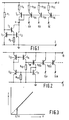
- Figure 1 shows a known current source arrangement.
- the emitter area of transistor T 2 is equal to that of transistor T 1 .
- the collector of transistor T 3 is connected to the collector of transistor T 2 .
- the collector of transistor T 2 is connected to the input 4 of a multiple current mirror which is shown in simplified form.
- the current mirror comprises a PNP-transistor T 4 connected as a diode, a resistor R 4 being included in its emitter . circuit.
- the base of transistor T 4 is connected to the bases of a plurality of transistors T SA , T SB and i T sc , resistors R 5A , R 58 and R sc being arranged in the respective emitter circuits.
- the supply-voltage dependent current can be taken from the collector terminals 5A, 5B and 5C.
- the resistors R 4 , R SA , R 5B and R sc are not essential and merely serve to improve the equality of the output currents.
- the circuit arrangement operates as follows. If the supply voltage is V s the current flowing in the resistor R 1 is equal to (V S -2V BE )/R.
- the current mirror comprising the transistors T 1 , T 2 and T 3 , of which transistors T 1 and T 2 have equal emitter areas, this current is reproduced in the collector circuit of transistor T 2 .
- the base-emitter voltage of transistor T 1 appears across the resistor R 2 , so that a current 2V BE/R flows through this resistor. This current is supplied by transistor T 3 .
- the current which flows in the collector circuit of transistor T 3 is also 2V BE /R.
- This current is added to the collector current of transistor T 2 , so that the common collector current of transistors T 2 and T 3 is equal to V s /R.
- This current which increases as a linear function of the supply voltage, is applied to the input 4 of the current-mirror circuit, so that currents which increase as linear functions of the supply voltage are available on outputs 5A, 5B and 5C, the absolute values of the currents being dependent on the ratio between the respective resistor R SA , R 5B and R 5c and the resistor R 4 .
- the collector of transistor T 10 is connected to the input of a first current-mirror circuit comprising a transistor T 11 connected as a diode and a transistor T 12 whose base-emitter junction is arranged in parallel with that of transistor T 11 .
- the emitter area of transistor T 11 is equal to that of transistor T 12 .
- the collector of transistor T 12 is connected to the input of a second current-mirror circuit comprising a transistor T 13 connected as a diode and a transistor T 14 whose base-emitter junction is connected in parallel with that of transistor T 13 and whose collector is connected to the base of transistor T 10 .
- Transistors T 13 and T 14 have equal emitter areas. A current which increases as a linear function of the supply voltage is available on the collector terminals 15A and 15B of transistors T 15A and T 15B , whose bases are connected to that of transistor T 10 . The arrangement then operates as follows.
- transistor T 10 Since transistor T 10 must also supply the current which is to be supplied to the resistor R 10 via the current mirrors T 11 , T 12 and T 13 , T 14 , a total current equal to V s /R will flow in the collector of transistor T 10 when the base currents of transistors T 11 and T 12 are ignored. This total current increases directly proportionally to the supply voltage.
- Figure 3 shows the current-voltage characteristic of the arrangement.
- the voltage-dependent current V s /R can be taken from the collector terminals 15A and 15B of the transistors T 15A and T 15B .
- transistors T 11 and T 12 have equal emitter areas, so that the collector current of transistor T 10 is equal to the current through resistor R 10 .
- transistors T 11 and T 12 may have different emitter areas.
- the collector current of transistor T 10 is then equal to the product of the overall gain factor of the current mirrors T 11 , T 12 and T 13 , T 14 and the current through resistor R 1o .
- the resistance value of resistor R 11 must then be reduced by this factor.
- NPN transistors may be replaced by PNP transistors and the other way round.
- resistors of equal value may be arranged in the emitter circuits of transistors T 11 and T 12 and any other known current mirror arrangement may be used for the current mirror circuit T 13 , T 14 .
Landscapes
- Engineering & Computer Science (AREA)
- Physics & Mathematics (AREA)
- Microelectronics & Electronic Packaging (AREA)
- Nonlinear Science (AREA)
- Electromagnetism (AREA)
- General Physics & Mathematics (AREA)
- Radar, Positioning & Navigation (AREA)
- Automation & Control Theory (AREA)
- Control Of Electrical Variables (AREA)
- Amplifiers (AREA)
Description
- The invention relates to a current-source arrangement comprising a. first current-mirror circuit having a first current multiplication factor and comprising a first transistor which has a collector coupled to an input of the first current-mirror circuit and which has a low impedance connection between the collector and the base, and comprising a second transistor having a base-emitted junction arranged in parallel with the base-emitter junction of the first transistor and comprising a first resistor arranged in parallel with the base-emitter junction of the first transistor.
- Such a current-source arrangement may be used for general purposes in integrated circuits and in particular integrated amplifier circuits.
- Such a current-source arrangement is known from Figure 2 of US-A-4,443,753 (corresponding e.g. to EP-A-0 088 767, published on 21.09.1983). In this circuit the collector of the first transistor is coupled at the one hand to its base via the base-emitter junction of a further transistor and at the other hand to the positive supply terminal via a further resistor. The reference current flowing into the input of the first current-mirror circuit and which is reproduced at its output is determined by the quotient of the difference of the supply voltage and the base-emitter voltages of the first and further transistors and the resistance of the further resistor. To compensate the non-linear component in the output current of the first current-mirror circuit caused by the dependency of the base-emitter voltage of the first and further transistors the collector current of the further transistor is added to the output current of the first current-mirror circuit. This collector current is determined by the first resistor and by properly selecting its resistance value this current fully compensates the non-linear component in the output current of the first current-mirror circuit.
- Such a current-source is suitable for battery- powered amplifier circuits which require current-source arrangements which operate at very low supply voltages. Generally, it is also required that these amplifier circuits can operate at higher supply voltages of, for example, 6 to 9 V. In view of the higher powers to be delivered at higher supply voltages the current-source arrangements must then be capable of supplying larger output currents. However, the known current-source arrangement cannot operate at supply voltages lower than two base-emitter junction voltages.
- Therefore, it is the object of the invention to provide a current-source arrangement which is suitable for very low supply voltages and which supplies an output current which increases as a linear function of the supply voltage. According to the invention a current-source arrangement of the type specified in the opening paragraph is characterized in that the current-source arrangement further comprises between a first and second power supply terminal a series arrangement of a second resistor and the base-emitter junction of a third transistor whose collector is coupled to the input of the first current-mirror circuit and a second current-mirror circuit having a second current multiplication factor and an input which is coupled to the collector of the second transistor and an output which is coupled to the base of the third transistor and that the resistance value of the first resistor is substantially equal to the quotient of the resistance value of the second resistor and the product of the base-emitter voltage of the third transistor and the current multiplication factors of the first and second current mirror circuits.
- This current-source arrangement contains just one base-emitter junction voltage in series with a reference current determining resistor. So the minimum operating supply voltage is substantially one base-emitter junction voltage. The invention will now be described in more detail, by way of example, with reference to the drawing, in which
- Figure 1 shows a known current-source arrangement,
- Figure 2 shows a current source arrangement according to the invention, and
- Figure 3 shows a current-voltage characteristic of the arrangement shown in Figure 2.
- Figure 1 shows a known current source arrangement. The arrangement comprises the series arrangement of a resistor R1=R, the base-emitter junction of a transistor T3, and the base-emitter junction of a transistor T1 between the positive power-supply terminal 2 and the negative power-
supply terminal 3, in the present case earth, the base and the emitter of transistor T3 being connected to the collector and the base, respectively, of transistor T1. A resistor R2=R/2 and the base-emitter junction of a transistor T2 are arranged in parallel with the base-emitter junction of transistor T1. In the present example the emitter area of transistor T2 is equal to that of transistor T1. The collector of transistor T3 is connected to the collector of transistor T2. Further, the collector of transistor T2 is connected to the input 4 of a multiple current mirror which is shown in simplified form. The current mirror comprises a PNP-transistor T4 connected as a diode, a resistor R4 being included in its emitter . circuit. The base of transistor T4 is connected to the bases of a plurality of transistors TSA, TSB and i Tsc, resistors R5A, R58 and Rsc being arranged in the respective emitter circuits. The supply-voltage dependent current can be taken from thecollector terminals outputs - A current-source arrangement according to the invention will be described with reference to Figure 2. Between the positive power-
supply terminal 10 and the negative power-supply terminal 11, in the present case earth, the current-source arrangement comprises the series arrangement of the base-emitter junction of a transistor T10 and a resistor R10=R. The collector of transistor T10 is connected to the input of a first current-mirror circuit comprising a transistor T11 connected as a diode and a transistor T12 whose base-emitter junction is arranged in parallel with that of transistor T11. In the present example the emitter area of transistor T11 is equal to that of transistor T12. A resistor R11=R is connected between the base and the emitter of transistor T11. The collector of transistor T12 is connected to the input of a second current-mirror circuit comprising a transistor T13 connected as a diode and a transistor T14 whose base-emitter junction is connected in parallel with that of transistor T13 and whose collector is connected to the base of transistor T10. Transistors T13 and T14 have equal emitter areas. A current which increases as a linear function of the supply voltage is available on thecollector terminals collector terminals - . The invention is not limited to the aforementioned embodiment. Within the scope of the present invention other current-source arrangements based on the same principal can be designed by those skilled in the art.
Claims (1)
- A current-source arrangement comprising a first current-mirror circuit (T11, T12), having a first current multiplication factor and comprising a first transistor (T11), which has a collector coupled to an input of the first current-mirror circuit and which has a low impedance connection between the collector and the base, and comprising a second transistor (T12) having a base-emitter junction arranged in parallel with the base-emitter junction of the first transistor (T11) and comprising a first resistor (R11) arranged in parallel with the base-emitter junction of the first transistor (T11), characterized in that the current-source arrangement further comprises between a first (10) and second (11) power supply terminal a series arrangement of a second resistor (R10) and the base-emitter junction of a third transistor (T10) whose collector is coupled to the input of the first current-mirror circuit (T11, T12) and a second current-mirror circuit (T13, T14), having a second current multiplication factor and an input which is coupled to the collector of the second transistor (T12) and an output which is coupled to the base of the third transistor (Tlo), and that the resistance value of the first resistor (R11) is substantially equal to the quotient of the resistance value of the second resistor (Rio) and the product of the base-emitter voltage of the third transistor (Tio) and the current multiplication factors of the first and second current mirror circuits.
Applications Claiming Priority (2)
| Application Number | Priority Date | Filing Date | Title |
|---|---|---|---|
| NL8400636A NL8400636A (en) | 1984-02-29 | 1984-02-29 | POWER SOURCE SWITCH. |
| NL8400636 | 1984-02-29 |
Publications (2)
| Publication Number | Publication Date |
|---|---|
| EP0155039A1 EP0155039A1 (en) | 1985-09-18 |
| EP0155039B1 true EP0155039B1 (en) | 1989-10-18 |
Family
ID=19843565
Family Applications (1)
| Application Number | Title | Priority Date | Filing Date |
|---|---|---|---|
| EP85200254A Expired EP0155039B1 (en) | 1984-02-29 | 1985-02-25 | Current-source arrangement |
Country Status (9)
| Country | Link |
|---|---|
| US (1) | US4605892A (en) |
| EP (1) | EP0155039B1 (en) |
| JP (1) | JPH0682308B2 (en) |
| KR (1) | KR920009548B1 (en) |
| CA (1) | CA1210091A (en) |
| DE (1) | DE3573848D1 (en) |
| HK (1) | HK86691A (en) |
| NL (1) | NL8400636A (en) |
| SG (1) | SG85890G (en) |
Families Citing this family (10)
| Publication number | Priority date | Publication date | Assignee | Title |
|---|---|---|---|---|
| GB2186140B (en) * | 1986-01-30 | 1989-11-01 | Plessey Co Plc | Current source circuit |
| US4743833A (en) * | 1987-04-03 | 1988-05-10 | Cross Technology, Inc. | Voltage regulator |
| US4882533A (en) * | 1987-08-28 | 1989-11-21 | Unitrode Corporation | Linear integrated circuit voltage drop generator having a base-10-emitter voltage independent current source therein |
| GB2217937A (en) * | 1988-04-29 | 1989-11-01 | Philips Electronic Associated | Current divider circuit |
| US4864216A (en) * | 1989-01-19 | 1989-09-05 | Hewlett-Packard Company | Light emitting diode array current power supply |
| JPH03113613A (en) * | 1989-09-28 | 1991-05-15 | Sumitomo Electric Ind Ltd | Wide dynamic range current source circuit |
| US4958122A (en) * | 1989-12-18 | 1990-09-18 | Motorola, Inc. | Current source regulator |
| JP2001092545A (en) * | 1999-09-24 | 2001-04-06 | Mitsubishi Electric Corp | Self bias circuit |
| FR2821443B1 (en) * | 2001-02-26 | 2003-06-20 | St Microelectronics Sa | CURRENT SOURCE CAPABLE OF OPERATING AT LOW SUPPLY VOLTAGE AND AT CURRENT VARIATION WITH NEAR ZERO SUPPLY VOLTAGE |
| US6741119B1 (en) * | 2002-08-29 | 2004-05-25 | National Semiconductor Corporation | Biasing circuitry for generating bias current insensitive to process, temperature and supply voltage variations |
Citations (1)
| Publication number | Priority date | Publication date | Assignee | Title |
|---|---|---|---|---|
| EP0088767A1 (en) * | 1981-08-24 | 1983-09-21 | Advanced Micro Devices Inc | A second order temperature compensated band gap voltage reference. |
Family Cites Families (5)
| Publication number | Priority date | Publication date | Assignee | Title |
|---|---|---|---|---|
| US3886435A (en) * | 1973-08-03 | 1975-05-27 | Rca Corp | V' be 'voltage voltage source temperature compensation network |
| JPS5922245B2 (en) * | 1975-12-05 | 1984-05-25 | 日本電気株式会社 | Teiden Atsubias Cairo |
| JPS5482647A (en) * | 1977-12-14 | 1979-07-02 | Sony Corp | Transistor circuit |
| US4172992A (en) * | 1978-07-03 | 1979-10-30 | National Semiconductor Corporation | Constant current control circuit |
| JPS5866129A (en) * | 1981-10-15 | 1983-04-20 | Toshiba Corp | Constant current source circuit |
-
1984
- 1984-02-29 NL NL8400636A patent/NL8400636A/en not_active Application Discontinuation
-
1985
- 1985-02-25 DE DE8585200254T patent/DE3573848D1/en not_active Expired
- 1985-02-25 EP EP85200254A patent/EP0155039B1/en not_active Expired
- 1985-02-25 CA CA000475078A patent/CA1210091A/en not_active Expired
- 1985-02-26 US US06/705,763 patent/US4605892A/en not_active Expired - Fee Related
- 1985-02-26 JP JP60035415A patent/JPH0682308B2/en not_active Expired - Lifetime
- 1985-02-27 KR KR1019850001245A patent/KR920009548B1/en not_active Expired
-
1990
- 1990-10-24 SG SG858/90A patent/SG85890G/en unknown
-
1991
- 1991-10-31 HK HK866/91A patent/HK86691A/en unknown
Patent Citations (2)
| Publication number | Priority date | Publication date | Assignee | Title |
|---|---|---|---|---|
| EP0088767A1 (en) * | 1981-08-24 | 1983-09-21 | Advanced Micro Devices Inc | A second order temperature compensated band gap voltage reference. |
| US4443753A (en) * | 1981-08-24 | 1984-04-17 | Advanced Micro Devices, Inc. | Second order temperature compensated band cap voltage reference |
Also Published As
| Publication number | Publication date |
|---|---|
| EP0155039A1 (en) | 1985-09-18 |
| NL8400636A (en) | 1985-09-16 |
| HK86691A (en) | 1991-11-08 |
| JPS60204019A (en) | 1985-10-15 |
| KR850006737A (en) | 1985-10-16 |
| CA1210091A (en) | 1986-08-19 |
| US4605892A (en) | 1986-08-12 |
| SG85890G (en) | 1991-01-04 |
| KR920009548B1 (en) | 1992-10-19 |
| DE3573848D1 (en) | 1989-11-23 |
| JPH0682308B2 (en) | 1994-10-19 |
Similar Documents
| Publication | Publication Date | Title |
|---|---|---|
| US4951003A (en) | Differential transconductance circuit | |
| GB2143692A (en) | Low voltage ic current supply | |
| US4567426A (en) | Current stabilizer with starting circuit | |
| EP0139425B1 (en) | A constant current source circuit | |
| EP0155720B1 (en) | Cascode current source arrangement | |
| EP0155039B1 (en) | Current-source arrangement | |
| EP0039178B1 (en) | Integrated circuit for generating a reference voltage | |
| JP2542623B2 (en) | Current mirror circuit | |
| US4590419A (en) | Circuit for generating a temperature-stabilized reference voltage | |
| US5343141A (en) | Transistor overcurrent protection circuit | |
| EP0391055A2 (en) | Output stage for an operational amplifier | |
| US4501933A (en) | Transistor bridge voltage rectifier circuit | |
| EP0155717B1 (en) | Push-pull amplifier | |
| EP0132863A1 (en) | Protection circuit | |
| US4329598A (en) | Bias generator | |
| EP0397265B1 (en) | Bipolar transistor arrangement with distortion compensation | |
| JPH11505053A (en) | Reference voltage source with temperature compensation | |
| EP0133506A2 (en) | Output stage for power amplifiers | |
| CA1208313A (en) | Differential amplifier | |
| EP0110720B1 (en) | Current mirror circuit | |
| US4409558A (en) | Gain compensated transistor amplifier | |
| JPS5857814A (en) | Electronic impedance device | |
| JP2897515B2 (en) | Voltage-current converter | |
| EP0290277B1 (en) | A low noise integrated active load circuit | |
| US4829231A (en) | Current mirror having a high output voltage |
Legal Events
| Date | Code | Title | Description |
|---|---|---|---|
| PUAI | Public reference made under article 153(3) epc to a published international application that has entered the european phase |
Free format text: ORIGINAL CODE: 0009012 |
|
| AK | Designated contracting states |
Designated state(s): CH DE FR GB IT LI |
|
| 17P | Request for examination filed |
Effective date: 19860317 |
|
| 17Q | First examination report despatched |
Effective date: 19880121 |
|
| GRAA | (expected) grant |
Free format text: ORIGINAL CODE: 0009210 |
|
| AK | Designated contracting states |
Kind code of ref document: B1 Designated state(s): CH DE FR GB IT LI |
|
| REF | Corresponds to: |
Ref document number: 3573848 Country of ref document: DE Date of ref document: 19891123 |
|
| ITF | It: translation for a ep patent filed | ||
| ET | Fr: translation filed | ||
| PLBE | No opposition filed within time limit |
Free format text: ORIGINAL CODE: 0009261 |
|
| STAA | Information on the status of an ep patent application or granted ep patent |
Free format text: STATUS: NO OPPOSITION FILED WITHIN TIME LIMIT |
|
| 26N | No opposition filed | ||
| ITTA | It: last paid annual fee | ||
| PGFP | Annual fee paid to national office [announced via postgrant information from national office to epo] |
Ref country code: GB Payment date: 19950201 Year of fee payment: 11 |
|
| PGFP | Annual fee paid to national office [announced via postgrant information from national office to epo] |
Ref country code: FR Payment date: 19950222 Year of fee payment: 11 |
|
| ITPR | It: changes in ownership of a european patent |
Owner name: CAMBIO RAGIONE SOCIALE;PHILIPS ELECTRONICS N.V. |
|
| PGFP | Annual fee paid to national office [announced via postgrant information from national office to epo] |
Ref country code: DE Payment date: 19950424 Year of fee payment: 11 |
|
| REG | Reference to a national code |
Ref country code: CH Ref legal event code: PFA Free format text: PHILIPS ELECTRONICS N.V. |
|
| PGFP | Annual fee paid to national office [announced via postgrant information from national office to epo] |
Ref country code: CH Payment date: 19950526 Year of fee payment: 11 |
|
| REG | Reference to a national code |
Ref country code: FR Ref legal event code: CD |
|
| PG25 | Lapsed in a contracting state [announced via postgrant information from national office to epo] |
Ref country code: GB Effective date: 19960225 |
|
| PG25 | Lapsed in a contracting state [announced via postgrant information from national office to epo] |
Ref country code: LI Free format text: LAPSE BECAUSE OF NON-PAYMENT OF DUE FEES Effective date: 19960228 Ref country code: CH Free format text: LAPSE BECAUSE OF NON-PAYMENT OF DUE FEES Effective date: 19960228 |
|
| REG | Reference to a national code |
Ref country code: CH Ref legal event code: PL |
|
| GBPC | Gb: european patent ceased through non-payment of renewal fee |
Effective date: 19960225 |
|
| PG25 | Lapsed in a contracting state [announced via postgrant information from national office to epo] |
Ref country code: FR Effective date: 19961031 |
|
| PG25 | Lapsed in a contracting state [announced via postgrant information from national office to epo] |
Ref country code: DE Effective date: 19961101 |
|
| REG | Reference to a national code |
Ref country code: FR Ref legal event code: ST |