EP0154798A1 - Speicherchip zur Handhabung von Speicherbauelementen - Google Patents
Speicherchip zur Handhabung von Speicherbauelementen Download PDFInfo
- Publication number
- EP0154798A1 EP0154798A1 EP85101075A EP85101075A EP0154798A1 EP 0154798 A1 EP0154798 A1 EP 0154798A1 EP 85101075 A EP85101075 A EP 85101075A EP 85101075 A EP85101075 A EP 85101075A EP 0154798 A1 EP0154798 A1 EP 0154798A1
- Authority
- EP
- European Patent Office
- Prior art keywords
- memory
- address
- components
- chip
- signal
- Prior art date
- Legal status (The legal status is an assumption and is not a legal conclusion. Google has not performed a legal analysis and makes no representation as to the accuracy of the status listed.)
- Withdrawn
Links
Images

Classifications
-
- G—PHYSICS
- G06—COMPUTING OR CALCULATING; COUNTING
- G06F—ELECTRIC DIGITAL DATA PROCESSING
- G06F12/00—Accessing, addressing or allocating within memory systems or architectures
- G06F12/02—Addressing or allocation; Relocation
- G06F12/06—Addressing a physical block of locations, e.g. base addressing, module addressing, memory dedication
- G06F12/0615—Address space extension
- G06F12/0623—Address space extension for memory modules
-
- G—PHYSICS
- G11—INFORMATION STORAGE
- G11C—STATIC STORES
- G11C8/00—Arrangements for selecting an address in a digital store
- G11C8/18—Address timing or clocking circuits; Address control signal generation or management, e.g. for row address strobe [RAS] or column address strobe [CAS] signals
Definitions
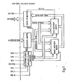
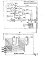
- Shown in greater detail in fig. 2 is the interrelation between the INTERNAL LOGIC/MEMORY TIMING BUFFER block and the ADDRESS BUFFER block.
Landscapes
- Engineering & Computer Science (AREA)
- Theoretical Computer Science (AREA)
- Physics & Mathematics (AREA)
- General Engineering & Computer Science (AREA)
- General Physics & Mathematics (AREA)
- Microelectronics & Electronic Packaging (AREA)
- Dram (AREA)
Applications Claiming Priority (2)
| Application Number | Priority Date | Filing Date | Title |
|---|---|---|---|
| IT83331/84A IT1181168B (it) | 1984-03-02 | 1984-03-02 | Procedimento di gestione componenti di memoria e piastra di memoria utilizzante tale procedimento |
| IT8333184 | 1984-03-02 |
Publications (1)
| Publication Number | Publication Date |
|---|---|
| EP0154798A1 true EP0154798A1 (de) | 1985-09-18 |
Family
ID=11320254
Family Applications (1)
| Application Number | Title | Priority Date | Filing Date |
|---|---|---|---|
| EP85101075A Withdrawn EP0154798A1 (de) | 1984-03-02 | 1985-02-01 | Speicherchip zur Handhabung von Speicherbauelementen |
Country Status (2)
| Country | Link |
|---|---|
| EP (1) | EP0154798A1 (de) |
| IT (1) | IT1181168B (de) |
Citations (3)
| Publication number | Priority date | Publication date | Assignee | Title |
|---|---|---|---|---|
| US4200919A (en) * | 1978-12-05 | 1980-04-29 | The United States Of America As Represented By The Secretary Of The Navy | Apparatus for expanding the memory of a mini-computer system |
| GB2091008A (en) * | 1981-01-14 | 1982-07-21 | Hitachi Ltd | A semiconductor memory |
| EP0080902A2 (de) * | 1981-12-02 | 1983-06-08 | Fujitsu Limited | Halbleiterspeicheranlage |
-
1984
- 1984-03-02 IT IT83331/84A patent/IT1181168B/it active
-
1985
- 1985-02-01 EP EP85101075A patent/EP0154798A1/de not_active Withdrawn
Patent Citations (3)
| Publication number | Priority date | Publication date | Assignee | Title |
|---|---|---|---|---|
| US4200919A (en) * | 1978-12-05 | 1980-04-29 | The United States Of America As Represented By The Secretary Of The Navy | Apparatus for expanding the memory of a mini-computer system |
| GB2091008A (en) * | 1981-01-14 | 1982-07-21 | Hitachi Ltd | A semiconductor memory |
| EP0080902A2 (de) * | 1981-12-02 | 1983-06-08 | Fujitsu Limited | Halbleiterspeicheranlage |
Non-Patent Citations (2)
| Title |
|---|
| IBM TECHNICAL DISCLOSURE BULLETIN, vol. 15, no. 10, March 1973, pages 3050-3051, New York, US; B.E. PHELPS: "Addressing combined memories" * |
| PATENTS ABSTRACTS OF JAPAN, vol. 6, no. 171 (P-140) [1049], September 1982, & JP - A - 57 89 146 (TOKYO SHIBAURA DENKI K.K.) 03-06-1982 * |
Also Published As
| Publication number | Publication date |
|---|---|
| IT1181168B (it) | 1987-09-23 |
| IT8483331A0 (it) | 1984-03-02 |
Similar Documents
| Publication | Publication Date | Title |
|---|---|---|
| US4376300A (en) | Memory system employing mostly good memories | |
| US4586167A (en) | Semiconductor memory device | |
| US4058851A (en) | Conditional bypass of error correction for dual memory access time selection | |
| KR100273090B1 (ko) | 메모리시험장치 | |
| EP0096782B1 (de) | On-Line Neuausrichtung von Speicherfehlern | |
| JPH0877794A (ja) | 半導体記憶装置 | |
| US7136985B2 (en) | Method and system for fast data access using a memory array | |
| EP0025801A1 (de) | Zugriffssystem für speichermodule | |
| JPS635839B2 (de) | ||
| EP0143647A2 (de) | Halbleiterspeicheranordnung | |
| US4523313A (en) | Partial defective chip memory support system | |
| US5611042A (en) | Data error detection and correction for a shared SRAM | |
| US4473877A (en) | Parasitic memory expansion for computers | |
| US4805173A (en) | Error control method and apparatus | |
| US5546569A (en) | Apparatus for writing data to and reading data from a multi-port RAM in a single clock cycle | |
| JPS5953630B2 (ja) | メモリ−のアドレス指定装置 | |
| WO1984000630A1 (en) | Virtual memory addressing system and method | |
| EP0154798A1 (de) | Speicherchip zur Handhabung von Speicherbauelementen | |
| EP0215455B1 (de) | Schreibeschaltung für eine EPROM-Anordnung eines mikrorechners | |
| US5708613A (en) | High performance redundancy in an integrated memory system | |
| EP0153015A2 (de) | Integrierte Wafer-Scale-Schaltungen | |
| US4795984A (en) | Multi-marker, multi-destination timing signal generator | |
| KR0179166B1 (ko) | 디지탈 영상신호처리용 메모리장치 | |
| US6108762A (en) | Address processor and method therefor | |
| WO1992020068A1 (en) | Fast memory system employing mostly good memories |
Legal Events
| Date | Code | Title | Description |
|---|---|---|---|
| PUAI | Public reference made under article 153(3) epc to a published international application that has entered the european phase |
Free format text: ORIGINAL CODE: 0009012 |
|
| AK | Designated contracting states |
Designated state(s): AT BE CH DE FR GB IT LI LU NL SE |
|
| 17P | Request for examination filed |
Effective date: 19851111 |
|
| 17Q | First examination report despatched |
Effective date: 19870219 |
|
| STAA | Information on the status of an ep patent application or granted ep patent |
Free format text: STATUS: THE APPLICATION IS DEEMED TO BE WITHDRAWN |
|
| 18D | Application deemed to be withdrawn |
Effective date: 19870702 |
|
| RIN1 | Information on inventor provided before grant (corrected) |
Inventor name: NADALUTTI, GIANFRANCO |