EP0154796A2 - Manufacturing process for layered metallic multichannel plates for an image intensifier, and use of plates so manufactured - Google Patents
Manufacturing process for layered metallic multichannel plates for an image intensifier, and use of plates so manufactured Download PDFInfo
- Publication number
- EP0154796A2 EP0154796A2 EP85101037A EP85101037A EP0154796A2 EP 0154796 A2 EP0154796 A2 EP 0154796A2 EP 85101037 A EP85101037 A EP 85101037A EP 85101037 A EP85101037 A EP 85101037A EP 0154796 A2 EP0154796 A2 EP 0154796A2
- Authority
- EP
- European Patent Office
- Prior art keywords
- layers
- produced
- plates
- intermediate layers
- negative
- Prior art date
- Legal status (The legal status is an assumption and is not a legal conclusion. Google has not performed a legal analysis and makes no representation as to the accuracy of the status listed.)
- Granted
Links
Images

Classifications
-
- H—ELECTRICITY
- H01—ELECTRIC ELEMENTS
- H01J—ELECTRIC DISCHARGE TUBES OR DISCHARGE LAMPS
- H01J43/00—Secondary-emission tubes; Electron-multiplier tubes
- H01J43/04—Electron multipliers
- H01J43/06—Electrode arrangements
- H01J43/18—Electrode arrangements using essentially more than one dynode
- H01J43/24—Dynodes having potential gradient along their surfaces
- H01J43/246—Microchannel plates [MCP]
-
- H—ELECTRICITY
- H01—ELECTRIC ELEMENTS
- H01J—ELECTRIC DISCHARGE TUBES OR DISCHARGE LAMPS
- H01J9/00—Apparatus or processes specially adapted for the manufacture, installation, removal, maintenance of electric discharge tubes, discharge lamps, or parts thereof; Recovery of material from discharge tubes or lamps
- H01J9/02—Manufacture of electrodes or electrode systems
- H01J9/12—Manufacture of electrodes or electrode systems of photo-emissive cathodes; of secondary-emission electrodes
- H01J9/125—Manufacture of electrodes or electrode systems of photo-emissive cathodes; of secondary-emission electrodes of secondary emission electrodes
-
- H—ELECTRICITY
- H01—ELECTRIC ELEMENTS
- H01J—ELECTRIC DISCHARGE TUBES OR DISCHARGE LAMPS
- H01J2201/00—Electrodes common to discharge tubes
- H01J2201/32—Secondary emission electrodes
Definitions
- the invention relates to a method for producing layered multi-channel plates with metal dynodes for amplifying optical images or other areal signal distributions by means of secondary electron multiplication, and to the use of multi-channel plates produced in this way.
- the invention is based on the object of proposing a method for producing layered multi-channel image intensifier plates of the generic type in which the separate production of the dynodes and their subsequent stacking and mutual alignment are avoided.
- layered multi-channel plates with metal dynodes can be produced, with which a similarly high spatial resolution and a similarly high transparency as in the known image intensifier plates made of glass can be achieved without the limitations typical for glass image intensifier plates in the gain factor and in the signal repetition frequency must be accepted.
- the method of the invention can be modified in accordance with claim 2 to reduce the cost of mass production of multi-channel plates of the type described in claim 1.
- a metallic positive mold is produced with a primary negative mold of the layered multi-channel plate using a metal electrode connected to it by galvanic molding and subsequent removal of the primary negative mold, after which several secondary moldings are made by repeated molding of the metallic positive mold
- Negative forms of the layered multi-channel plate be produced that take on the role of the primary negative form in the further implementation of the method.
- Non-adhesive reactive resins are particularly suitable as impression materials. Further details relating to the impression can be found, for example, in DE-PS 32 06 820.
- the dynodes are mutually electrically isolated by removing the intermediate layers. If layered multi-channel plates with a larger diameter are to be produced in this way, it can be advantageous to mount electrically insulating supports not only on the channel-free edge, but also within the image field of the multi-channel plate, which is penetrated by channels.
- the supports in the area of the layered multi-channel plates, which are interspersed with channels only cover about 1 per mille of the image field, they can be perceived as a disadvantage if the transmission quality is particularly high.
- a modification of the method of the invention according to claim 4 is provided.
- Aluminum is particularly suitable for the subsequent conversion of the intermediate layer into an electrical insulator described there.
- the small wall thicknesses typical of multi-channel plates with high transparency it can be converted in a known manner with oxidizing agent working in the liquid and / or gaseous phase into the electrically excellent insulating Al 2 O 3 .
- the area penetrated by channels is to be surrounded by a channel-free area to facilitate assembly or the electrical connections, this area must consist of numerous thin walls to ensure the conversion of the more easily oxidizable material into an insulator.
- the limitation to thin walls does not apply if the intermediate layers, according to claim 5, are produced by complete or partial oxidation of electrodeposited aluminum layers.
- the oxidation of the aluminum layers can be carried out both chemically and electrochemically.
- an inclination of the channels against the plate surface favors the collision of the primary particles with the channel walls and thus the desired electron release.
- the inclination of the channels is achieved by mutual displacement of the dynodes during stacking.
- dislocations occur between the mutually assigned channels of the adjacent dynodes, which lead to a reduction in transparency and / or the spatial resolution.
- the inclination of the channels can be brought about by appropriate orientation of the plate surface with respect to the direction of propagation of the high-energy radiation without loss of transparency and / or spatial resolution.
- a channel curvature aimed at suppressing the acceleration of parasitic ions can likewise only be achieved in the previously known methods for producing layered multi-channel plates only by mutually displacing the dynodes with the disadvantages mentioned above.
- these disadvantages can be avoided in that, according to claim 7, before the formation of the dynodes and intermediate layers, the negative shapes of the channels are bent at a higher temperature by a uniformly acting force, for example a centrifugal force.
- the layered multi-channel plates can be assembled in such a way that the channel openings of layered multi-channel plates lying on top of one another are aligned with one another. This avoids losses in transparency and / or spatial resolution.
- Both corpuscular rays and electromagnetic waves can be considered as high-energy radiation. While the use of electromagnetic waves to produce the desired structures uses masks in a known manner, the structures can also be generated by electromagnetic control when using corpuscular beams.
- the X-ray radiation (“synchrotron radiation") generated by the electron synchrotons, which is characterized by high intensity with a small aperture angle.
- the choice of the material that can be changed by high-energy radiation depends on the type of high-energy radiation, and corresponding regulations can be found, for example, in DE-PS 29 22 642 and DE-OS 32 21 981.
- PMMA polymethyl methacrylate
- the secondary electron yield factor of those with channels can be known in a manner known per se provided metal layers may be increased considerably.
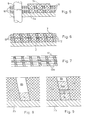
- the PMMA plate 1 is irradiated with synchrotron radiation 3 via an X-ray mask, which is directed obliquely to the surfaces of the PMMA plate 1 and the X-ray mask.
- the x-ray mask consists of a carrier 4 which only weakly absorbs the x-ray radiation and an absorber 5 which strongly absorbs the x-ray radiation, by means of which the cross-sectional shapes and the positions of the negative shapes of the channels are determined.
- the individual structures of the absorber 5 correspond to the cross-sectional shapes of the negative shapes of the channels. Due to the high-intensity parallel synchrotron radiation, the PMMA in the areas 6 not covered by the absorber will undergo chemical radiation changes. These areas 6 irradiated in this way are removed by introducing the PMMA plate into a developer solution, so that a multichannel negative shape with columnar PMMA structures 7 and lattice-shaped free spaces 8 according to FIG. 3 is produced.
- the columnar PMMA structures 7 have a hexagonal cross-sectional shape with a width of approximately 30 ⁇ m , the width of the free spaces 8 between the PMMA structures 7 is approximately 4 ⁇ m.
- FIG. 4 When producing a multi-channel plate with individual dynodes, which are firmly connected to electrically insulating supports, the negative form shown in FIG. 4 is assumed, which, in addition to the metal electrode 2a, the columnar PMMA structures 7a with lattice-free spaces 8a, as they are were already shown in Figure 3, additionally contains supports 9 made of electrically insulating material. In the free spaces 8a layers of nickel 10 and copper 11 are deposited galvanically alternately so that a formed-construction according to "Fig. 5.
- the PMMA structures 7a with an organic solvent and the copper layers 11 and the electrode 2a with an etch, which does not attack the nickel layers 10, are first removed, so that a sequence of mutually insulated dynode layers, which are fixed to the electrically insulating supports 9 connected, remains.
- the negative mold 7 shown in FIG. 3 is used in the production of layered multi-channel plates made of dynodes and intermediate layers subsequently produced. 6, layers of nickel 12 and aluminum 13 are alternately deposited in the free spaces 8 of the negative mold 7. After removal of the negative mold 7 with an organic solvent and the electrode 2 with an etch which does not attack either the nickel layers 12 or the aluminum layers 13, the aluminum layers become known
Landscapes
- Engineering & Computer Science (AREA)
- Manufacturing & Machinery (AREA)
- Electron Tubes For Measurement (AREA)
- Moulds For Moulding Plastics Or The Like (AREA)
- Pressure Welding/Diffusion-Bonding (AREA)
- Particle Accelerators (AREA)
- Electroplating Methods And Accessories (AREA)
- Laminated Bodies (AREA)
- Paper (AREA)
Abstract
Die Erfindung betrifft ein Verfahren zur Herstellung geschichteter Vielkanalplatten mit Dynoden aus Metall für die Verstärkung optischer Bilder oder anderer flächenhafter Signalverteilungen mittels Sekundärelektronenvervielfachung sowie deren Verwendung so hergestellter Vielkanalplatten. Die Aufgabe der Erfindung wird dadurch gelöst, daß
- a) zunächst eine Negativform der herzustellenden geschichteten Vielkanalplatten erzeugt wird, in dem in eine Platte durch partielles Bestrahlen und partielles Entfernen dieses Materials unter Ausnutzung der durch die Bestrahlung erzeugten unterschiedlichen Materialeigenschaften senkrecht oder schräg zur Plattenoberfläche die gitterförmigen Freiräume eingearbeitet werden, daß
- b) in die gitterförmigen Freiräume der Negativform unter Verwendung der mit ihr verbundenen Metallelektrode die Dynodenschichten galvanisch abwechselnd mit elektrisch leitenden oder isolierenden Zwischenschichten erzeugt werden, worauf
- c) die Negativform entfernt wird, und im Falle der Erzeugung elektrisch leitender Zwischenschichten diese entfernt oder in einen elektrischen Isolator umgewandelt werden.

- a) a negative form of the layered multi-channel plates to be produced is first produced, in which the lattice-shaped free spaces are worked into a plate by partially irradiating and partially removing this material, taking advantage of the different material properties generated by the irradiation, perpendicular or obliquely to the plate surface, in that
- b) in the lattice-shaped free spaces of the negative form, using the metal electrode connected to it, the dynode layers are produced alternately with electrically conductive or insulating intermediate layers, whereupon
- c) the negative form is removed, and in the case of the production of electrically conductive intermediate layers, these are removed or converted into an electrical insulator.
Description
Die Erfindung betrifft ein Verfahren zur Herstellung geschichteter Vielkanalplatten mit Dynoden aus Metall für die Verstärkung optischer Bilder oder anderer flächenhafter Signalverteilungen mittels Sekundärelektronenvervielfachung sowie die Verwendung so hergestellter Vielkanalplatten.The invention relates to a method for producing layered multi-channel plates with metal dynodes for amplifying optical images or other areal signal distributions by means of secondary electron multiplication, and to the use of multi-channel plates produced in this way.
Es ist bekannt, optische Bilder oder andere flächenhafte Signalverteilungen mit geschichteten Vielkanalplatten aus Metall zu verstärken (s. DE-OS 31- 50 257 und DE-PS 24 14 658). Sie bestehen aus zahlreichen elektrisch gegeneinander isolierten, mit eng benachbarten Löchern versehenen Metallschichten, die so gestapelt sind, daß die Löcher eng benachbarte, senkrecht zur Plattenoberfläche verlaufende Kanäle bilden. Die Schichten sind einzeln so an eine Spannungsquelle angeschlossen, daß sich zwischen ihnen ein stufenweiser Potentialanstieg ergibt. Die Kanäle erhalten dadurch die Funktion von Sekundärelektronenvervielfachern, wobei die mit Löchern versehenen Metallschichten die Dynoden bilden. Die Löcher der einzelnen Dynoden können durch chemisches Ätzen durch belichtete und entwickelte Photolackmasken hindurch eingearbeitet werden. In der Praxis werden gute Ergebnisse erreicht, wenn die Lochdurchmesser und die Dicke der Dynode ungefähr gleich sind. Aus "Spektrum der Wissenschaft", Januar 1982, Seiten 44 bis 55, ist es ferner bekannt, bei Vielkanal-Bilderverstärkerplatten aus Glas die Kanäle gekrümmt oder im Zickzack auszuführen. Im letzteren Fall werden hierzu mehrere Platten mit schräg verlaufenden Kanälen gestapelt.It is known to amplify optical images or other areal signal distributions with layered multi-channel plates made of metal (see DE-OS 31-50 257 and DE-PS 24 14 658). They consist of numerous metal layers which are electrically insulated from one another and provided with closely adjacent holes and are stacked in such a way that the holes form closely adjacent channels which run perpendicular to the plate surface. The layers are individually connected to a voltage source in such a way that there is a gradual increase in potential between them. The channels thereby have the function of secondary electron multipliers, the metal layers provided with holes forming the dynodes. The holes of the individual dynodes can be worked in by chemical etching through exposed and developed photoresist masks. In practice, good results are achieved when the hole diameter and the thickness of the dynode are approximately the same. From "Spectrum of Science", January 1982, pages 44 to 55, it is also known to design the channels curved or zigzag in multi-channel image intensifier plates made of glass. In the latter case, several plates with sloping channels are stacked for this purpose.
Wenn bei geschichteten Vielkanal-Bildverstärkerplatten ein ähnlich hohes räumliches Auflösungsvermögen wie bei Bildverstärkerplatten aus Glas erreicht werden soll, müssen die Durchmesser der Löcher und damit die Stärken der Dynoden in der Größenordnung von 30 /um und darunter liegen. Es ergeben sich dann erhebliche Probleme beim gegenseitigen Ausrichten und. elektrischen Isolieren der getrennt hergestellten folienartigen Dynoden.If a similarly high spatial resolution is to be achieved with layered multichannel image intensifier plates as with glass image intensifier plates, then the The diameter of the holes and thus the strengths of the dynodes are of the order of 30 / um and below. There are then considerable problems with mutual alignment and. electrical insulation of the separately produced film-like dynodes.
Der Erfindung liegt die Aufgabe zugrunde, ein Verfahren zur Herstellung geschichteter Vielkanal-Bildverstärkerplatten der gattungsgemäßen Art vorzuschlagen, bei dem die getrennte Herstellung der Dynoden und deren nachfolgendes Stapeln und gegenseitiges Ausrichten vermieden werden.The invention is based on the object of proposing a method for producing layered multi-channel image intensifier plates of the generic type in which the separate production of the dynodes and their subsequent stacking and mutual alignment are avoided.
Diese Aufgabe wird durch die im kennzeichnenden Teil des Anspruchs 1 angegebenen Merkmale gelöst.This object is achieved by the features specified in the characterizing part of
Mit dem erfindungsgemäßen Verfahren lassen sich geschichtete Vielkanalplatten mit Dynoden aus Metall herstellen, mit denen ein ähnlich hohes räumliches Auflösungsvermögen und eine ähnlich hohe Transparenz wie bei den bekannten.Bild- )verstärkerplatten aus Glas erreicht werden kann, ohne daß die für Bilderverstärkerplatten aus Glas typischen Begrenzungen im Verstärkungsfaktor und in der Signalfolgefrequenz in Kauf genommen werden müssen.With the method according to the invention, layered multi-channel plates with metal dynodes can be produced, with which a similarly high spatial resolution and a similarly high transparency as in the known image intensifier plates made of glass can be achieved without the limitations typical for glass image intensifier plates in the gain factor and in the signal repetition frequency must be accepted.
5Zur Verbilligung der Massenfertigung von Vielkanalplatten der in Anspruch 1 beschriebenen Art kann das Verfahren der Erfindung entsprechend Anspruch 2 abgewandelt werden. Dabei wird mit einer primären Negativ-Form der geschichteten Vielkanalplatte unter Verwendung einer mit ihr verbundenen Metallelektrode durch galvanische Abformung und anschließende Entfernung der primären Negativ-Form eine metallische Positiv-Form hergestellt, wonach durch wiederholtes Abformen der metallischen Positiv-Form mit einer Abformmasse mehrere sekundäre Negativ-Formen der geschichteten Vielkanalplatte hergestellt werden, die bei der weiteren Durchführung des Verfahrens die Rolle der primären Negativ-Form übernehmen. Als Abformmasse sind besonders nichthaftende Reaktionsharze geeignet. Weitere Einzelheiten in bezug auf die Abformung können beispielsweise der DE-PS 32 06 820 entnommen werden.The method of the invention can be modified in accordance with
Bei einer speziellen Ausführungsform entsprechend Anspruch 3 werden die Dynoden durch Herauslösen der Zwischenschichten gegenseitig elektrisch isoliert. Wenn auf diese Weise geschichtete Vielkanalplatten mit größerem Durchmesser hergestellt werden sollen, kann es vorteilhaft sein, elektrisch isolierende Stützen nicht nur am kanalfreien Rand, sondern auch innerhalb des von Kanälen durchsetzten Bildfeldes der Vielkanalplatte anzubringen.In a special embodiment according to
Obwohl die Stützen in dem von Kanälen durchsetzten Bereich der entsprechend Anspruch 3 hergestellten geschichteten Vielkanalplatten in der Praxis nur etwa 1 Promille des Bildfeldes verdecken, können sie bei besonders hohen Ansprüchen an die übertragungsqualität als Nachteil empfunden werden. Für diesen Fall ist eine Abwandlung des Verfahrns der Erfindung entsprechend Anspruch 4 vorgesehen. Für die dort beschriebene nachträgliche Umwandlung der Zwischenschicht in einen elektrischen Isolator eignet sich vor allem Aluminium. Es läßt sich bei den für Vielkanalplatten hoher Transparenz typischen geringen Wandstärken in bekannter Weise mit in der flüssigen und/oder gasförmigen Phase arbeitenden Oxidationsmittels in das elektrisch ausgezeichnet isolierende Al203 überführen. Wenn bei den entsprechend Anspruch 4 hergestellten geschichteten Vielkanalplatten der von Kanälen durchsetzte Bereich zur Erleichterung der Montage oder der elektrischen Anschlüsse von einem kanalfreien Bereich umgeben sein soll, muß dieser zur Sicherstellung der Umwandlung des leichter oxidierbaren Materials in einen Isolator aus zahlreichen dünnen Wänden bestehen.Although in practice the supports in the area of the layered multi-channel plates, which are interspersed with channels, only cover about 1 per mille of the image field, they can be perceived as a disadvantage if the transmission quality is particularly high. In this case, a modification of the method of the invention according to claim 4 is provided. Aluminum is particularly suitable for the subsequent conversion of the intermediate layer into an electrical insulator described there. In the case of the small wall thicknesses typical of multi-channel plates with high transparency, it can be converted in a known manner with oxidizing agent working in the liquid and / or gaseous phase into the electrically excellent insulating Al 2 O 3 . If, in the layered multi-channel plates produced in accordance with claim 4, the area penetrated by channels is to be surrounded by a channel-free area to facilitate assembly or the electrical connections, this area must consist of numerous thin walls to ensure the conversion of the more easily oxidizable material into an insulator.
Die Beschränkung auf dünne Wände entfällt, wenn die Zwischenschichten, entsprechend Anspruch 5, durch vollständige oder partielle Oxidation von galvanisch abgeschiedenen Aluminiumschichten hergestellt werden. Die Oxidation der Aluminiumschichten ist sowohl chemisch als auch elektrochemisch durchführbar. Zur Erleichterung der galvanischen Abscheidung der Aluminiumschichten auf den darunterliegenden Oxidschichten, kann es zweckmäßig sein, dünne Metallschichten auf den Oxidschichten abzuscheiden, die bei der:nadh-folgenden Galvanik eine Stromzuführung parallel zur Plattenoberfläche ermöglichen.The limitation to thin walls does not apply if the intermediate layers, according to claim 5, are produced by complete or partial oxidation of electrodeposited aluminum layers. The oxidation of the aluminum layers can be carried out both chemically and electrochemically. To facilitate the galvanic deposition of aluminum layers on the underlying oxide layers, it may be expedient to deposit thin metal layers on the oxide layers wherein: na d-h following electroplating enable a power supply parallel to the plate surface.
In Fällen, wo Aluminium als Dynodenmaterial akzeptiert werden kann, läßt sich das im Zusammenhang mit Anspruch. 5 beschriebene Verfahren entsprechend Anspruch 6 vereinfachen.In cases where aluminum can be accepted as a dynode material, this can be done in connection with claim. 5 simplify the described method according to claim 6.
Eine Schrägstellung der Kanäle gegenüber der Plattenoberfläche begünstigt die Kollision der Primärteilchen mit den Kanalwänden und damit die gewünschte Elektronenauslösung. Bei den vorbekannten Verfahren zur Herstellung geschichteter Vielkanalplatten wird die Schrägstellung der Kanäle durch gegenseitiges Verschieben der Dynoden beim Stapeln erreicht. Dabei treten jedoch Versetzungen zwischen den einander zugeordneten Kanälen der benachbarten Dynoden auf, die zur Verminderung der Transparenz und/oder des räumlichen Auflösungsvermögens führen. Bei den nach dem Verfahren der Erfindung hergestellten geschichteten Vielkanalplatten. kann die Schrägstellung der Kanäle durch entsprechende Orientierung der Plattenoberfläche gegenüber der Ausbreitungsrichtung der energiereichen Strahlung ohne Verluste an Transparenz und/oder räumlichem Auflösungsvermögen bewirkt werden.An inclination of the channels against the plate surface favors the collision of the primary particles with the channel walls and thus the desired electron release. In the previously known methods for producing layered multi-channel plates, the inclination of the channels is achieved by mutual displacement of the dynodes during stacking. However, dislocations occur between the mutually assigned channels of the adjacent dynodes, which lead to a reduction in transparency and / or the spatial resolution. In the layered multi-channel plates produced by the method of the invention. the inclination of the channels can be brought about by appropriate orientation of the plate surface with respect to the direction of propagation of the high-energy radiation without loss of transparency and / or spatial resolution.
Eine zur Unterdrückung der Beschleunigung parasitärer Ionen angestrebte Kanalkrümmung läßt sich bei den vorbekannten Verfahren zur Herstellung geschichteter Vielkanalplatten ebenfälls nur durch gegenseitiges Verschieben der Dynoden mit den oben erwähnten Nachteilen erzielen. Bei dem Verfahren der Erfindung können diese Nachteile dadurch vermieden werden, daß entsprechend Anspruch 7, vor der Erzeugung der Dynoden und Zwischenschichten, die Negativ-Formen der Kanäle durch eine gleichmäßig angreifende Kraft, beispielsweise eine Zentrifugalkraft, bei erhöhter Temperatur gekrümmt werden.A channel curvature aimed at suppressing the acceleration of parasitic ions can likewise only be achieved in the previously known methods for producing layered multi-channel plates only by mutually displacing the dynodes with the disadvantages mentioned above. In the method of the invention, these disadvantages can be avoided in that, according to
Eine Unterdrückung der Beschleunigung parasitärer Ionen ist aber auch dadurch möglich, daß man mindestens zwei erfindungsgemäß hergestellte geschichtete Vielkanalplatten mit zur Plattenoberfläche schrägen Kanälen in bekannter Weise zu einem Stapel so zusammensetzt, daß die Kanäle gemeinsam zick-zack-förmige Strukturen bilden. Da bei den erfindungsgemäß hergestellten geschichteten Vielkanalplatten die Querschnitte und Positionen der Kanäle genau vorgebbar sind, lassen sich die geschichteten Vielkanalplatten entsprechend Anspruch 8 so zusammensetzen, daß die Kanalöffnungen aufeinanderliegender geschichteterVielkanalplatten gegenseitig ausgerichtet sind. Dadurch werden Verluste an Transparenz und/oder räumlichen Auflösungsvermögen vermieden.Suppression of the acceleration of parasitic ions is also possible, however, by assembling at least two layered multi-channel plates according to the invention with channels inclined to the plate surface in a known manner in such a way that the channels together form zigzag structures. Since the cross-sections and positions of the channels can be precisely specified in the layered multi-channel plates produced according to the invention, the layered multi-channel plates can be assembled in such a way that the channel openings of layered multi-channel plates lying on top of one another are aligned with one another. This avoids losses in transparency and / or spatial resolution.
Als energiereiche Strahlung kommen sowohl Korpuskularstrahlen als auch elektromagnetische Wellen in Frage. Während man bei der Verwendung elektromagnetischer Wellen zur Erzeugung der gewünschten Strukturen in bekannter Weise mit Masken arbeitet, kann man bei Verwendung von Korpuskularstrahlen die Strukturen auch durch elektromagnetische Steuerung erzeugen. Besonders bewährt hat sich die von den Elektronensynchrotons erzeugte Röntgenstrahlung ("Synchrotronstrahlung"), die sich lurch hohe Intensität bei kleinem Öffnungswinkel auszeichnet. Die Wahl des durch energiereiche Strahlung veränderbaren Materials richtet sich nach der Art der energiereichen Strahlung, wobei entsprechende Vorschriften beispielsweise der DE-PS 29 22 642 und DE-OS 32 21 981 entnommen werden können. Bei Verwendung von Synchrotronstrahlung hat sich besonders Polymethylmethacrylat (PMMA) bewährt, wobei zur Entfernung der bestrahlten Bereiche ein Entwickler gemäß DE-OS 30 39 110 verwendet werden kann.Both corpuscular rays and electromagnetic waves can be considered as high-energy radiation. While the use of electromagnetic waves to produce the desired structures uses masks in a known manner, the structures can also be generated by electromagnetic control when using corpuscular beams. Has proven particularly successful the X-ray radiation ("synchrotron radiation") generated by the electron synchrotons, which is characterized by high intensity with a small aperture angle. The choice of the material that can be changed by high-energy radiation depends on the type of high-energy radiation, and corresponding regulations can be found, for example, in DE-PS 29 22 642 and DE-OS 32 21 981. When using synchrotron radiation, polymethyl methacrylate (PMMA) has proven particularly useful, it being possible to use a developer according to DE-OS 30 39 110 to remove the irradiated areas.
Durch geeignete Oberflächenbehandlung, beispielsweise eine schwache Oxidation mit Sauerstoff oder Chlor bei höherer Temperatur, eine elektrochemische Behandlung oder durch Abscheidung einer dünnen Materialschicht nach dem CVD-Verfahren bzw. durch Kombinationen solcher Verfahren, kann in an sich bekannter Weise der Sekundärelektronen-Ausbeutefaktor der mit Kanälen versehenen Metallschichten u.U. beträchtlich erhöht werden.By means of suitable surface treatment, for example a weak oxidation with oxygen or chlorine at a higher temperature, an electrochemical treatment or by deposition of a thin material layer by the CVD method or by combinations of such methods, the secondary electron yield factor of those with channels can be known in a manner known per se provided metal layers may be increased considerably.
Das erfindungsgemäße Verfahren wird im folgenden anhand der Zeichnungen-beispielhaft erläutert:
- Die
Figuren 1 bis 3 zeigen schematisch die einzelnen Schritte der Erzeugung der Negativ-Form für die Herstellung einer geschichteten Vielkanalplatte, - die Figuren 4 und 5 zeigen schematisch die Herstellung von Dynodenschichten, die fest mit elektrisch isolierenden Stützen verbunden sind,
- die Figuren 6 und 7 zeigen schematisch die Herstellung einer geschichteten Vielkanalplatte,bei der die Zwischenschichten zwischen den Dynoden nachträglich in isolierende Metalloxidschichten umgewandelt werden,
- die
Figuren 8 und 9 zeigen schematisch die Herstellung einer geschichteten Vielkanalplatte, bei der sukzessiv Dynoden und isolierende Zwischenschichten aufeinander aufgebaut werden.
- FIGS. 1 to 3 schematically show the individual steps in the production of the negative mold for the production of a layered multi-channel plate,
- FIGS. 4 and 5 schematically show the production of dynode layers which are firmly connected to electrically insulating supports,
- FIGS. 6 and 7 schematically show the production of a layered multi-channel plate, in which the intermediate layers between the dynodes are subsequently converted into insulating metal oxide layers,
- FIGS. 8 and 9 show schematically the production of a layered multi-channel plate, in which the dynodes and insulating intermediate layers are successively built up on top of one another.
Als Ausgangsmaterial für die Herstellung der Negativ- Form einer geschichteten Vielkanalplatte dient gemäß Fig. 1 eine 0,5 mm starke Platte 1 aus Polymethylmethacrylat (PMMA), die fest mit einer Metallelektrode 2 verbunden ist. Die PMMA-Platte 1 wird gemäß Fig. 2 über eine Röntgenmaske mit Synchrotronstrahlung 3 bestrahlt, die schräg zu den Oberflächen der PMMA-Platte 1 und der Röntgenmaske gerichtet ist. Die Röntgenmaske besteht aus einem die Röntgenstrahlung nur schwach absorbierenden Träger 4 und einem die Röntgenstrahlung stark absorbierenden Absorber 5, durch den die Querschnittsformen und die Positionen der Negativ-Formen der Kanäle festgelegt werden. Die einzelnen Strukturen des Absorbers 5 entsprechen den Querschnittsformen der Negativ-Formen der Kanäle. Durch die hochintensive parallele Synchrotronstrahlung wird das PMMA in den nicht vom Absorber abgedeckten Bereichen 6 strahlenchemisch verändern. Diese so bestrahlten Bereiche 6 werden durch Einbringen der PMMA-Platte in eine Entwicklerlösung entfernt, so daß eine Vielkanalnegativ-Form mit säulenförmigen PMMA-Strukturen 7 und gitterförmigen Freiräumen 8 gemäß Fig. 3 entsteht. Die säulenförmigen PMMA-Strukturen 7 haben eine sechseckige Querschnittsform mit einer Weite von ca. 30 /um, die Breite der Freiräume 8 zwischen den PMMA-Strukturen 7 beträgt ca. 4 um.According to FIG. 1, a 0.5 mm
Bei der Herstellung einer Vielkanalplatte mit einzelnen Dynoden, die fest mit elektrisch isolierenden Stützen verbunden sind, wird von der in Fig. 4 gezeigten Negativ-Form ausgegangen, die neben der Metallelektrode 2a, den säulenförmigen PMMA-Strukturen 7a mit gitterförmigen Freiräumen 8a, wie sie bereits in Figur 3 gezeigt wurden, zusätzlich noch Stützen 9 aus elektrisch isolierendem Material enthält. In die freien Zwischenräume 8a werden galvanisch abwechselnd Schichten aus Nickel 10 und Kupfer 11 abgeschieden, so daß-ein Aufbau gemäß'Fig. 5 entsteht. Anschließend werden zunächst die PMMA-Strukturen 7a mit einem organischen Lösungsmittel und die Kupferschichten 11 sowie die Elektrode 2a mit einer Ätze, welche die Nickelschichten 10 nicht angreift, entfernt, so daß eine Folge von gegeneinander isolierten Dynodenschichten, die fest mit den elektrisch isolierenden Stützen 9 verbunden sind, verbleibt.When producing a multi-channel plate with individual dynodes, which are firmly connected to electrically insulating supports, the negative form shown in FIG. 4 is assumed, which, in addition to the
Bei der Herstellung von geschichteten Vielkanalplatten aus Dynoden und nachträglich erzeugten Zwischenschichten wird von der in Fig. 3 gezeigten Negativ-Form 7 ausgegangen. Gemäß Fig. 6 werden in die Freiräume 8 der Negativ-Form 7 abwechselnd Schichten aus Nickel 12 und Aluminium 13 abgeschieden. Nach dem Entfernen der Negativ-Form 7 mit einem organischen Lösungsmittel und der Elektrode 2 mit einer Ätze, welche weder die Nickelschichten 12 noch die Aluminiumschichten 13 angreift, werden die Aluminiumschichten in bekannterThe
Claims (5)
Priority Applications (1)
| Application Number | Priority Date | Filing Date | Title |
|---|---|---|---|
| AT85101037T ATE38451T1 (en) | 1984-03-10 | 1985-02-01 | METHOD OF MANUFACTURE OF LAYERED MULTI-CHANNEL PLATES OF METAL FOR IMAGE INTENSER AND USE OF THE MULTI-CHANNEL PLATES SO MANUFACTURED. |
Applications Claiming Priority (2)
| Application Number | Priority Date | Filing Date | Title |
|---|---|---|---|
| DE3408849 | 1984-03-10 | ||
| DE3408849A DE3408849C2 (en) | 1984-03-10 | 1984-03-10 | Process for producing layered metal multi-channel plates for image intensifiers and use of the multi-channel plates thus produced |
Publications (3)
| Publication Number | Publication Date |
|---|---|
| EP0154796A2 true EP0154796A2 (en) | 1985-09-18 |
| EP0154796A3 EP0154796A3 (en) | 1986-12-30 |
| EP0154796B1 EP0154796B1 (en) | 1988-11-02 |
Family
ID=6230129
Family Applications (1)
| Application Number | Title | Priority Date | Filing Date |
|---|---|---|---|
| EP85101037A Expired EP0154796B1 (en) | 1984-03-10 | 1985-02-01 | Manufacturing process for layered metallic multichannel plates for an image intensifier, and use of plates so manufactured |
Country Status (6)
| Country | Link |
|---|---|
| US (1) | US4563251A (en) |
| EP (1) | EP0154796B1 (en) |
| JP (1) | JPS60208040A (en) |
| AT (1) | ATE38451T1 (en) |
| BR (1) | BR8501057A (en) |
| DE (1) | DE3408849C2 (en) |
Families Citing this family (11)
| Publication number | Priority date | Publication date | Assignee | Title |
|---|---|---|---|---|
| US5189777A (en) * | 1990-12-07 | 1993-03-02 | Wisconsin Alumni Research Foundation | Method of producing micromachined differential pressure transducers |
| US5206983A (en) * | 1991-06-24 | 1993-05-04 | Wisconsin Alumni Research Foundation | Method of manufacturing micromechanical devices |
| US5190637A (en) * | 1992-04-24 | 1993-03-02 | Wisconsin Alumni Research Foundation | Formation of microstructures by multiple level deep X-ray lithography with sacrificial metal layers |
| US5378583A (en) * | 1992-12-22 | 1995-01-03 | Wisconsin Alumni Research Foundation | Formation of microstructures using a preformed photoresist sheet |
| US5412265A (en) * | 1993-04-05 | 1995-05-02 | Ford Motor Company | Planar micro-motor and method of fabrication |
| GB9717210D0 (en) * | 1997-08-14 | 1997-10-22 | Central Lab Of The Research Co | Electron multiplier array |
| US5943223A (en) * | 1997-10-15 | 1999-08-24 | Reliance Electric Industrial Company | Electric switches for reducing on-state power loss |
| DE10305427B4 (en) * | 2003-02-03 | 2006-05-24 | Siemens Ag | Production method for a perforated disk for ejecting a fluid |
| WO2004086964A2 (en) * | 2003-04-01 | 2004-10-14 | Council For The Central Laboratory Of The Research Councils | Large area detectors and displays |
| GB0307526D0 (en) * | 2003-04-01 | 2003-05-07 | Council Cent Lab Res Councils | Electron multiplier array |
| JP2007516634A (en) * | 2003-07-09 | 2007-06-21 | カウンシル フォー ザ セントラル ラボラトリー オブ ザ リサーチ カウンシルズ | Imager using a large area electron multiplier |
Family Cites Families (9)
| Publication number | Priority date | Publication date | Assignee | Title |
|---|---|---|---|---|
| GB1434053A (en) * | 1973-04-06 | 1976-04-28 | Mullard Ltd | Electron multipliers |
| US4193176A (en) * | 1978-10-30 | 1980-03-18 | Hughes Aircraft Company | Multiple grid fabrication method |
| DE2922642C2 (en) * | 1979-06-02 | 1981-10-01 | Kernforschungszentrum Karlsruhe Gmbh, 7500 Karlsruhe | Process for the manufacture of plates for the construction of separation nozzle elements |
| DE3007385A1 (en) * | 1980-02-27 | 1981-09-03 | Siemens AG, 1000 Berlin und 8000 München | Galvanoplastic prodn. of precision planographic elements - e.g. for integrated circuit prodn., pref. using continuous poly:methyl methacrylate composite photo-film |
| DE3039110A1 (en) * | 1980-10-16 | 1982-05-13 | Siemens AG, 1000 Berlin und 8000 München | METHOD FOR THE STRESS-FREE DEVELOPMENT OF IRRADIATED POLYMETHYL META ACRYLATE LAYERS |
| GB2108314A (en) * | 1981-10-19 | 1983-05-11 | Philips Electronic Associated | Laminated channel plate electron multiplier |
| DE3150257A1 (en) * | 1981-12-18 | 1983-06-30 | Siemens AG, 1000 Berlin und 8000 München | Image intensifier |
| DE3206820C2 (en) * | 1982-02-26 | 1984-02-09 | Kernforschungszentrum Karlsruhe Gmbh, 7500 Karlsruhe | Process for making separation nozzle elements |
| DE3221981C2 (en) * | 1982-06-11 | 1985-08-29 | Kernforschungszentrum Karlsruhe Gmbh, 7500 Karlsruhe | Process for the production of separating nozzle elements consisting of separating bodies with end plates for separating gaseous or vaporous mixtures |
-
1984
- 1984-03-10 DE DE3408849A patent/DE3408849C2/en not_active Expired
-
1985
- 1985-02-01 AT AT85101037T patent/ATE38451T1/en not_active IP Right Cessation
- 1985-02-01 EP EP85101037A patent/EP0154796B1/en not_active Expired
- 1985-03-06 US US06/708,842 patent/US4563251A/en not_active Expired - Fee Related
- 1985-03-08 BR BR8501057A patent/BR8501057A/en not_active IP Right Cessation
- 1985-03-11 JP JP60046717A patent/JPS60208040A/en active Granted
Also Published As
| Publication number | Publication date |
|---|---|
| ATE38451T1 (en) | 1988-11-15 |
| JPH0535542B2 (en) | 1993-05-26 |
| EP0154796A3 (en) | 1986-12-30 |
| DE3408849C2 (en) | 1987-04-16 |
| US4563251A (en) | 1986-01-07 |
| EP0154796B1 (en) | 1988-11-02 |
| DE3408849A1 (en) | 1985-09-19 |
| JPS60208040A (en) | 1985-10-19 |
| BR8501057A (en) | 1985-10-29 |
Similar Documents
| Publication | Publication Date | Title |
|---|---|---|
| DE2435430C2 (en) | Electrostatic converter | |
| DE3319311C2 (en) | Method for producing an electroacoustic transducer with a fixed electrode and a membrane opposite it | |
| DE4341149C2 (en) | Multipole device and method for producing a multipole device | |
| DE2512086C3 (en) | Process for the production of self-supporting, thin metal structures | |
| DE69608713T2 (en) | Manufacturing method of a field emission device with wave-shaped support columns for high dielectric strength | |
| DE60225995T2 (en) | Stripping film, process for producing a stripping film and apparatus for producing a stripping film | |
| EP0154796B1 (en) | Manufacturing process for layered metallic multichannel plates for an image intensifier, and use of plates so manufactured | |
| EP0154772A1 (en) | Bipolar plate for an apparatus made of a stack of electrochemical cells with solid electrolyte, and its manufacturing process | |
| DE102010062143A1 (en) | Battery electrode and method of manufacturing the same | |
| DE2951287A1 (en) | METHOD FOR PRODUCING PLANE SURFACES WITH THE FINEST TIPS IN THE MICROMETER AREA | |
| DE3026778A1 (en) | ELECTRODE | |
| EP0283773A2 (en) | Miniaturized secondary electron multiplier and its manufacturing procedure | |
| DE69601956T2 (en) | Method of manufacturing a columnar structure for field emission devices | |
| DE3909449A1 (en) | METHOD FOR PRODUCING LUMINAIRE, REINFORCEMENT OR STORAGE FILMS FOR X-RAY DIAGNOSTICS | |
| EP0154797B1 (en) | Manufacturing process for multichannel plates, and their use | |
| DE10256922A1 (en) | Fuel cell metallic separator used in proton-exchange membrane fuel cell includes flattened ridge portions which are brought into contact with a membrane electrode assembly | |
| DE2454413C2 (en) | ||
| EP0204198B1 (en) | Channel structure of an electron multiplier | |
| DE1209215B (en) | Secondary electron multiplier and method of manufacturing the multiplier | |
| EP0010222B1 (en) | Control plate for a flat plasma display screen | |
| DE112007002067T5 (en) | Fuel cell separator, method for producing the fuel cell separator and fuel cell | |
| DE2639033C3 (en) | Component in electrical vacuum devices that work with charge carrier beams and the process for their manufacture | |
| DE2900430C3 (en) | Metallic heat exchanger element and method of making the same | |
| DE4121151C2 (en) | Fluorescent screen | |
| CH650102A5 (en) | ELECTRON TUBES WITH AN ANODE AND ELECTRON SOURCE ASSEMBLY. |
Legal Events
| Date | Code | Title | Description |
|---|---|---|---|
| PUAI | Public reference made under article 153(3) epc to a published international application that has entered the european phase |
Free format text: ORIGINAL CODE: 0009012 |
|
| AK | Designated contracting states |
Designated state(s): AT CH FR GB IT LI NL SE |
|
| 17P | Request for examination filed |
Effective date: 19850805 |
|
| PUAL | Search report despatched |
Free format text: ORIGINAL CODE: 0009013 |
|
| AK | Designated contracting states |
Kind code of ref document: A3 Designated state(s): AT CH FR GB IT LI NL SE |
|
| 17Q | First examination report despatched |
Effective date: 19880321 |
|
| ITF | It: translation for a ep patent filed | ||
| GRAA | (expected) grant |
Free format text: ORIGINAL CODE: 0009210 |
|
| AK | Designated contracting states |
Kind code of ref document: B1 Designated state(s): AT CH FR GB IT LI NL SE |
|
| REF | Corresponds to: |
Ref document number: 38451 Country of ref document: AT Date of ref document: 19881115 Kind code of ref document: T |
|
| GBT | Gb: translation of ep patent filed (gb section 77(6)(a)/1977) | ||
| ET | Fr: translation filed | ||
| PLBE | No opposition filed within time limit |
Free format text: ORIGINAL CODE: 0009261 |
|
| STAA | Information on the status of an ep patent application or granted ep patent |
Free format text: STATUS: NO OPPOSITION FILED WITHIN TIME LIMIT |
|
| 26N | No opposition filed | ||
| ITTA | It: last paid annual fee | ||
| PGFP | Annual fee paid to national office [announced via postgrant information from national office to epo] |
Ref country code: AT Payment date: 19940224 Year of fee payment: 10 |
|
| PGFP | Annual fee paid to national office [announced via postgrant information from national office to epo] |
Ref country code: GB Payment date: 19941116 Year of fee payment: 11 |
|
| PGFP | Annual fee paid to national office [announced via postgrant information from national office to epo] |
Ref country code: CH Payment date: 19941221 Year of fee payment: 11 |
|
| EAL | Se: european patent in force in sweden |
Ref document number: 85101037.1 |
|
| PG25 | Lapsed in a contracting state [announced via postgrant information from national office to epo] |
Ref country code: AT Effective date: 19950201 |
|
| PGFP | Annual fee paid to national office [announced via postgrant information from national office to epo] |
Ref country code: SE Payment date: 19950216 Year of fee payment: 11 |
|
| PGFP | Annual fee paid to national office [announced via postgrant information from national office to epo] |
Ref country code: NL Payment date: 19950228 Year of fee payment: 11 Ref country code: FR Payment date: 19950228 Year of fee payment: 11 |
|
| PG25 | Lapsed in a contracting state [announced via postgrant information from national office to epo] |
Ref country code: GB Effective date: 19960201 |
|
| PG25 | Lapsed in a contracting state [announced via postgrant information from national office to epo] |
Ref country code: SE Effective date: 19960202 |
|
| PG25 | Lapsed in a contracting state [announced via postgrant information from national office to epo] |
Ref country code: LI Free format text: LAPSE BECAUSE OF NON-PAYMENT OF DUE FEES Effective date: 19960228 Ref country code: CH Free format text: LAPSE BECAUSE OF NON-PAYMENT OF DUE FEES Effective date: 19960228 |
|
| PG25 | Lapsed in a contracting state [announced via postgrant information from national office to epo] |
Ref country code: NL Effective date: 19960901 |
|
| GBPC | Gb: european patent ceased through non-payment of renewal fee |
Effective date: 19960201 |
|
| REG | Reference to a national code |
Ref country code: CH Ref legal event code: PL |
|
| PG25 | Lapsed in a contracting state [announced via postgrant information from national office to epo] |
Ref country code: FR Effective date: 19961031 |
|
| NLV4 | Nl: lapsed or anulled due to non-payment of the annual fee |
Effective date: 19960901 |
|
| REG | Reference to a national code |
Ref country code: FR Ref legal event code: ST |