EP0283773A2 - Miniaturized secondary electron multiplier and its manufacturing procedure - Google Patents
Miniaturized secondary electron multiplier and its manufacturing procedure Download PDFInfo
- Publication number
- EP0283773A2 EP0283773A2 EP88103116A EP88103116A EP0283773A2 EP 0283773 A2 EP0283773 A2 EP 0283773A2 EP 88103116 A EP88103116 A EP 88103116A EP 88103116 A EP88103116 A EP 88103116A EP 0283773 A2 EP0283773 A2 EP 0283773A2
- Authority
- EP
- European Patent Office
- Prior art keywords
- dynodes
- secondary electron
- array
- electron multiplier
- conductor tracks
- Prior art date
- Legal status (The legal status is an assumption and is not a legal conclusion. Google has not performed a legal analysis and makes no representation as to the accuracy of the status listed.)
- Granted
Links
Images
Classifications
-
- H—ELECTRICITY
- H01—ELECTRIC ELEMENTS
- H01J—ELECTRIC DISCHARGE TUBES OR DISCHARGE LAMPS
- H01J43/00—Secondary-emission tubes; Electron-multiplier tubes
- H01J43/04—Electron multipliers
- H01J43/06—Electrode arrangements
-
- H—ELECTRICITY
- H01—ELECTRIC ELEMENTS
- H01J—ELECTRIC DISCHARGE TUBES OR DISCHARGE LAMPS
- H01J9/00—Apparatus or processes specially adapted for the manufacture, installation, removal, maintenance of electric discharge tubes, discharge lamps, or parts thereof; Recovery of material from discharge tubes or lamps
- H01J9/02—Manufacture of electrodes or electrode systems
- H01J9/12—Manufacture of electrodes or electrode systems of photo-emissive cathodes; of secondary-emission electrodes
-
- H—ELECTRICITY
- H01—ELECTRIC ELEMENTS
- H01J—ELECTRIC DISCHARGE TUBES OR DISCHARGE LAMPS
- H01J2201/00—Electrodes common to discharge tubes
- H01J2201/32—Secondary emission electrodes
-
- H—ELECTRICITY
- H01—ELECTRIC ELEMENTS
- H01J—ELECTRIC DISCHARGE TUBES OR DISCHARGE LAMPS
- H01J2201/00—Electrodes common to discharge tubes
- H01J2201/34—Photoemissive electrodes
- H01J2201/342—Cathodes
- H01J2201/3421—Composition of the emitting surface
- H01J2201/3425—Metals, metal alloys
Definitions
- the invention relates to a secondary electron multiplier according to the preamble of claim 1 and a method for producing such a secondary electron multiplier.
- Such a secondary electron multiplier is known from the company publication SC-5 by Hamamatsu (catalog 1983) under the type designation R 1635. With eight steps, it has a diameter of 10 mm and a length of approx. 55 mm. These dimensions do not allow use in miniaturized measuring systems.
- Micro-channel plates (Nuclear Instruments and Methods 162, 587-601 (1979)) are also known. Although they meet the requirement for small space requirements, they have a considerable dead time after a signal pulse, which limits their applicability to very weak radiation and particle signals.
- Layered channel plates are also known (Advances in Electronics and Electron Physics 33A, 117-123 (1972)). Although they avoid the disadvantage of a long dead time, they have considerable electron losses from stage to stage, which in turn makes them unsuitable for applications with extremely small radiation or particle signals. Layered duct plates are also known (DE 24 14 658), in which such losses occur by forming the duct walls by means of etching should be reduced in size, but this type of design has narrow limits. Finally, arrays of secondary electron multipliers are known from high energy physics (F. Binon et al, Nuclear Instruments and Methods, A248 (1986), 86-102). Due to their large space requirement, they are completely unsuitable for the construction of miniaturized measuring systems.
- the object of the invention is to create a micro-secondary electron multiplier and arrays thereof compared to the prior art shown, which have an extremely small space requirement, a high time resolution, a high sensitivity and a high flexibility in the shaping.
- micro-secondary electron multiplier and multiple arrangements (arrays) thereof as sensors in miniaturized measuring systems for radiation or particles are advantageously characterized by a small space requirement and high spatial and time resolution.
- the use of deep X-ray lithography and micro-electroplating enables the construction of an extremely small system of discrete dynodes, the shape of which is selected in such a way that the electrons are focused from one dynode to the next, thus minimizing electron losses.
- the sensitivity is advantageously influenced.
- the supply of power to the dynodes via discrete conductor tracks allows the external supply to be matched to the signal amplitude, so that the dynamic range of the micro-secondary electron multiplier becomes very large.
- the greatly reduced length of the secondary electron multiplier shortens the electron transit time from cathode to anode, which has a favorable effect on the rise time of pulses and thus on the achievable time resolution.
- the negative mold is galvanically filled with a metal using the base plate as an electrode, whereupon the rest Liche resist material is removed with a solvent.
- a positive of the bar structure to be produced using the LIGA technique is molded as a reusable tool with a plastic, whereupon the resulting negative shape is filled up by galvanic deposition of metal and the remaining plastic is removed.
- extremely precise and fine structures can be produced with lateral dimensions in the ⁇ m range with a freely selectable height of up to approx. 2mm. At slightly lower heights, minimal lateral dimensions in the submicron range can also be achieved.
- X-ray radiation from an electron synchrotron or storage ring is particularly suitable as a radiation source for this purpose.
- the method described in claim 13 also makes it possible to build a large number of micro-secondary electron multipliers next to one another on the same base plate as a micro-secondary electron multiplier array. As a result, an extremely high packing density is achieved, which has a favorable effect on the spatial resolution that can be achieved, an aspect that is particularly important for tomography and for detectors in high-energy physics.
- the position of the signal inputs can be adapted to predetermined contours, for example to the Rowland circle, to an arched image area or to a cylinder the jacket as in the scattered light radiometer described below as an exemplary embodiment.
- one of the substrate plates is provided with a translucent wall, which also carries photocathodes, and thus the micro-secondary electron multiplier (array) can be made into a micro-photomultiplier (array).
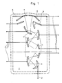
- the structure of a micro-secondary electron multiplier is shown schematically in Figure 1.
- the dynodes 1, the conductor tracks 2 attached to their voltage supply and the anode 3 can be seen. These structures are applied to the base plate 4.
- a second plate shown in dashed lines, carries a glass wall 6 on which the photocathode 7 is applied at a suitable point. Additional electrodes 8, 9 serve to focus the photoelectrons triggered on the photocathode onto the first dynode 1.
- the plates are connected to one another by glass soldering and, if necessary, form a vacuum-tight housing for the secondary electron multiplier.
- the multiplication requires electron energies of the order of magnitude 100 eV.
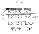
- FIG. 2a schematically shows a multiple arrangement of micro-secondary electron multipliers.
- numerous micro-secondary electron multipliers are arranged side by side and the routing of the conductor tracks 2 has been adapted accordingly.
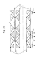
- 2b schematically shows a multiple arrangement with common dynodes 1.
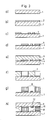
- 3a to 3h show an example of the production of a micro-secondary electron multiplier or a multiple arrangement (arrays), X-ray depth lithography with synchrotron radiation and electroforming being used as the most important process steps.
- a detailed description of these processes can be found in EW Becker, W. Ehrfeld, P. Hagmann, A. Maner and D Münchmeyer "Fabrication of Microstructures with high aspect ratio and great structural heights by synchrotron radiation lithography, galvanoforming, and plastic molding (LIGA-process ) ", Microelectronic Engineering 4 (1986) 35-36.
- 3a shows a base plate 1 made of aluminum oxide ceramic. The thickness of the base plate 1 is about 1 mm, the area is about 10 cm x 10 cm.
- the base plate 1 is spun with a thin layer 2 of photoresist (e.g. AZ 1350 Kalle, Wiesbaden) coated and pretreated according to the manufacturer's instructions (Fig. 3b).
- photoresist e.g. AZ 1350 Kalle, Wiesbaden
- the photoresist is irradiated and developed lithographically through a mask, so that a photoresist structure 3 is formed on the base plate 1 (FIG. 3c).
- a 30 nm thick layer 4 made of titanium and then another 200 nm thick layer made of nickel is deposited over the entire surface by means of a sputtering process.
- the photoresist 3 is then removed with acetone in the immersion bath, the regions of the metal layers 4 and 5 which are located on the photoresist structure 3 also being removed.
- a metal layer structure 4, 5 remains on the base plate 1 (FIG. 3d).
- a layer 6 of a polymethyl methacrylate casting compound (PMMA) is now poured on in a thickness of 1 mm, polymerized and then structured by means of deep X-ray lithography with synchrotron radiation and subsequent development (FIG. 3f).
- Nickel which represents the dynodes 8 of the micro-secondary electron multiplier, is electrodeposited into the PMMA shaped structure 7 thus produced.
- the remaining PMMA regions 7 are then removed in a solvent (FIG.
- the metal structure 10 is ver by diffusion soldering with silver with the dynodes 8 soldering, whereby the micro-secondary electron multiplier, consisting of a base plate 1, a cover plate 9, discrete dynodes 8, conductor tracks 11 for contacting the dynodes and conductor tracks 12 for the vertical focusing of the electrons, is completed (FIG. 3h).
- Another method for producing the microstructures is in the impression technique.
- X-ray lithography with synchrotron radiation is used to mold a positive of the dynode structure to be produced as a reusable tool with a plastic, whereupon the resulting negative shape is filled up by electrodeposition of metal and the remaining plastic is removed.
- the base plate required for fixing and contacting the dynodes is inserted into the mold during the molding process, so that the plastic forms a firm connection with the base plate.
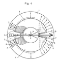
- a multi-channel scattered light radiometer (FIG. 4) is used as an application example.
- the scattering of light on small particles is an important aid in the investigation of size and shape parameters in particle systems (M. Kerker, The Scattering of Light, Academic Press, New York, 1969).
- One of the methods that provide the most information is measuring the angular distribution of the scattered light. Particularly cheap for the signal-to-noise ratio, the measurement time required and the time resolution is the simultaneous measurement of the scattered light at many different angles.
- the micro-secondary electron multiplier arrays according to the invention allow the construction of much smaller, more sensitive and robust electronic multichannel detectors than the state of the art (German Patent 23 38 481, US Patent 39 32762, German Utility Model G 8415886.7).
- the supply of the dynodes via conductor tracks allows the formation of groups of multi-channel micro-secondary electron multipliers, which can be connected to various voltage supplies.
- the sensitivity as a function of the scattering angle can be adapted to the scattered light angle distribution. This means, for example, that in the case of highly forward scattering particles, where the intensity difference between forward and backward can be several orders of magnitude, the rear detector area, about 90 ° -180 °, with the maximum gain, the middle area, about 20 ° -90 °, with a medium gain and the front area, 0 ° -20 °, can be driven just below the use of saturation effects.
- Two sector-shaped regions are provided with multiple arrangements (arrays) of microsecond electron multipliers 2 on an annular base plate 1.
- the inputs of the microsecond multiplier 2 are each arranged on an arc and point to the center of the base plate 1.
- the sector areas are each surrounded by a glass wall 3, which carries photocathodes on its inner arc. which are each assigned to a microsecond electron multiplier.
- the glass walls 3 are closed at the top with a cover plate 4, so that a vacuum-tight envelope of the multiple arrangements (arrays) is created.
- the signal outputs of the microsecond multiplier 2 are conducted with conductor tracks 5 to the outer edge of the base plate 1, where there are contacts 6 for external connection.
- the conductor tracks for supplying the multiple arrangements (arrays) are guided through metal-filled bores 7 to the underside of the base plate 1 and from there through conductor tracks 8 also to external connections 9 on the outer edge of the base plate 1.
- a semiconductor laser 10 In the free sectors of the base plate 1, a semiconductor laser 10, optical elements 11, diaphragms 12 and a wedge-shaped light sump 13 are arranged in such a way that a beam path suitable for the scattering of light due to density fluctuations of matter located in the scattering volume 14 is produced.
- the version shown in FIG. 4 makes it possible to check the symmetry of the scattered radiation with respect to the direction of the incident primary beam. This can be of considerable importance, e.g. for systems of non-symmetrical particles, which have been given an orientation by fluid dynamic or electromagnetic influence.
- the flat structure of such integrated measuring systems facilitates their use in several planes along a particle beam and thus the tracking of a temporal evolution of the particle parameters. It is also well suited for the application of a magnetic field for influencing the electron orbits.
- the application example used relates to light scattering, the scope also extends to scattering processes in which charged particles, such as electrons and ions, or excited neutrals are present, and also to radiation or particle sources which emit themselves.
Abstract
Description
Die Erfindung betrifft einen Sekundärelektronenvervielfacher nach dem Oberbegriff des Anspruches 1 sowie ein Verfahren zur Herstellung eines solchen Sekundärelektronenvervielfachers.The invention relates to a secondary electron multiplier according to the preamble of
Ein derartiger Sekundärelektronenvervielfacher ist aus der Firmendruckschrift SC-5 von Hamamatsu (Katalog 1983) unter der Typenbezeichnung R 1635 bekannt. Er besitzt bei acht Stufen einen Durchmesser von 10 mm und eine Länge von ca. 55mm. Diese Abmessungen erlauben nicht den Einsatz in miniaturisierten Meßsystemen.Such a secondary electron multiplier is known from the company publication SC-5 by Hamamatsu (catalog 1983) under the type designation R 1635. With eight steps, it has a diameter of 10 mm and a length of approx. 55 mm. These dimensions do not allow use in miniaturized measuring systems.
Bekannt sind auch Mikro-Kanalplatten (Nuclear Instruments und Methods 162, 587-601 (1979)). Sie erfüllen zwar die Anforderung des kleinen Raumbedarfs, weisen jedoch eine erhebliche Totzeit nach einem Signalimpuls auf, wodurch ihre Anwendbarkeit auf sehr schwache Strahlungs- und Teilchensignale beschränkt bleibt.Micro-channel plates (Nuclear Instruments and Methods 162, 587-601 (1979)) are also known. Although they meet the requirement for small space requirements, they have a considerable dead time after a signal pulse, which limits their applicability to very weak radiation and particle signals.
Weiterhin sind auch geschichtete Kanalplatten bekannt (Advances in Electronics and Electron Physics 33A, 117-123 (1972)). Sie vermeiden zwar den Nachteil einer langen Totzeit, weisen jedoch von Stufe zu Stufe erhebliche Elektronenverluste auf, wodurch sie wiederum für Anwendungen mit extrem kleinen Strahlungs- oder Teilchensignalen ungeeignet sind. Weiterhin sind geschichtete Kanalplatten bekannt (DE 24 14 658), bei denen solche Verluste durch Formung der Kanalwände mittels Ätzen verkleinert werden sollen, jedoch sind dieser Art von Formgebung enge Grenzen gesetzt. Schließlich sind aus der Hochenergiephysik Arrays von Sekundärelektronenvervielfachern bekannt (F. Binon et al, Nuclear Instruments and Methods, A248 (1986), 86 - 102). Durch ihren großen Platzbedarf sind sie für den Aufbau miniaturisierter Meßsysteme vollständig ungeeignet.Layered channel plates are also known (Advances in Electronics and Electron Physics 33A, 117-123 (1972)). Although they avoid the disadvantage of a long dead time, they have considerable electron losses from stage to stage, which in turn makes them unsuitable for applications with extremely small radiation or particle signals. Layered duct plates are also known (DE 24 14 658), in which such losses occur by forming the duct walls by means of etching should be reduced in size, but this type of design has narrow limits. Finally, arrays of secondary electron multipliers are known from high energy physics (F. Binon et al, Nuclear Instruments and Methods, A248 (1986), 86-102). Due to their large space requirement, they are completely unsuitable for the construction of miniaturized measuring systems.
Der Erfindung liegt die Aufgabe zugrunde, gegenüber dem aufgezeigten Stand der Technik einen Mikro-Sekundärelektronenvervielfacher und Arrays davon zu schaffen, die einen äußerst geringen Platzbedarf, eine hohe Zeitauflösung, eine große Empfindlichkeit und eine hohe Flexibilität bei der Formgebung aufweisen.The object of the invention is to create a micro-secondary electron multiplier and arrays thereof compared to the prior art shown, which have an extremely small space requirement, a high time resolution, a high sensitivity and a high flexibility in the shaping.
Diese Aufgabe wird erfindungsgemäß mittels der in kennzeichnenden Teil des Anspruches 1 angegebenen Merkmals und dem Verfahren nach Anspruch 11 gelöst.This object is achieved by means of the feature specified in the characterizing part of
Die übrigen Ansprüche 2 bis 10 sowie die Ansprüche 12 bis 17 geben vorteilhafte Weiterbildungen und Ausführungsformen des erfindungsgemäßen Gegenstandes bzw. des Verfahrens an.The
Die erfindungsgemäßen Mikro-Sekundärelektronenvervielfacher und Vielfachanordnungen (Arrays) davon als Sensoren in miniaturisierten Meßsystemen für Strahlung oder Teilchen zeichnen sich in vorteilhafter Weise durch geringen Raumbedarf sowie hohe Orts- und Zeitauflösung aus.The micro-secondary electron multiplier and multiple arrangements (arrays) thereof as sensors in miniaturized measuring systems for radiation or particles are advantageously characterized by a small space requirement and high spatial and time resolution.
Durch Einsatz von Röntgentiefenlithographie und Mikrogalvanik wird der Aufbau eines extrem kleinen Systems von diskreten Dynoden ermöglicht, deren Form so gewählt ist, daß die Elektronen von einer Dynode auf die nächste fokussiert und Elektronenverluste so minimiert werden. Die Empfindlichkeit wird dadurch vorteilhaft beeinflußt. Die Spannungsversorgung der Dynoden über diskrete Leiterbahnen gestattet es, die externe Versorgung an die Signalamplitude anzupassen, so daß der dynamische Bereich des Mikro-Sekundärelektronenvervielfachers sehr groß wird. Durch die stark reduzierte Länge des Sekundärelektronenvervielfachers ist die Elektronenlaufzeit von Kathode zu Anode verkürzt, was sich günstig auf die Anstiegszeit von Impulsen und damit auf die erzielbare Zeitauflösung auswirkt.The use of deep X-ray lithography and micro-electroplating enables the construction of an extremely small system of discrete dynodes, the shape of which is selected in such a way that the electrons are focused from one dynode to the next, thus minimizing electron losses. The sensitivity is advantageously influenced. The supply of power to the dynodes via discrete conductor tracks allows the external supply to be matched to the signal amplitude, so that the dynamic range of the micro-secondary electron multiplier becomes very large. The greatly reduced length of the secondary electron multiplier shortens the electron transit time from cathode to anode, which has a favorable effect on the rise time of pulses and thus on the achievable time resolution.
Die Herstellung derart feiner Strukturen auf röntgentiefenlithographisch-galvanoplastischem Wege (LIGA-Technik) bzw. durch die hiervon abgeleitete Abformtechnik gemäß Merkmal b) von Patentanspruch 13 ist u.a. in dem KfK-Bericht 3995 des Kernforschungszentrums Karlsruhe (November 1985) beschrieben und dargestellt. Danach wird z.B. ein röntgenstrahlenempfindlicher Positiv-Resist auf eine metallische Grundplatte aufgebracht und partiell über eine Maske mit Röntgenstrahlen so bestrahlt und entwickelt, daß eine Negativform der herzustellenden Stege entsteht, deren Höhe der Schichtdicke des Positiv-Resist entspricht; sie kann bis zu 2 mm betragen, je nach der Eindringtiefe der Röntgenstrahlung. Anschließend wird die Negativform galvanisch mit einem Metall unter Verwendung der Grundplatte als Elektrode aufgefüllt, worauf das rest liche Resist-Material mit einem Lösungsmittel entfernt wird. Bei der Abformtechnik wird ein mit der LIGA-Technik hergestelltes Positiv der herzustellenden Steg-Struktur als wiederholt verwendbares Werkzeug mit einem Kunststoff abgeformt, worauf die so entstandene Negativform durch galvanisches Abscheiden von Metall aufgefüllt und der restliche Kunststoff entfernt wird. In beiden Fällen lassen sich extrem genaue und feine Strukturen herstellen mit lateralen Abmessungen im µm-Bereich bei einer frei wählbaren Höhe bis zu ca. 2mm. Bei etwas geringeren Höhen lassen sich auch minimale laterale Abmessungen im Submikrometerbereich realisieren. Als Strahlenquelle für diesen Zweck ist insbesondere die Röntgenstrahlung eines Elektronen-Synchrotrons oder -Speicherrings (Synchrotronstrahlung) geeignet.The production of such fine structures by X-ray lithography-galvanoplastic (LIGA technology) or by means of the impression technique derived therefrom according to feature b) of
Durch das im Anspruch 13 beschriebene Verfahren ist es weiterhin möglich, eine große Anzahl von Mikro-Sekundärelektronenvervielfachern nebeneinander auf derselben Grundplatte als Mikro-Sekundärelektronenvervielfacher-Array aufzubauen. Dadurch wird eine extrem hohe Packungsdichte erreicht, die sich günstig auf das erreichbare räumliche Auflösungsvermögen auswirkt, ein Aspekt, der insbesondere für die Tomographie und für Detektoren in der Hochenergiephysik von Bedeutung ist.The method described in
Bei einem Array von Mikro-Sekundärelektronenvervielfachern kann die Position der Signal-Eingänge an vorgegebene Konturen angepaßt werden, z.B. an den Rowland-Kreis, an eine gewölbte Bildfläche oder an einen Zylin dermantel wie beim nachstehend als Ausführungsbeispiel beschriebenen Streulichtradiometer.In the case of an array of micro secondary electron multipliers, the position of the signal inputs can be adapted to predetermined contours, for example to the Rowland circle, to an arched image area or to a cylinder the jacket as in the scattered light radiometer described below as an exemplary embodiment.
Ein weiterer Vorteil liegt darin, daß eine der Substratplatten mit einer lichtdurchlässigen Wand, die zusätzlich noch Photokathoden trägt, versehen werden und damit der Mikro-Sekundärelektronenvervielfacher (-Array) zu einem Mikro-Photomultiplier(-Array) gemacht werden kann.Another advantage is that one of the substrate plates is provided with a translucent wall, which also carries photocathodes, and thus the micro-secondary electron multiplier (array) can be made into a micro-photomultiplier (array).
Gibt man der lichtdurchlässigen Wand einen linsenförmigen Querschnitt und bringt die Photokathoden auf einem getrennten Träger aus lichtdurchlässigem Material an, so kann man zwischen Lichtquelle und Photokathode eine optische Abbildung herstellen, die sich vorteilhaft auswirkt auf die Definition des Streuvolumens und auf das Signal-Rausch-Verhältnis.If you give the translucent wall a lenticular cross-section and attach the photocathodes on a separate support made of translucent material, you can create an optical image between the light source and photocathode, which has an advantageous effect on the definition of the scattering volume and on the signal-to-noise ratio .
Der Aufbau eines Mikro-Sekundärelektronenvervielfachers ist schematisch in Figur 1 dargestellt. Man erkennt die Dynoden 1, die zu ihrer Spannungsversorgung angebrachten Leiterbahnen 2 sowie die Anode 3. Diese Strukturen sind auf der Grundplatte 4 aufgebracht. Eine zweite Platte trägt, gestrichelt dargestellt, eine Glaswand 6, auf der an geeigneter Stelle die Photokathode 7 aufgebracht ist. Weitere Elektroden 8, 9 dienen der Fokussierung der auf der Photokathode ausgelösten Photoelektronen auf die erste Dynode 1. Die Platten werden durch Glaslöten miteinander verbunden und bilden, falls erforderlich, ein vakuumdichtes Gehäuse für den Sekundärelektronenvervielfacher. Die Vervielfachung erfordert Elektronenenergien von der Größenord nung 100 eV. Mit einem typischen sicheren Betriebswert für die Oberflächenfeldstärke von 1 kV/mm ergibt sich ein minimaler Leiterbahnabstand von 0,1 mm und bei 9 Dynoden mit einer Kantenlänge von je 1 mm eine Gesamtlänge von ca. 10 mm. Oberflächenaufladung und daraus folgende elektrische Überschläge werden durch die, wenn auch schwache, Leitfähigkeit der Oberflächenschicht der Wände vermieden.The structure of a micro-secondary electron multiplier is shown schematically in Figure 1. The
Figur 2a zeigt schematisch eine Vielfachanordnung von Mikro-Sekundärelektronenvervielfachern. Hier sind zahlreiche Mikro-Sekundärelektronenvervielfacher nebeneinander angeordnet und die Führung der Leiterbahnen 2 entsprechend angepaßt worden. Fig. 2b zeigt schematisch eine Vielfachanordnung mit gemeinsamen Dynoden 1.FIG. 2a schematically shows a multiple arrangement of micro-secondary electron multipliers. Here numerous micro-secondary electron multipliers are arranged side by side and the routing of the
Fig. 3a bis 3h zeigt beispielhaft die Herstellung eines Mikro-Sekundärelektronenvervielfachers oder einer Vielfachanordnung (Arrays), wobei als wichtigste Verfahrensschritte Röntgentiefenlithographie mit Synchrotronstrahlung und Galvanoformung eingesetzt werden. Eine detaillierte Beschreibung dieser Prozesse ist in E.W. Becker, W. Ehrfeld, P. Hagmann, A. Maner und D Münchmeyer "Fabrication of Microstructures with high aspect ratio and great structural heights by synchrotron radiation lithography, galvanoforming, and plastic moulding (LIGA-process)", Microelectronic Engineering 4 (1986) 35-36 angegeben. Fig. 3a zeigt eine Grundplatte 1 aus Aluminiumoxid-Keramik. Die Dicke der Grundplatte 1 beträgt etwa 1 mm, die Fläche etwa 10 cm x 10 cm. Die Grundplatte 1 wird durch Aufschleudern mit einer dünnen Schicht 2 aus Fotolack (z.B.AZ 1350 der Fa. Kalle, Wiesbaden) beschichtet und nach Herstellerangaben vorbehandelt (Fig. 3b). In bekannter Weise wird der Fotolack über eine Maske lithographisch bestrahlt und entwickelt, so daß eine Fotolackstruktur 3 auf der Grundplatte 1 entsteht (Fig. 3c). Anschließend wird durch einen Sputterprozeß ganzflächig zunächst eine 30 nm dicke Schicht 4 aus Titan und dann eine weitere 200 nm dicke Schicht aus Nickel abgeschieden. Sodann wird der Fotolack 3 mit Aceton im Tauchbad entfernt, wobei auch die Bereiche der Metallschichten 4 und 5 entfernt werden, die sich auf der Fotolackstruktur 3 befinden. Es verbleibt eine Metallschichtstruktur 4, 5 auf der Grundplatte 1 (Fig. 3d). Wie im o.g. Artikel beschrieben, wird nun in einer Dicke von 1 mm eine Schicht 6 aus einer Polymethylmethacrylat-Gießmasse (PMMA) aufgegossen, polymerisiert und dann mittels Röntgentiefenlithographie mit Synchrotronstrahlung und anschließendes Entwickeln strukturiert (Fig. 3f). In die so gefertigte Formstruktur 7 aus PMMA wird galvanisch Nickel abgeschieden, das die Dynoden 8 des Mikro-Sekundärelektronenvervielfachers darstellt. Anschließend werden die verbliebenen PMMA-Bereiche 7 in einem Lösemittel entfernt (Fig. 3g). In gleicher Weise werden in denselben Arbeitsschritten durch Vorgabe entsprechender Strukturen auf den in den Lithographieprozessen verwendeten Masken andere Elemente des Mikro-Sekundärelektronenvervielfachers wie etwa Anoden, Abschirmungen und dergleichen parallel mit den Dynoden 8 gefertigt. Analog zu den Prozess-Schritten in Fig. 3a bis 3d wird nun eine zur Grundplatte in Fig. 3d spiegelsymmetrische Deckplatte 9 mit Metallstrukturen 10 hergestellt. Die Metallstruktur 10 wird durch Diffusionslöten mit Silber mit den Dynoden 8 ver lötet, wodurch der Mikro-Sekundärelektronenvervielfacher, bestehend aus einer Grundplatte 1, einer Deckplatte 9, diskreten Dynoden 8, Leiterbahnen 11 zur Kontaktierung der Dynoden und Leiterbahnen 12 für die vertikale Fokussierung der Elektronen, fertiggestellt wird (Fig. 3h).3a to 3h show an example of the production of a micro-secondary electron multiplier or a multiple arrangement (arrays), X-ray depth lithography with synchrotron radiation and electroforming being used as the most important process steps. A detailed description of these processes can be found in EW Becker, W. Ehrfeld, P. Hagmann, A. Maner and D Münchmeyer "Fabrication of Microstructures with high aspect ratio and great structural heights by synchrotron radiation lithography, galvanoforming, and plastic molding (LIGA-process ) ", Microelectronic Engineering 4 (1986) 35-36. 3a shows a
Eine weitere Methode zur Herstellung der Mikrostrukturen besteht in der Abformtechnik. Dabei wird durch Röntgentiefenlithographie mit Synchrotronstrahlung eine Positiv der herzustellenden Dynodenstruktur als wiederholt verwendbares Werkzeug mit einem Kunststoff abgeformt, worauf die entstandene Negativform durch galvanisches Abscheiden von Metall aufgefüllt und der restliche Kunststoff entfernt wird. Die für die Fixierung und Kontaktierung der Dynoden erforderliche Grundplatte wird beim Abformprozess in das Werkzeug eingelegt, so daß der Kunststoff mit der Grundplatte eine feste Verbindung eingeht. Sowohl die direkte Herstellung der Mikrostrukturen durch Röntgentiefenlithographie mit Synchrotronstrahlung als auch die Abformtechnik ermöglichen extreme Strukturgenauigkeiten mit Lateralabmessungen im µm-Bereich bei einer frei wählbaren Höhe bis zu ca 2mm.Another method for producing the microstructures is in the impression technique. X-ray lithography with synchrotron radiation is used to mold a positive of the dynode structure to be produced as a reusable tool with a plastic, whereupon the resulting negative shape is filled up by electrodeposition of metal and the remaining plastic is removed. The base plate required for fixing and contacting the dynodes is inserted into the mold during the molding process, so that the plastic forms a firm connection with the base plate. Both the direct production of the microstructures by means of deep x-ray lithography with synchrotron radiation and the impression technique enable extreme structural accuracy with lateral dimensions in the µm range with a freely selectable height of up to approx. 2mm.
Als Anwendungsbeispiel wird ein Vielkanal-Streulichtradiometer (Fig. 4) herangezogen. Bekanntlich ist die Streuung von Licht an kleinen Teilchen ein wichtiges Hilfsmittel bei der Untersuchung von Größen- und Formparametern in Teilchensystemen (M. Kerker, The Scattering of Light, Academic Press, New York, 1969). Eine der Methoden, die am meisten Information liefern, ist die Messung der Winkelverteilung des gestreuten Lichts. Besonders günstig für das Signal-Rausch-Verhältnis, die benötigte Meßzeit und die Zeitauflösung ist die simultane Messung des Streulichts unter vielen, verschiedenen Winkeln. Die erfindungsgemäßen Mikro-Sekundärelektronenvervielfacher-Arrays erlauben den Aufbau wesentlich kleinerer, empfindlicherer und robusterer elektronischer Vielkanaldetektoren als es dem Stand der Technik entspricht (Deutsches Patent 23 38 481, US-Patent 39 32762, Deutsches Gebrauchsmuster G 8415886,7). Die Versorgung der Dynoden über Leiterbahnen erlaubt die Bildung von Gruppen von Vielkanal-Mikro-Sekundärelektronenvervielfachern, die an verschiedene Spannungsversorgungen angeschlossen werden können. Dadurch kann die Empfindlichkeit als Funktion des Streuwinkels der Streulicht-Winkelverteilung angepaßt werden. Dies bedeutet beispielsweise, daß im Falle von stark vorwärts streuenden Teilchen, wo der Intensitätsunterschied zwischen vorwärts und rückwärts mehrere Großenordnungen betragen kann, der hintere Detektorbereich, etwa 90°-180°, mit der maximalen Verstärkung, der mittlere Bereich, etwa 20°-90°, mit einer mittleren Verstärkung und der vordere Bereich, 0°-20°, gerade unterhalb des Einsatzes von Sättigungseffekten gefahren werden können.A multi-channel scattered light radiometer (FIG. 4) is used as an application example. As is known, the scattering of light on small particles is an important aid in the investigation of size and shape parameters in particle systems (M. Kerker, The Scattering of Light, Academic Press, New York, 1969). One of the methods that provide the most information is measuring the angular distribution of the scattered light. Particularly cheap for the signal-to-noise ratio, the measurement time required and the time resolution is the simultaneous measurement of the scattered light at many different angles. The micro-secondary electron multiplier arrays according to the invention allow the construction of much smaller, more sensitive and robust electronic multichannel detectors than the state of the art (German Patent 23 38 481, US Patent 39 32762, German Utility Model G 8415886.7). The supply of the dynodes via conductor tracks allows the formation of groups of multi-channel micro-secondary electron multipliers, which can be connected to various voltage supplies. As a result, the sensitivity as a function of the scattering angle can be adapted to the scattered light angle distribution. This means, for example, that in the case of highly forward scattering particles, where the intensity difference between forward and backward can be several orders of magnitude, the rear detector area, about 90 ° -180 °, with the maximum gain, the middle area, about 20 ° -90 °, with a medium gain and the front area, 0 ° -20 °, can be driven just below the use of saturation effects.
Auf einer ringförmigen Grundplatte 1 werden zwei sektorförmige Gebiete mit Vielfachanordnungen (Arrays) von Mikrosekundärelektronenvervielfachern 2 versehen. Die Eingänge der Mikrosekundärelektronenvervielfacher 2 sind dabei auf je einem Kreisbogen angeordnet und weisen zum Mittelpunkt der Grundplatte 1. Die Sektor-Gebiete werden von je einer Glaswand 3 umschlossen, die auf ihrem inneren Bogen Photokathoden trägt. die jeweils einem Mikrosekundärelektronenvervielfacher zugeordnet sind.Two sector-shaped regions are provided with multiple arrangements (arrays) of
Die Glaswände 3 sind mit je einer Deckelplatte 4 nach oben verschlossen, so daß eine vakuumdichte Umhüllung der Vielfachanordnungen (Arrays) entsteht. Die Signalausgänge der Mikrosekundärelektronenvervielfacher 2 werden mit Leiterbahnen 5 zum äußeren Rand der Grundplatte 1 geführt, wo sich Kontakte 6 zum externen Anschluß befinden. Die Leiterbahnen zur Versorgung der Vielfachanordnungen (Arrays) werden durch metallgefüllte Bohrungen 7 zur Unterseite der Grundplatte 1 und von da durch Leiterbahnen 8 ebenfalls zu externen Anschlüssen 9 am Außenrand der Grundplatte 1 geführt. In den freien Sektoren der Grundplatte 1 werden ein Halbleiterlaser 10, optische Elemente 11, Blenden 12 und ein keilförmiger Lichtsumpf 13 derart angeordnet, daß ein für die Streuuung von Licht an Dichtefluktuationen von Materie, die sich im Streuvolumen 14 befindet, geeigneter Strahlengang entsteht.The
Die in Fig. 4 gezeigte Version macht es möglich, die Symmetrie der Streustrahlung bezüglich der Richtung des einfallenden Primärstrahles zu prüfen. Dies kann von erheblicher Bedeutung sein, z.B. für Systeme nichtsymmetrischer Teilchen, denen durch fluiddynamische oder elektromagnetische Einwirkung eine Orientierung aufgeprägt wurde.The version shown in FIG. 4 makes it possible to check the symmetry of the scattered radiation with respect to the direction of the incident primary beam. This can be of considerable importance, e.g. for systems of non-symmetrical particles, which have been given an orientation by fluid dynamic or electromagnetic influence.
Der flache Aufbau solcher integrierter Meßsysteme erleichtert ihren Einsatz in mehreren Ebenen längs eines Teilchenstrahls und damit die Verfolgung einer zeitlichen Evolution der Teilchenparameter. Er eignet sich darüberhinaus gut für die Anwendung eines Magnetfeldes zur Beeinflussung der Elektronenbahnen. Obwohl das herangezogene Anwendungsbeispiel sich auf die Lichtstreuung bezieht, erstreckt sich der Anwendungsbereich auch auf Streuprozesse, bei denen geladene Teilchen, wie Elektronen und Ionen, oder angeregte Neutrale vorliegen, und darüber hinaus auch auf Strahlungs- oder Teilchenquellen, die selbst emittieren.The flat structure of such integrated measuring systems facilitates their use in several planes along a particle beam and thus the tracking of a temporal evolution of the particle parameters. It is also well suited for the application of a magnetic field for influencing the electron orbits. Although the application example used relates to light scattering, the scope also extends to scattering processes in which charged particles, such as electrons and ions, or excited neutrals are present, and also to radiation or particle sources which emit themselves.
Claims (16)
Priority Applications (1)
| Application Number | Priority Date | Filing Date | Title |
|---|---|---|---|
| AT88103116T ATE76537T1 (en) | 1987-03-20 | 1988-03-02 | MICRO-SECONDARY ELECTRON MULTIPLE AND METHOD FOR ITS MANUFACTURE. |
Applications Claiming Priority (2)
| Application Number | Priority Date | Filing Date | Title |
|---|---|---|---|
| DE3709298 | 1987-03-20 | ||
| DE19873709298 DE3709298A1 (en) | 1987-03-20 | 1987-03-20 | MICRO SECONDARY ELECTRONIC MULTIPLIER AND METHOD FOR THE PRODUCTION THEREOF |
Publications (3)
| Publication Number | Publication Date |
|---|---|
| EP0283773A2 true EP0283773A2 (en) | 1988-09-28 |
| EP0283773A3 EP0283773A3 (en) | 1990-02-07 |
| EP0283773B1 EP0283773B1 (en) | 1992-05-20 |
Family
ID=6323660
Family Applications (1)
| Application Number | Title | Priority Date | Filing Date |
|---|---|---|---|
| EP88103116A Expired - Lifetime EP0283773B1 (en) | 1987-03-20 | 1988-03-02 | Miniaturized secondary electron multiplier and its manufacturing procedure |
Country Status (5)
| Country | Link |
|---|---|
| US (1) | US4990827A (en) |
| EP (1) | EP0283773B1 (en) |
| JP (1) | JPS63279553A (en) |
| AT (1) | ATE76537T1 (en) |
| DE (1) | DE3709298A1 (en) |
Cited By (1)
| Publication number | Priority date | Publication date | Assignee | Title |
|---|---|---|---|---|
| EP0515261A1 (en) * | 1991-05-21 | 1992-11-25 | Commissariat A L'energie Atomique | Ceramic electron multiplying structure especially for photomultiplier and its manufacturing procedure |
Families Citing this family (15)
| Publication number | Priority date | Publication date | Assignee | Title |
|---|---|---|---|---|
| US5077504A (en) * | 1990-11-19 | 1991-12-31 | Burle Technologies, Inc. | Multiple section photomultiplier tube |
| US5545367A (en) * | 1992-04-15 | 1996-08-13 | Soane Technologies, Inc. | Rapid prototype three dimensional stereolithography |
| US5264693A (en) * | 1992-07-01 | 1993-11-23 | The United States Of America As Represented By The Secretary Of The Navy | Microelectronic photomultiplier device with integrated circuitry |
| US5412265A (en) * | 1993-04-05 | 1995-05-02 | Ford Motor Company | Planar micro-motor and method of fabrication |
| US5656807A (en) * | 1995-09-22 | 1997-08-12 | Packard; Lyle E. | 360 degrees surround photon detector/electron multiplier with cylindrical photocathode defining an internal detection chamber |
| WO1998019341A1 (en) | 1996-10-30 | 1998-05-07 | Nanosystems, Inc. | Microdynode integrated electron multiplier |
| US6115634A (en) * | 1997-04-30 | 2000-09-05 | Medtronic, Inc. | Implantable medical device and method of manufacture |
| US5943223A (en) * | 1997-10-15 | 1999-08-24 | Reliance Electric Industrial Company | Electric switches for reducing on-state power loss |
| EP1445670A1 (en) | 2003-02-06 | 2004-08-11 | ETA SA Manufacture Horlogère Suisse | Balance-spring resonator spiral and its method of fabrication |
| GB2409927B (en) * | 2004-01-09 | 2006-09-27 | Microsaic Systems Ltd | Micro-engineered electron multipliers |
| US7317283B2 (en) * | 2005-03-31 | 2008-01-08 | Hamamatsu Photonics K.K. | Photomultiplier |
| US7397184B2 (en) * | 2005-03-31 | 2008-07-08 | Hamamatsu Photonics K.K. | Photomultiplier |
| US7427835B2 (en) * | 2005-03-31 | 2008-09-23 | Hamamatsu Photonics K.K. | Photomultiplier including a photocathode, a dynode unit, a focusing electrode, and an accelerating electrode |
| EP1818736A1 (en) * | 2006-02-09 | 2007-08-15 | The Swatch Group Research and Development Ltd. | Shockproof collet |
| DE102015200739B3 (en) * | 2015-01-19 | 2016-03-24 | Fraunhofer-Gesellschaft zur Förderung der angewandten Forschung e.V. | CIRCUIT ACCUMULATOR FOR ACCELERATING CHARGING SUPPLEMENTS AND METHOD FOR PRODUCING A CIRCUIT ACCUMULATOR |
Citations (2)
| Publication number | Priority date | Publication date | Assignee | Title |
|---|---|---|---|---|
| US2674661A (en) * | 1948-08-12 | 1954-04-06 | Rca Corp | Electron multiplier device |
| US4034255A (en) * | 1975-11-28 | 1977-07-05 | Rca Corporation | Vane structure for a flat image display device |
Family Cites Families (12)
| Publication number | Priority date | Publication date | Assignee | Title |
|---|---|---|---|---|
| US2836760A (en) * | 1955-03-08 | 1958-05-27 | Egyesuelt Izzolampa | Electron multiplier |
| US2868994A (en) * | 1955-10-24 | 1959-01-13 | Rca Corp | Electron multiplier |
| US4041343A (en) * | 1963-07-12 | 1977-08-09 | International Telephone And Telegraph Corporation | Electron multiplier mosaic |
| US3551841A (en) * | 1967-01-30 | 1970-12-29 | Philips Corp | Thin film laser device employing an optical cavity |
| FR2000354A1 (en) * | 1968-01-18 | 1969-09-05 | Matsushita Electric Ind Co Ltd | |
| GB1434053A (en) * | 1973-04-06 | 1976-04-28 | Mullard Ltd | Electron multipliers |
| DE2338481C2 (en) * | 1973-07-28 | 1985-07-04 | Kernforschungszentrum Karlsruhe Gmbh, 7500 Karlsruhe | Device for rapid measurement of the change in radiation intensity over time |
| FR2445018A1 (en) * | 1978-12-22 | 1980-07-18 | Anvar | ELECTRON MULTIPLIER TUBE WITH AXIAL MAGNETIC FIELD |
| JPS6042573B2 (en) * | 1979-01-24 | 1985-09-24 | 浜松ホトニクス株式会社 | Secondary electron multiplier electrode |
| JPS5856781B2 (en) * | 1980-07-07 | 1983-12-16 | 日景 ミキ子 | Screw fastening method using intermediary material |
| FR2549288B1 (en) * | 1983-07-11 | 1985-10-25 | Hyperelec | ELECTRON MULTIPLIER ELEMENT, ELECTRON MULTIPLIER DEVICE COMPRISING THE MULTIPLIER ELEMENT AND APPLICATION TO A PHOTOMULTIPLIER TUBE |
| DE8415886U1 (en) * | 1984-05-24 | 1984-08-23 | Kernforschungszentrum Karlsruhe Gmbh, 7500 Karlsruhe | DEVICE FOR QUICKLY MEASURING THE RADIATION INTENSITY |
-
1987
- 1987-03-20 DE DE19873709298 patent/DE3709298A1/en active Granted
-
1988
- 1988-03-02 AT AT88103116T patent/ATE76537T1/en not_active IP Right Cessation
- 1988-03-02 EP EP88103116A patent/EP0283773B1/en not_active Expired - Lifetime
- 1988-03-17 JP JP63062080A patent/JPS63279553A/en active Pending
- 1988-03-17 US US07/169,607 patent/US4990827A/en not_active Expired - Fee Related
Patent Citations (2)
| Publication number | Priority date | Publication date | Assignee | Title |
|---|---|---|---|---|
| US2674661A (en) * | 1948-08-12 | 1954-04-06 | Rca Corp | Electron multiplier device |
| US4034255A (en) * | 1975-11-28 | 1977-07-05 | Rca Corporation | Vane structure for a flat image display device |
Non-Patent Citations (1)
| Title |
|---|
| IEEE TRANSACTIONS ON NUCLEAR SCIENCE, Band NS-32, Nr. 6, Dezember 1985, Seiten 3996-4000, IEEE, New York, US; D.K. LYNN et al.: "Thermionic integrated circuits: electronics for hostile environments" * |
Cited By (3)
| Publication number | Priority date | Publication date | Assignee | Title |
|---|---|---|---|---|
| EP0515261A1 (en) * | 1991-05-21 | 1992-11-25 | Commissariat A L'energie Atomique | Ceramic electron multiplying structure especially for photomultiplier and its manufacturing procedure |
| FR2676862A1 (en) * | 1991-05-21 | 1992-11-27 | Commissariat Energie Atomique | MULTIPLICATOR STRUCTURE OF ELECTRONS IN CERAMIC PARTICULARLY FOR PHOTOMULTIPLIER AND METHOD OF MANUFACTURING THE SAME |
| US5367218A (en) * | 1991-05-21 | 1994-11-22 | Commissariat A L'energie Atomique | Ceramic electron multiplying structure, particularly for a photomultiplier and its production process |
Also Published As
| Publication number | Publication date |
|---|---|
| DE3709298C2 (en) | 1990-02-08 |
| EP0283773A3 (en) | 1990-02-07 |
| JPS63279553A (en) | 1988-11-16 |
| ATE76537T1 (en) | 1992-06-15 |
| DE3709298A1 (en) | 1988-09-29 |
| US4990827A (en) | 1991-02-05 |
| EP0283773B1 (en) | 1992-05-20 |
Similar Documents
| Publication | Publication Date | Title |
|---|---|---|
| EP0283773B1 (en) | Miniaturized secondary electron multiplier and its manufacturing procedure | |
| EP0547371B1 (en) | Process for producing stepped moulds | |
| DE102005040267B4 (en) | Method for producing a multilayer electrostatic lens arrangement, in particular a phase plate and such a phase plate | |
| DE60312180T2 (en) | MONOLITATED MINIATURIZED MASS SPECTROMETER | |
| DE4024275A1 (en) | METHOD FOR THE PRODUCTION OF MICROSTRUCTURES WITH AREAS OF DIFFERENT STRUCTURAL HEIGHT | |
| DE2453772A1 (en) | FAST SPEED CAMERA FOR IMAGE CONVERTER TUBES | |
| DE3842354C2 (en) | ||
| DE1089895B (en) | Electronic image amplifier | |
| DE3909449C2 (en) | ||
| EP0154796B1 (en) | Manufacturing process for layered metallic multichannel plates for an image intensifier, and use of plates so manufactured | |
| DE3704716A1 (en) | LOCALLY SENSITIVE DETECTOR | |
| EP0618502B1 (en) | Process for making stepped moulds, stepped moulds and high precision stepped microstructure bodies moulded therewith | |
| US4563250A (en) | Method for producing multichannel plates | |
| DE2416186B2 (en) | MASK FOR STRUCTURING THIN LAYERS | |
| DE2448793C3 (en) | Electronic image intensifier or image converter tubes and methods for their manufacture | |
| DE2811382A1 (en) | ROENTGEN DETECTOR | |
| DE2448793B2 (en) | Electronic image intensifier or image converter tubes and methods for their manufacture | |
| DE202004002189U1 (en) | ion detector | |
| EP0603844A1 (en) | Microminiaturized electrostatic pump and method of production thereof | |
| DE1598130C3 (en) | Method and device for material analysis in a secondary electron emission microscope | |
| DE1037610B (en) | Electron multiplier with a large number of dynodes arranged between the cathode and the fluorescent screen, in which the carriers of the secondary electron emission layers are grid-like structures | |
| DE2423928A1 (en) | METHOD OF RECORDING ELECTROSTATIC CHARGE IMAGES | |
| DE2401662A1 (en) | ELECTRON MULTIPLE | |
| DE112020006001T5 (en) | CHARGED DETECTOR, CHARGED RADIATION DEVICE, RADIATION DETECTOR AND RADIATION DETECTION DEVICE | |
| EP1565764B1 (en) | Locally sensitive measuring device |
Legal Events
| Date | Code | Title | Description |
|---|---|---|---|
| PUAI | Public reference made under article 153(3) epc to a published international application that has entered the european phase |
Free format text: ORIGINAL CODE: 0009012 |
|
| AK | Designated contracting states |
Kind code of ref document: A2 Designated state(s): AT CH FR GB IT LI NL SE |
|
| PUAL | Search report despatched |
Free format text: ORIGINAL CODE: 0009013 |
|
| AK | Designated contracting states |
Kind code of ref document: A3 Designated state(s): AT CH FR GB IT LI NL SE |
|
| 17P | Request for examination filed |
Effective date: 19900131 |
|
| 17Q | First examination report despatched |
Effective date: 19911002 |
|
| GRAA | (expected) grant |
Free format text: ORIGINAL CODE: 0009210 |
|
| AK | Designated contracting states |
Kind code of ref document: B1 Designated state(s): AT CH FR GB IT LI NL SE |
|
| PG25 | Lapsed in a contracting state [announced via postgrant information from national office to epo] |
Ref country code: IT Free format text: LAPSE BECAUSE OF FAILURE TO SUBMIT A TRANSLATION OF THE DESCRIPTION OR TO PAY THE FEE WITHIN THE PRESCRIBED TIME-LIMIT;WARNING: LAPSES OF ITALIAN PATENTS WITH EFFECTIVE DATE BEFORE 2007 MAY HAVE OCCURRED AT ANY TIME BEFORE 2007. THE CORRECT EFFECTIVE DATE MAY BE DIFFERENT FROM THE ONE RECORDED. Effective date: 19920520 Ref country code: SE Effective date: 19920520 |
|
| REF | Corresponds to: |
Ref document number: 76537 Country of ref document: AT Date of ref document: 19920615 Kind code of ref document: T |
|
| ET | Fr: translation filed | ||
| GBT | Gb: translation of ep patent filed (gb section 77(6)(a)/1977) | ||
| PG25 | Lapsed in a contracting state [announced via postgrant information from national office to epo] |
Ref country code: AT Effective date: 19930302 |
|
| PLBE | No opposition filed within time limit |
Free format text: ORIGINAL CODE: 0009261 |
|
| STAA | Information on the status of an ep patent application or granted ep patent |
Free format text: STATUS: NO OPPOSITION FILED WITHIN TIME LIMIT |
|
| 26N | No opposition filed | ||
| PGFP | Annual fee paid to national office [announced via postgrant information from national office to epo] |
Ref country code: GB Payment date: 19940125 Year of fee payment: 7 |
|
| PGFP | Annual fee paid to national office [announced via postgrant information from national office to epo] |
Ref country code: CH Payment date: 19940127 Year of fee payment: 7 |
|
| PGFP | Annual fee paid to national office [announced via postgrant information from national office to epo] |
Ref country code: FR Payment date: 19940330 Year of fee payment: 7 |
|
| PGFP | Annual fee paid to national office [announced via postgrant information from national office to epo] |
Ref country code: NL Payment date: 19940331 Year of fee payment: 7 |
|
| PG25 | Lapsed in a contracting state [announced via postgrant information from national office to epo] |
Ref country code: GB Effective date: 19950302 |
|
| PG25 | Lapsed in a contracting state [announced via postgrant information from national office to epo] |
Ref country code: CH Effective date: 19950331 Ref country code: LI Effective date: 19950331 |
|
| PG25 | Lapsed in a contracting state [announced via postgrant information from national office to epo] |
Ref country code: NL Effective date: 19951001 |
|
| GBPC | Gb: european patent ceased through non-payment of renewal fee |
Effective date: 19950302 |
|
| PG25 | Lapsed in a contracting state [announced via postgrant information from national office to epo] |
Ref country code: FR Free format text: LAPSE BECAUSE OF NON-PAYMENT OF DUE FEES Effective date: 19951130 |
|
| REG | Reference to a national code |
Ref country code: CH Ref legal event code: PL |
|
| NLV4 | Nl: lapsed or anulled due to non-payment of the annual fee |
Effective date: 19951001 |
|
| REG | Reference to a national code |
Ref country code: FR Ref legal event code: ST |