EP0154496B1 - Mikrostreifenschaltungen - Google Patents
Mikrostreifenschaltungen Download PDFInfo
- Publication number
- EP0154496B1 EP0154496B1 EP85301286A EP85301286A EP0154496B1 EP 0154496 B1 EP0154496 B1 EP 0154496B1 EP 85301286 A EP85301286 A EP 85301286A EP 85301286 A EP85301286 A EP 85301286A EP 0154496 B1 EP0154496 B1 EP 0154496B1
- Authority
- EP
- European Patent Office
- Prior art keywords
- transmission line
- signal transmission
- impedance
- circuit
- stub
- Prior art date
- Legal status (The legal status is an assumption and is not a legal conclusion. Google has not performed a legal analysis and makes no representation as to the accuracy of the status listed.)
- Expired - Lifetime
Links
Images

Classifications
-
- H—ELECTRICITY
- H01—ELECTRIC ELEMENTS
- H01P—WAVEGUIDES; RESONATORS, LINES, OR OTHER DEVICES OF THE WAVEGUIDE TYPE
- H01P1/00—Auxiliary devices
- H01P1/20—Frequency-selective devices, e.g. filters
- H01P1/201—Filters for transverse electromagnetic waves
- H01P1/203—Strip line filters
-
- H—ELECTRICITY
- H01—ELECTRIC ELEMENTS
- H01P—WAVEGUIDES; RESONATORS, LINES, OR OTHER DEVICES OF THE WAVEGUIDE TYPE
- H01P5/00—Coupling devices of the waveguide type
- H01P5/04—Coupling devices of the waveguide type with variable factor of coupling
Definitions
- This invention relates to microstrip circuits.
- Transmitting and receiving information signals via satellite generally involves the use of high frequency signals in the microwave region of the frequency spectrum.
- microwave circuitry for processing the microwave signals received from satellites, both economically and in substantial quantities.
- Such microwave circuitry typically employs what are known as microstrip circuits, which form a basic building block for hybrid microwave circuits.
- high frequency amplifiers are typically employed to process the received microwave signals, and circuits must be provided to match the input and output impedances of a semiconductor used as an amplifying element in the high frequency amplifier.
- the overall circuit characteristics such as the noise factor (NF) are improved.
- microstrip circuits are also typically used to provide impedance matched interconnections between various passive components, including resonators and filters, and are used as integral parts of phase shifters, oscillators, and circulators.
- One previously proposed microstrip circuit in which the input and output impedances are controlled by adjusting the dimensions of the microstrip circuit, includes a field effect transistor employed as a high frequency amplifier in a converter for converting super high frequency (SHF) signals to ultra high frequency (UHF) signals.
- a microstrip is typically formed as a planar structure having a dielectric substrate and conducting strips forming a conductor pattern on one side of the substrate with a conductive ground plane on the other side of the substrate.
- the impedances of the microstrip circuit can be controlled by altering the physical dimensions of the conductive strip and, in that respect, one previously proposed practice involves depositing a plurality of small conductive elements appearing substantially as a pattern of dots in the vicinity of various tuning stubs of the microstrip circuit, and then connecting together various ones of the dots in the pattern and to the stub by hand soldering to custom match the impedances of the circuit.
- US Patent No. US-A-3 925 740 discloses a microstrip circuit comprising a signal transmission line formed on a substrate.
- a stub strip conductor is formed on the substrate at a position spaced from the signal transmission line so that there is a gap between the signal transmission line and the stub strip conductor.
- a tuning member which may be metallic (electrically conductive), is suspended above the gap and is movable towards and away from the gap, by virtue of the member being threaded and being screwed into a threaded aperture in a cover of the circuit, so that the capacitance across the gap may be varied whereby the total stub impedance is varied to enable tuning of the circuit.
- US-A-2 794 174 discloses a microstrip circuit comprising a signal transmission line formed on one side of a substrate and a ground plane formed on the other side of the substrate.
- a wire may be soldered to the signal transmission line so as to extend perpendicularly to the line and parallel to the plane of the substrate. The possibility is mentioned of the wire also being connected to the ground plane whereby the signal transmission line and ground plane are short-circuited together by the wire.
- US-A-2 897 460 discloses a microstrip circuit comprising a signal transmission line formed on one side of a substrate and a ground plane formed on the opposite side.
- two sector-shaped insulating pieces are mounted on the substrate with a quarter-wavelength separation and so as to be each rotatable in a plane parallel to the substrate. Curved conductive surfaces on the insulating pieces can therefore be brought closer to or further away from the transmission line, thereby changing the capacitive coupling between the transmission line and curved conductive surface, and between the ground plane and curved conductive surface. This causes the impedance of the microstrip circuit to change.
- a microstrip circuit comprising: a signal transmission line; a circuit element connected to the signal transmission line; an impedance matching element in the form of an open-ended stub connected in parallel with the signal transmission line; a ground plane; and an electrically conductive wire element formed of an electrically conductive metal wire covered by an insulative sheath and arranged in proximity to the signal transmission line or the open-ended stub, the wire of the wire element being soldered at one end to the ground plane whereby the wire element is freely movable in space above the transmission line or the stub with said one end of the wire acting as a supporting point, whereby the spatial position of the conductive wire element relative to the signal transmission line or the stub can be varied to vary an effective impedance of the signal transmission line relative to the circuit element.
- the impedance can be adjusted easily and economically. Further, the impedance can be adjusted in a non-permanent fashion.
- Figure 1 schematically illustrates an example of a previously proposed microstrip circuit employed as a microwave amplifier.
- Figure 1 shows a conductive strip pattern or signal line pattern that would be formed on a dielectric substrate that has a conductive ground plane on the other side thereof, neither the substrate nor the ground plane being shown in Figure 1.
- a field effect transistor (FET) 1 has source leads 2 and 3 thereof fed through the dielectric substrate for connection to the ground plane.
- a gate lead 4 of the FET 1 is connected to a microstrip circuit or signal transmission line 6 and a drain lead 5 of the FET 1 is connected to another microstrip circuit or signal transmission line 7.
- the transmission line 6 is connected with a d c return circuit choke pattern 8, which is employed to apply a negative bias voltage to the gate lead 4 of the FET 1.
- the transmission line 7 is connected with a respective d c return circuit choke pattern 9, which is employed to provide a positive bias voltage to the drain lead (circuit) 5 of the FET 1.
- the d c return circuit choke pattern 8 is formed of a series of high-impedance and low-impedance conductive strips. More specifically, the choke pattern 8 is formed to have high-impedance line segments 8A, which are of a width determined to be one quarter of the wavelength of the frequency of the signal of interest, and low-impedance line segments 8B, which are relatively wide compared to the high-impedance line segments 8A. A number of the high-impedance line segments 8A and low-impedance line segments 8B are connected alternately, depending upon the required impedance. Similarly, the choke pattern 9 also is formed of high-impedance line segments 9A and low-impedance line segments 9B connected alternately to provide the required output impedance match.
- Both the d c return circuit choke patterns 8 and 9 are dimensioned and constructed so as to present an infinite or open circuit impedance to the frequency of the signal of interest fed to the signal transmission lines 6 and 7, in order to prevent such signal from being adversely affected by the bias voltages being applied.
- an input signal that is supplied through the signal transmission line 6 to the gate lead 4 of the FET 1 is amplified by the FET 1 and is fed out from the signal transmission line 7 connected to the drain lead 5 of the FET 1.
- open-ended stubs 10 and 11 are connected in parallel with the signal transmission line 6 to adjust the circuit impedance as seen by the gate circuit of the FET 1.
- the stubs 10 and 11 are open-ended and are in parallel with the signal path of the transmission line 6.
- the lengths d1 and d2 of the open-ended stubs 10 and 11, respectively, and their arrangement along the strip signal transmission line 6 at distances l1 and l2, respectively, are determined by the impedance parameters of the FET 1.
- the pattern dimensions of the microstrip circuit as seen in Figure 1 are determined in order to match the impedance parameters and, once determined, the microstrip circuit is manufactured using conventionally known etching methods.
- the impedance of the microstrip transmission line 6 is set at an impedance point represented by an encircled X, and the desired impedances can be obtained by determining the respective dimensions l1, l2, d1, and d2 in order to established the relationship as represented in the Smith chart of Figure 2.
- An open-ended stub 12 may be connected in parallel to the signal transmission line 7 that is connected to the drain lead 5 of the FET 1 and the length of and arrangement along the transmission line of the open-ended stub 12 are similarly determined, in the same fashion as were those of the open-ended stubs 10 and 11. In this way, it is possible to control or adjust the impedance at the output side of the FET 1.
- the pattern dimensions can be determined as described above to provide impedances that match the input and output impedances of the microwave semiconductor, because of variations in the real-world characteristics of semiconductors, as well as parametric variations caused when the semiconductor is mounted onto the microcircuit, the actual impedances will quite frequently be moved from the optimum points. Therefore, it is necessary to provide some manner of further adjusting the impedances of the open-ended stubs.
- impedance adjusting means 13 and 14 formed of a plurality of conductive elements are employed.
- the adjusting patterns 13 and 14 are metal conductors of the same material as the transmission line 6, for example, and are arranged on the substrate at the free or open ends of the stubs 10 and 11 so that several of the elements or pieces forming the patterns may be connected together and to the stubs by hand soldering, thereby adjusting the effective lengths d1 and d2 as well as the effective locating distances l1 and l2 of the stubs 10 and 11.
- this impedance adjusting technique requires troublesome hand labour and therefore is not suitable for low-cost mass production.
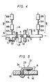
- FIG. 4 An embodiment of the present invention shown in Figure 4 has the same basic structure as the circuit of Figure 1.
- the circuit of Figure 4 differs from that of Figure 1 in that adjustable conductive wire elements are provided to control accurately the impedances provided by the transmission line and open-ended stubs.
- conductive wire elements 21 and 22 are provided for impedance adjustment and are arranged near the signal transmission line 6 and the open-ended stub 11, respectively.
- Both the conductive wire elements 21 and 22 are formed of substantially the same materials and, as is shown more clearly in Figure 5, which is a cross-sectional view taken through a section line A-A' in Figure 4, the wire element 21 comprises an inner, metallic conductive material or wire 23 having a non-conductive cover or sheath 24 arranged around it.
- the insulative cover or sheath 24 can be of polytetrafluoroethylene (for example that sold under the trademark "Teflon”) or similar insulative material having a low high-frequency loss.
- Teflon polytetrafluoroethylene
- One end of the conductive element 21 is bared of its insulative sheath 24 so that the inner wire or conductor 23 is exposed and this exposed end is soldered or otherwise electrically connected to the conductive ground plane 16 arranged on the side of the dielectric substrate 15 opposite the conductive strip pattern or signal transmission line 6.
- the orientation of each of the wire elements 21 and 22 can be adjusted freely, using the soldered end as a supporting point.
- the distances from the wire elements 21 and 22 to the signal transmission line 6 and open-ended stub 11, respectively, can be made smaller or larger by movements as shown by an arrow A in Figure 5, and the angular positions at which the wire elements 21 and 22 intersect the signal transmission line 6 and open-ended stub 11, respectively, can be changed by movements in the directions represented by arrows B and C, respectively, in Figure 4.
- the wire elements 21 and 22 are arranged to be closer to the transmission line 6 and open-ended stub 11, a parallel capacitance is added to the transmission line 6 and open-ended stub 11, so that the effective length of each line can be changed equivalently, thereby carrying out an input impedance adjustment.
- the impedance adjusting measures described above need not be limited to such high frequency use but can be applied to any other use for microstrip circuits.
- Such other uses might comprise, for example, a mixer circuit utilised in a super high frequency to ultra high frequency converter, impedance adjustment at the output side of a local oscillator circuit, or impedance matching adjustment of a circulator.
- the impedance adjusting device need not be employed with each and every open-ended stub in the circuit, but can be employed as necessary to provide appropriate impedance matching adjustment.
- the impedance adjustment can be carried out simply by moving the free end of the conductive wire element, the other end of which is attached to the conductive ground plane of the microstrip circuit, and because such impedance adjusting element is provided in proximity to the signal transmission line or impedance stub, one need only change the spatial positions of the wire element relative to the signal transmission line or the open-ended stub in order to perform impedance adjustment, and bothersome and inefficient steps, such as soldering elements of an adjusting pattern, need not be performed.
- the impedance adjustment technique is specifically suited for low-cost mass production. That is, the impedance adjustment, or adjustment of the input/output voltage standing wave ratio (VSWR) of a high frequency microstrip amplifier, can be performed easily and the burdensome steps necessary in the above-described previous proposal are eliminated.
- VSWR input/output voltage standing wave ratio
Landscapes
- Physics & Mathematics (AREA)
- Electromagnetism (AREA)
- Microwave Amplifiers (AREA)
- Waveguide Connection Structure (AREA)
- Waveguides (AREA)
Claims (2)
- Mikrostreifenschaltung mit:
einer Signalübertragungsleitung (6),
einem mit der Signalübertragungsleitung (6) verbundenen Schaltkreiselement (1),
einem Impedanzanpassungselement in Form einer parallel zur Signalübertragungsleitung (6) geschalteten offenen Stichleitung (11),
einer Erdungsfläche (16),
gekennzeichnet durch
ein elektrisch leitendes Drahtelement (21, 22), welches aus einem elektrisch leitenden Metalldraht (23) gebildet ist, der durch eine isolierende Hülle (24) abgedeckt und in der Nähe der Signalübertragungsleitung (6) oder der offenen Stichleitung (11) angeordnet ist, wobei der Draht (23) des Drahtelements (21, 22) an einem Ende an die Erdungsfläche (16) gelötet ist, wobei das Drahtelement (21, 22) über der Übertragungsleitung oder der Stichleitung frei im Raum bewegbar ist, wobei das eine Ende des Drahtes (23) als ein Stützpunkt wirkt, wobei die räumliche Position des leitenden Drahtelements (21, 22) relativ zur Signalübertragungsleitung (6) oder Stichleitung (11) variiert werden kann, um eine wirksame Impedanz der Signalübertragungsleitung (6) relativ zum Schaltkreiselement (1) zu variieren. - Mikrostreifenschaltung nach Anspruch 1, in welcher ein elektrisch leitendes Drahtelement (21) neben der Signalübertragungsleitung (6) und ein anderes elektrisch leitendes Drahtelement (22) neben der offenen Stichleitung (11) angeordnet ist.
Applications Claiming Priority (2)
| Application Number | Priority Date | Filing Date | Title |
|---|---|---|---|
| JP59035788A JPS60180202A (ja) | 1984-02-27 | 1984-02-27 | ストリツプ線路回路 |
| JP35788/84 | 1984-02-27 |
Publications (3)
| Publication Number | Publication Date |
|---|---|
| EP0154496A2 EP0154496A2 (de) | 1985-09-11 |
| EP0154496A3 EP0154496A3 (en) | 1988-01-27 |
| EP0154496B1 true EP0154496B1 (de) | 1992-05-13 |
Family
ID=12451647
Family Applications (1)
| Application Number | Title | Priority Date | Filing Date |
|---|---|---|---|
| EP85301286A Expired - Lifetime EP0154496B1 (de) | 1984-02-27 | 1985-02-26 | Mikrostreifenschaltungen |
Country Status (7)
| Country | Link |
|---|---|
| US (1) | US4618838A (de) |
| EP (1) | EP0154496B1 (de) |
| JP (1) | JPS60180202A (de) |
| KR (1) | KR920009670B1 (de) |
| AU (1) | AU573692B2 (de) |
| CA (1) | CA1233532A (de) |
| DE (1) | DE3586007D1 (de) |
Families Citing this family (15)
| Publication number | Priority date | Publication date | Assignee | Title |
|---|---|---|---|---|
| JPS63199508A (ja) * | 1987-02-13 | 1988-08-18 | Sharp Corp | 低雑音マイクロ波増幅回路 |
| FI78580C (fi) * | 1987-11-23 | 1989-08-10 | Solitra Oy | Mikrobandkrets och foerfarandet att reglera dess egenskaper. |
| US5065117A (en) * | 1989-06-06 | 1991-11-12 | Sharp Kabushiki Kaisha | Microwave circuit |
| WO1992003887A1 (en) * | 1990-08-23 | 1992-03-05 | Hills Industries Limited | Modular amplifier system for television distribution |
| JP2788838B2 (ja) * | 1993-05-31 | 1998-08-20 | 日本電気株式会社 | 高周波集積回路 |
| FR2765047A1 (fr) * | 1997-06-20 | 1998-12-24 | Trt Lucent Technologies | Dispositif de telebouclage |
| US6392504B1 (en) | 1999-12-08 | 2002-05-21 | Innerwireless, Inc. | Device for coupling radio frequency energy from various transmission lines using variable impedance transmission lines with cable tap |
| JP2001244308A (ja) * | 2000-02-25 | 2001-09-07 | Mitsubishi Electric Corp | 高周波信号用のプローブ |
| US7541889B2 (en) * | 2003-06-26 | 2009-06-02 | Intel Corporation | Pulse coupling apparatus, systems, and methods |
| TWI236234B (en) * | 2004-03-26 | 2005-07-11 | Wistron Neweb Corp | Radiowave receiving device |
| JP4638711B2 (ja) * | 2004-10-27 | 2011-02-23 | 株式会社エヌ・ティ・ティ・ドコモ | 共振器 |
| CN100555744C (zh) * | 2004-11-18 | 2009-10-28 | 富士康(昆山)电脑接插件有限公司 | 天线及其阻抗匹配方法 |
| US7239165B2 (en) * | 2005-03-31 | 2007-07-03 | Intel Corporation | Pulse transport apparatus, systems, and methods |
| CN105301378B (zh) * | 2014-07-08 | 2019-02-01 | 苏州普源精电科技有限公司 | 具有微带线可调电容的射频测量装置及微带线可调电容 |
| CN113109692B (zh) * | 2021-03-31 | 2023-03-24 | 中国电子科技集团公司第十三研究所 | 微带电路调试方法及调节模块 |
Family Cites Families (8)
| Publication number | Priority date | Publication date | Assignee | Title |
|---|---|---|---|---|
| US2410656A (en) * | 1943-06-24 | 1946-11-05 | Rca Corp | Tuned ultra high frequency transformer |
| GB676133A (en) * | 1950-02-09 | 1952-07-23 | British Thomson Houston Co Ltd | Improvements relating to electrically resonant windows |
| US2794174A (en) * | 1952-05-08 | 1957-05-28 | Itt | Microwave transmission systems and impedance matching devices therefor |
| US2735073A (en) * | 1952-08-02 | 1956-02-14 | Bandpass | |
| US2897460A (en) * | 1954-06-25 | 1959-07-28 | Hazeltine Research Inc | Transmission-line impedance-matching apparatus |
| US3796976A (en) * | 1971-07-16 | 1974-03-12 | Westinghouse Electric Corp | Microwave stripling circuits with selectively bondable micro-sized switches for in-situ tuning and impedance matching |
| US3925740A (en) * | 1974-07-19 | 1975-12-09 | Itt | Tuning structures for microstrip transmission lines |
| US4472690A (en) * | 1982-06-14 | 1984-09-18 | Rockwell International Corporation | Universal transistor characteristic matching apparatus |
-
1984
- 1984-02-27 JP JP59035788A patent/JPS60180202A/ja active Pending
-
1985
- 1985-02-12 US US06/700,915 patent/US4618838A/en not_active Expired - Lifetime
- 1985-02-12 CA CA000474070A patent/CA1233532A/en not_active Expired
- 1985-02-13 KR KR1019850000867A patent/KR920009670B1/ko not_active Expired
- 1985-02-14 AU AU38718/85A patent/AU573692B2/en not_active Ceased
- 1985-02-26 EP EP85301286A patent/EP0154496B1/de not_active Expired - Lifetime
- 1985-02-26 DE DE8585301286T patent/DE3586007D1/de not_active Expired - Lifetime
Also Published As
| Publication number | Publication date |
|---|---|
| EP0154496A3 (en) | 1988-01-27 |
| EP0154496A2 (de) | 1985-09-11 |
| KR920009670B1 (ko) | 1992-10-22 |
| KR850006263A (ko) | 1985-10-02 |
| DE3586007D1 (de) | 1992-06-17 |
| US4618838A (en) | 1986-10-21 |
| CA1233532A (en) | 1988-03-01 |
| JPS60180202A (ja) | 1985-09-14 |
| AU3871885A (en) | 1985-09-05 |
| AU573692B2 (en) | 1988-06-16 |
Similar Documents
| Publication | Publication Date | Title |
|---|---|---|
| EP0154496B1 (de) | Mikrostreifenschaltungen | |
| Menzel et al. | A microstrip patch antenna with coplanar feed line | |
| KR100455498B1 (ko) | 프린트안테나 | |
| KR20190051208A (ko) | Dgs를 포함하는 위상 천이기 및 이를 포함하는 전파 통신 모듈 | |
| US5262739A (en) | Waveguide adaptors | |
| US3965445A (en) | Microstrip or stripline coupled-transmission-line impedance transformer | |
| AU634433B2 (en) | Coplanar 3db quadrature coupler | |
| EP0984504A2 (de) | Wandler für elektrisch transversale oder quasi-transversale Moden in Hohlleitermoden | |
| US4749969A (en) | 180° hybrid tee | |
| US3760304A (en) | Slot line | |
| US7283015B1 (en) | Device for impedance matching radio frequency open wire transmission lines | |
| Minnis | Classes of sub-miniature microwave printed circuit filters with arbitrary passband and stopband widths | |
| JPH08279704A (ja) | 終端器用抵抗素子 | |
| US4799032A (en) | Directional coupler | |
| Keller et al. | Active millimetre-wave aperture-coupled microstrip patch antenna array | |
| Joseph et al. | Antenna array and GaAs phase shifter MMIC for millimeter wave beamforming-co-simulation and measurements | |
| US4034321A (en) | Method and apparatus for microstrip termination | |
| CA2228906A1 (en) | Impedance converting device | |
| US20190372232A1 (en) | Tuneable waveguide transition | |
| JPS59117801A (ja) | マイクロストリツプ回路 | |
| EP1820236B1 (de) | Übertragungsanordnung | |
| RU2729513C1 (ru) | Полосковый фазовращатель | |
| GB2192494A (en) | Strip transmission line impedance transformation | |
| US5103196A (en) | Microstrip line having a changed effective line length | |
| KR100367623B1 (ko) | 공기 절연층을 갖는 마이크로스트립 구조의 모놀리식마이크로웨이브 아이.씨.용 3 dB 커플러 및 그 제작 방법 |
Legal Events
| Date | Code | Title | Description |
|---|---|---|---|
| PUAI | Public reference made under article 153(3) epc to a published international application that has entered the european phase |
Free format text: ORIGINAL CODE: 0009012 |
|
| AK | Designated contracting states |
Designated state(s): DE FR GB NL |
|
| PUAL | Search report despatched |
Free format text: ORIGINAL CODE: 0009013 |
|
| AK | Designated contracting states |
Kind code of ref document: A3 Designated state(s): DE FR GB NL |
|
| 17P | Request for examination filed |
Effective date: 19880629 |
|
| 17Q | First examination report despatched |
Effective date: 19891220 |
|
| GRAA | (expected) grant |
Free format text: ORIGINAL CODE: 0009210 |
|
| AK | Designated contracting states |
Kind code of ref document: B1 Designated state(s): DE FR GB NL |
|
| REF | Corresponds to: |
Ref document number: 3586007 Country of ref document: DE Date of ref document: 19920617 |
|
| ET | Fr: translation filed | ||
| PLBE | No opposition filed within time limit |
Free format text: ORIGINAL CODE: 0009261 |
|
| STAA | Information on the status of an ep patent application or granted ep patent |
Free format text: STATUS: NO OPPOSITION FILED WITHIN TIME LIMIT |
|
| 26N | No opposition filed | ||
| PGFP | Annual fee paid to national office [announced via postgrant information from national office to epo] |
Ref country code: GB Payment date: 20010221 Year of fee payment: 17 Ref country code: DE Payment date: 20010221 Year of fee payment: 17 |
|
| REG | Reference to a national code |
Ref country code: GB Ref legal event code: IF02 |
|
| PGFP | Annual fee paid to national office [announced via postgrant information from national office to epo] |
Ref country code: FR Payment date: 20020212 Year of fee payment: 18 |
|
| PG25 | Lapsed in a contracting state [announced via postgrant information from national office to epo] |
Ref country code: GB Free format text: LAPSE BECAUSE OF NON-PAYMENT OF DUE FEES Effective date: 20020226 |
|
| PGFP | Annual fee paid to national office [announced via postgrant information from national office to epo] |
Ref country code: NL Payment date: 20020228 Year of fee payment: 18 |
|
| PG25 | Lapsed in a contracting state [announced via postgrant information from national office to epo] |
Ref country code: DE Free format text: LAPSE BECAUSE OF NON-PAYMENT OF DUE FEES Effective date: 20020903 |
|
| GBPC | Gb: european patent ceased through non-payment of renewal fee |
Effective date: 20020226 |
|
| PG25 | Lapsed in a contracting state [announced via postgrant information from national office to epo] |
Ref country code: NL Free format text: LAPSE BECAUSE OF NON-PAYMENT OF DUE FEES Effective date: 20030901 |
|
| PG25 | Lapsed in a contracting state [announced via postgrant information from national office to epo] |
Ref country code: FR Free format text: LAPSE BECAUSE OF NON-PAYMENT OF DUE FEES Effective date: 20031031 |
|
| NLV4 | Nl: lapsed or anulled due to non-payment of the annual fee |
Effective date: 20030901 |
|
| REG | Reference to a national code |
Ref country code: FR Ref legal event code: ST |