EP0152922A2 - Method and system for processing digital video signal incorporating phase-correction feature - Google Patents
Method and system for processing digital video signal incorporating phase-correction feature Download PDFInfo
- Publication number
- EP0152922A2 EP0152922A2 EP85101634A EP85101634A EP0152922A2 EP 0152922 A2 EP0152922 A2 EP 0152922A2 EP 85101634 A EP85101634 A EP 85101634A EP 85101634 A EP85101634 A EP 85101634A EP 0152922 A2 EP0152922 A2 EP 0152922A2
- Authority
- EP
- European Patent Office
- Prior art keywords
- signal
- phase
- video signal
- reference signal
- set forth
- Prior art date
- Legal status (The legal status is an assumption and is not a legal conclusion. Google has not performed a legal analysis and makes no representation as to the accuracy of the status listed.)
- Granted
Links
Images


Classifications
-
- H—ELECTRICITY
- H04—ELECTRIC COMMUNICATION TECHNIQUE
- H04N—PICTORIAL COMMUNICATION, e.g. TELEVISION
- H04N9/00—Details of colour television systems
- H04N9/79—Processing of colour television signals in connection with recording
- H04N9/87—Regeneration of colour television signals
- H04N9/89—Time-base error compensation
-
- G—PHYSICS
- G11—INFORMATION STORAGE
- G11B—INFORMATION STORAGE BASED ON RELATIVE MOVEMENT BETWEEN RECORD CARRIER AND TRANSDUCER
- G11B20/00—Signal processing not specific to the method of recording or reproducing; Circuits therefor
- G11B20/10—Digital recording or reproducing
- G11B20/10527—Audio or video recording; Data buffering arrangements
Definitions
- the present invention relates generally to a method and a system for processing a video signal. More particularly, the invention relates to a method and system for processing input video signal, which has sampling points of uniform phase so as to be vertically aligned on a screen.
- TBC time base correction circuit
- the time base correction circuit converts the analog input video signal into a pulse train indicative of a fixed number of sampled video signal values between successive pulses of a synchronizing signal contained in the input video signal, and stores the sampled video signal values in a memory. Thereafter, a read-out clock signal is produced in phase with the sampling phase of the analog input video signal. The sampled data is read out from the memory synchronously with this clock signal to re-form the analog video signal.
- This processing by means of the time base correction circuit has been generally accepted as an effective way of removing jitter from the analog input video signal. However, since this process always requires analog-to-digital conversion and digital-to-analog conversion, it inevitably degrades the video signal content. Also, this conventional circuit construction is complicated and bulky due to the presence of the time base correction circuit.
- the phase difference between each line of the input analog signal and a reference phase is detected and used to derive an error signal, and a delayed signal is produced by delaying the video signal by a predetermined period, namely one horizontal scan period.
- the phase of each sampling point of each horizontal line is adjusted in such a manner that phase deviation for the entire line corresponding to the current value of the error signal is distributed uniformly over all of the sampling points in the current horizontal line.
- phase of corresponding sampling points can be vertically aligned without a time base correction circuit.
- a method for processing digital video signal comprises the steps of:
- a system for processing an input video signal includes a detector which detects the phase difference between the input analog signal and a reference phase and produces an error signal indicative thereof, and a delay circuit which produces a delayed signal by delaying the video sigal for a predetermined period.
- the system further includes a phase-correction circuit in which the phase of each sampling point on each horizontal line is corrected by distributing the phase difference corresponding to the value of error signal evenly overall of the sampling points within one horizontal line interval.
- a system for processing an input video signal comprises a first detector measuring the phase of the analog input video signal at a given timing relative to a reference signal phase and deriving the phase difference therebetween, a delay circuit delaying the input video signal for a given period to obtain a delayed video signal, an error detector measuring possible spurious phase error in the input video signal by measuring the rate of change of the phase difference between the input video signal and the reference signal, a clock pulse generator means for producing a predetermined number of clock pulses in each horizontal line interval, the clock pulses being derived from the reference signal by shifting the phase of every pulse of the reference signal by the measured phase difference so as to be in phase with the video input signal and shifting the phase of each pulse of the phase-shifted reference signal to an extent derived by distributing the measured spurious phase error among the predetermined number of clock pulses for each horizontal line, and a sampling signal generator means for deriving the sampling signal from the clock signal.
- the preferred embodiment of a video signal processing system in accordance with the present invention includes a low-pass filter 1 through which an analog input video signal V IN is input to a delay circuit 2 which may comprise a delay line 2B imposing a time delay slightly longer than one horizontal line interval, and which will be referred to hereinafter as ' '1H delay".
- Output S 1 of the 1H delay 2 now retarded by slightly more than one horizontal line scan interval, is conducted to an analog-to-digital (A/D) converter 5 via a low-pass filter 3 and an amplifier 4.
- A/D converter 5 converts the received analog signal a digital video signal V 0 .
- the 1H delay 2 includes an oscillator 2A, which produces an output having a frequency four times that of a color subcarrier frequency f , and a delay line 2B, which will be referred to hereafter as "1H delay line".
- “1H delay line” may be a charge-coupled device (CCD), for example, and is triggered by the output of the oscillator 2A.
- the A/D converter 5 receives a sampling clock signal CK from a sampling clock generator or generating means 10.
- the A/D converter 5 samples the 1H delay output S 1 in response to each sampling clock signal pulse CK. Therefore, the 1H delay output S 1 is sampled at a timing corresponding to the pulse period of the sampling clock signal.
- the analog-to-digital converter 5 converts the sampled analog signal level into a digital value and outputs a digital video signal V 0 in the form of a digital pulse train.
- the sampling clock generator 10 comprises a horizontal synchronizing signal extracting circuit 11 which includes a horizontal synchronizing signal separator circuit 12 and a burst signal gate 13.
- the horizontal synchronizing signal separator circuit 12 receives the analog input video signal V IN and separates a horizontal synchronizing signal H from the input video signal.
- the horizotal synchronizing signal separator circuit 12 derives a gate signal S2 having a gate period corresponding to the period of the burst signal of the input video signal V IN .
- the gate signal S 2 is supplied to the burst gate 13.
- the burst gate 13 responds to the gate signal S 2 by extracting a burst signal BUR from the input video signal V IN and supplying the extracted burst signal BUR to an input phase detector circuit 14.
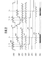
- the waveform of the burst signal BUR is shown in (A) of Fig. 2.
- the horizontal synchronizing signal H separated by the horizontal synchronizing signal separator circuit 12 is supplied to a reference frequency signal generator 15 which comprises a phase-locked loop (PLL).
- the reference frequency signal generator 15 is responsive to the horizontal synchronizing signal H to produce a reference frequency signal SC having a frequency to that of the color subcarrier frequency f sc .
- the reference frequency signal SC is input to the input phase detector 15.
- the waveform of the reference frequency signal SC is seen in (C) of Fig. 2.
- the input phase detector 14 has a phase difference detector 21.
- the phase difference detector is 21 is triggered by a positive-going zero crossing of the burst signal BUR from the burst gate 13, as shown at time t i of Fig.2.
- the phase difference detector 15 measures the phase difference A6 between the phase of the reference frequency signal SC of (C) of Fig. 2 and the burst signal BUR of (A) of Fig. 2.
- the phase difference detector 21 then produces a phase difference indicative signal S 3 according to the measured phase difference A6.
- the phase difference indicative signal S 3 is then output to a phase-shifting circuit 22 in the input phase detector 15 at the next positive-going zero point of the burst signal BUR as shown at time t 2 of Fig. 2.
- the phase-shifting circuit 22 adjusts the phase of the reference frequency signal SC to an extent corresponding to the value of the phase difference indicative signal S 3 which represents the phase difference ⁇ between the burst signal BUR (Fig. 2A) and the reference frequency signal (Fig. 2C).
- the phase-shifting circuit 22 outputs a signal S 4 with the same frequency as the reference frequency signal but phase-shifted to an extent corresponding to the phase difference indicative signal value ( ⁇ ), which signal S 4 will be referred to hereafter as "phase-shifted reference frequency signal' '.
- phase-shifted reference frequency signal S 4 is thus in phase with the burst signal BUR.
- the phase-shifted reference frequency signal S 4 is applied to a velocity-error detector 23.
- the velocity-error detector 23 checks the phase difference between the burst signal BUR and the phase-shifed reference signal S 4 , which should match the phase deviation measured by the phase-shifting circuit 22 when the rotary video head is turning at precisely its rated drive speed.
- the velocity-error detector 23 outputs an error-indicative signal 8 5 in the form of a direct-current voltage representative of the derived phase difference at time t 2 .
- the error signal S 5 is transmitted to a sample/hold circuit 26.
- the input phase detector 14 in order to detect phase of the analog input video signal VIN, the input phase detector 14 produces a phase-shifted reference frequency signal S 4 the frequency of the reference frequency signal of the reference frequency signal generator 15 and the phase of the burst signal BUR, and also produces an error signal s 5 indicative of subsequently occurring phase deviation between the burst signal BUR and the phase-shifted reference frequency signal S 4 .
- Close inspection of analog input video signals reveals that the phases of the horizontal synchronizing signal H and the burst signal BUR most often differ. Therefore, one of the phase of the horizontal synchronizing signal H or the phase of the burst signal BUR must be taken as the phase of the input video signal.
- the horizontal synchronizing signal H is a rectangular waveform signal and therefore includes a plurality of frequency components.
- the burst signal BUR is an analog frequency signal. Therefore, it is easier to detect the signal phase of the burst signal BUR than that of the horizontal synchronizing signal H. This allows more accurate detection of the phase of the input video signal. For this reason, in the shown embodiment, the phase of the burst signal is preferred for use in determining the phase of the input video signal.
- a phase correction circuit 25 includes the sample/hold circuit 26 which is connected for input from the velocity-error detector 23 as set forth above.
- the sample/hold circuit 26 latches the value of the error signal S 5 at time t 3 determined on the basis of a delayed burst signal BUD extracted from 1H delay output S 1 .
- the 1H delay output S 1 of the 1H delay 2 is applied to a delayed burst gate 33 in a delayed signal extracting circuit 32, via an amplifier 31, as delayed input S 6'
- the waveform of the delayed input S 6 is illustrated in (B) of Fig. 2.
- the time delay imposed by the 1H delay 2 can best be understood by noting that the time points t 2 of (A) and t 13 of (B) correspond to the same screen pixel.
- the delayed output S 1 is retarded by a full scan line period plus the short interval tg-t 2 or t 13 -t 12 to allow for signal processing delays.
- the delayed burst signal BUD is derived from the preceding horizontal line while the error signal S 5 is derived from the current burst signal BUR.
- the delayed signal extracting circuit 32 also has a gate signal generator 34.
- the gate signal generator 34 which may, for example, comprise a monostable multivibrator, produces an extracting gate signal S 7 as described in detail later.
- the delayed burst gate 33 responds to the extracting gate signal S 7 by extracting the burst signal component BUD from the delayed input S 6 from the amplifier 31.
- the burst signal BUD thus extracted by the delayed burst gate 33 is supplied to the sample/hold circuit 26.
- the extracting gate signal generator 34 is connected for input from the horizontal synchronizing signal separator circuit 12 in order to receive the horizontal synchronizing signal H.
- the extracting gate signal generator 34 is responsive to the leading edge of the horizontal synchronizing signal H to output the extracting gate signal S 7 having a period corresponding to the period over which the burst signal BUR appears in the input video signal. Since, the delayed input S 6 from the amplifier 31 is delayed by slightly more than one horizontal line interval, the timing of the horizontal synchronizing signal H in the 1H delay output S 1 is somewhat offset from that of the input video signal. Therefore, the extracting gate signal generator 34 delays by this known offset the horizontal synchronizing signal H extracted from the input video signal V IN to ensure that all of the delayed burst signal BUD can be extracted from the delayed input S 6 .
- the delayed burst signal BUD from the delayed burst gate 33 is also input to a phase difference detector 36 which is also connected to the reference frequency signal generator 15 to receive the reference frequency signal SC.
- the phase difference detector 36 compares the signal phases of the delayed burst signal BUD from the delayed burst gate 32 and the reference frequency signal SC from the reference frequency signal generator 15 to derive the phase difference therebetween.
- the phase difference detector 36 produces a phase-shifting control signal S 9 having a value indicative of the phase difference between the delayed burst signal BUD-and the reference frequency signal.
- the phase difference detector 36 operates slightly differently than the phase difference detector 21 described above. At the second positive-going zero-crossing point of the delayed burst signal BUD, the phase difference detector 36 compares the phases of the delayed burst signal BUD and the reference frequency signal SC. The phase-shifting control signal S 9 . which corresponds the phase difference indicative signal S 3 of the phase difference detector 21, is then output immediately to a phase-shifting circuit 37.
- the phase shifting circuit 37 receives the phase-shifting control signal s 9 from the phase difference detector 36 and shifts the phase of the reference frequency signal SC to an extent corresponding to the value of the phase-shifting control signal S 9 from the phase difference detector 36.
- the phase-shifting circuit 37 outputs a phase-shifted frequency signal S 10 which is in phase with the delayed burst signal BUR.
- the phase-shifted frequency signal S 10 from the phase-shifting circuit 37 is supplied to a phase modulation circuit 38.
- the phase modulation circuit 38 also receives the output S 11 of the sample/hold circuit 26.
- the phase modulation circuit 38 adjusts the phase of the phase-shifted frequency signal S 10 from the phase-shifting circuit 37 to an extent determined by the output S 11 of the sample/hold circuit 26, which is indicative of the phase difference between the burst signal BUR and the phase-shifted reference signal S 4 .
- the adjustment of the signal phase of the phase-shifted frequency signal S 10 is performed gradually and proportionally over a period corresponding to one horizontal line interval.
- the phase modulation circuit 38 outputs the resulting frequency signal phase-adjusted as described above, for use as a clock signal S12.
- the waveform of the clock S12 from the phase modulation circuit 38 is shown in (G) of Fig. 2. Although not noticeable in Fig. 2(G), the phase of each successive pulse of the clock S12 varies slightly, as will become clear later.
- Fig. 3 shows the detailed structure of the phase modulation circuit 38.
- the phase modulation circuit 38 includes a level comparator 51.
- a reference signal S 21 is applied to the inverting input (-) of the level comparator 51.
- the reference signal is a ramp signal having a waveform as shown in Fig. 4.
- the reference signal S 21 starts at a value V S11 corresponding to the level of the output S 11 of the sample/hold circuit 26, at time t 3 and then drops linearly to zero over a period equal to one horizontal scan line interval (1H), as shown in Fig. 4.
- the phase modulation circuit 38 also has a sawtooth signal generator 52 which receives the phase-shifted frequency signal S 10 from the phase-shifting circuit 37, the waveform of which is illustrated in (A) of Fig. 5.
- the sawtooth signal generator 52 outputs a sawtooth signal S 22 with the same period T R as the phase-shifted frequency signal S 10 .
- the waveform of the sawtooth signal S22 has been illustrated in (B) of Fig. 5.
- the sawtooth signal S 22 is input to the non-inverting input (+) of the level comparator 51.
- the level comparator 51 outputs a comparator signal S23 which remains HIGH for the period during which the signal level of the sawtooth signal S 22 exceeds the reference signal level S Z1 .
- a typical waveform of the comparator output S23 is illustrated in ( C ) of Fig. 5.
- the comparator signal S 23 is fed to a waveform shaping circuit 53.
- When triggered by the leading edge of the comparator signal S 23 to the waveform shaping circuit 53 produce a pulse with a predetermined pulse width.
- the output train of these pulses forms clock signal S12 of (D) of Fig. 5.
- the period T R ' of the clock S 12 may differ slightly from that of the reference frequency signal SC of the reference frequency signal generator 15, the difference being dependent on the value of signal S 11 and on the position of each pulse in the horizontal scan line.
- the pulses falling at the center of each horizontal line will always be in precise alignment vertically, and due to the linear nature of the sawtooth signal S 22 and the reference signal S 21 , the phase error will be divided symmetrically to either side of the screen. This maximizes image quality by limitting the maximum vertical offset and by providing the best accuracy in the center of the image.
- the phase at which the sawtooth signal level first exceeds the reference level defined by the reference signal S21 advances as the reference level of the reference signal S 21 drops. Therefore, the period T R ' of the clock S 12 varies gradually and continuously at a rate depending upon the rate of decrease of the reference signal determined by the value of the signal S 11 .
- phase modulation technique set forth above covers an entire cycle of the ramp signal S 21 , i.e. one horizontal line interval, over which the value V S11 represented by the output S11 of the sample/hold circuit 26 is uniformly distributed, the phase error for each horizontal scan line is divided equally among all of the pulses of the clock S12 for that scan line.
- each scan line will have the same number of pixels or color clock pulses S 12 , and the horizontal offset between pixels of adjoining scan lines will be reduced to a negligible level.
- the clock S 12 thus produced by the phase modulation circuit 38 is supplied to a multiplier 42 through a temperature compensation circuit 41.
- the multiplier 42 multiplies the clock frequency by 4 to generate a frequency 4f sc four-times higher than the frequency of the reference frequency signal.
- the output of the multiplier 42 serves as sampling clock CK for the A/D converter 5.
- the waveform of the sampling clock CK is shown in (H) of Fig. 2.
- the temperature compensation circuit 41 compensates for phase variation of the sampling clock CK due to temperature variations.
- the temperature compensation circuit 41 has a divider 43 which divides the frequency of the sampling clock CK by four to match the frequency of the clock S 12 of the phase modulation circuit 38.
- the divided output of the divider 43 is fed to a phase difference detector 44 which also receives the clock S 12 from the phase modulation circuit 38.
- the phase difference detector 44 compares the phases of the clock S 12 and the divided output from the divider 43 and outputs a phase difference indicative signal S 25 to a phase-shifting circuit 45 interposed between the phase modulation circuit 38 and the multiplier 42.
- the phase difference indicative signal S 25 has a value representative of the phase difference between the divided output from the divider 43 and the clock S 12 . Therefore, by shifting the phase of the clock S 12 to an extent-equal to the phase difference between the divided output and the clock S12, the phase of the clock S 12 is compensated for possible temperature-dependent variations thereof.
- the phase of the analog input video signal V IN i.e., the phase of the burst signal BUR extracted by the burst gate 13 in response to the gate signal S 2 from the horizontal synchronizing signal separator circuit 12, is compared with the reference frequency signal SC of the reference frequency signal generator 15, which has the same frequency as the color subcarrier frequency f sc , by the phase difference detector 21 of the input phase detector 14.
- the phase difference indicative signal S 3 output by the phase difference detector 21 has a value corresponding to the phase difference between the input video signal phase and the reference frequency signal phase.
- Phase-shifting operation of the phase-shifting circuit 22 in the input phase detector 14 is mediated by the phase difference indicative signal S 3 .
- the phase-shifting circuit 22 shifts the signal phase of the reference frequency signal SC to the extent indicated by the phase difference indicative signal S 3 and outputs the phase-shifted reference frequency signal S 4 , as shown in (D) of Fig. 2, which should be in phase with the burst signal BUR of (A) of Fig. 2.
- the phase-shifted reference frequency signal S 4 is applied to the velocity-error detector 23 at the time t 2 .
- the velocity-error detector 23 measures any existing phase difference between the phase-shifted reference frequency signal 8 4 and the burst signal BUR and produces an error indicative signal S 5 having a value indicative of the derived phase difference.
- the velocity-error detector 23 outputs the error indicative signal S 5 to the sample/hold circuit 26.
- the phase of the delayed burst signal BUD which is extracted from the 1H delayed output S 1 , is compared with the reference frequency signal SC to derive the phase difference therebetween.
- the phase of the reference frequency signal is shifted by the phase-shifting circuit 37 to an extent equal to the phase difference between the delayed burst signal BUD and the reference frequency signal SC in order to match phase with the delayed burst signal.
- the phase-shifted frequency signal S 10 is applied to the phase modulation circuit 38.
- the output S 11 representing the value held in the sample/hold circuit 26 is also applied to the phase modulation circuit 38.
- the phase modulation circuit 38 distributes the phase error indicated by the output S11 from the sample/hold circuit 26 among the pulses of the clock S 12 within one horizontal line interval. Therefore, irrespective of the magnitude of the holding output S 11 , a predetermined number of pulses of clock S 12 can be output in each horizontal line interval.
- the clock S 12 is increased in frequency by four times by the multiplier 42 and output as sampling clock CK.
- the sampling clock CK is output to the A/D converter. Since the clock S 12 of the phase modulation circuit 38 always has a constant, predetermined number of pulses within each horizontal line interval, the sampling clock CK will also always have a constant, predetermined number of pulses.
- the A/D converter 5 is triggered by each pulse of the sampling clock CK to sample the 1H delay output S 1 and output the sampled value as digital video signal V o .
- the 1H delay output S 1 will be sampled at a predetermined constant number of sample points during each horizontal scan line.
- conversion of the analog input video signal V IN into digital video signal V 0 is performed at a constant number of sample point. within each horizontal line interval, even when the analog input video signal is subject to significant jitter.
- the phase offset between corresponding sampling points of each horizontal line is minimized, so that the vertical positions on a screen of corresponding sample points will remain in close alignment.
- phase modulation circuit in the preferred embodiment distributes the phase error linearly among the pulses of the clock signal
- distribution rate of the phase error need not be linear. It is essential only that the distribution be consistent for each horizontal line. Therefore, as long as the phase error is distributed consistently for each horizontal line .and as long as the phases of corresponding sample points can be uniform, any distribution technique may be used to embody the present invention.
- the shown embodiment has been disclosed in terms of analog input video signal processing, in which the clock signal is generated with reference to the 1H delay output produced by delaying the input video signal for one horizontal line interval, it should not be considered essential to have a 1H delay: the delay can be of any convenient length.
Abstract
Description
- The present invention relates generally to a method and a system for processing a video signal. More particularly, the invention relates to a method and system for processing input video signal, which has sampling points of uniform phase so as to be vertically aligned on a screen.
- When an analog input video signal is processed for conversion into a digital video signal in preparation for recording, reproduction, broadcase and so forth, it is be considered good practice to use synchronization and sample gating signals to ensure that the sampling phases of the analog input video signal are aligned in predetermined relationships. For example, when interlacing screen lines by averaging the digital video signal values for screen pixels immediately above and below each interlaced pixel, it is essential that the sampling phases for every line on the screen be aligned to ensure accurate average values. In addition, when using elements such as a noise reducer. a comb filter or the like, the sampling phases, i.e. the position of sampled data in each line of the screen must be vertically aligned.
- Conventionally, a time base correction circuit (TBC) has been employed to match the sampling phases during conversion of an analog video signal into a digital video signal and correct for jitter in the analog input video signal. Digital data sampling is performed on the output of the time base correction circuit.
- In this case, the time base correction circuit converts the analog input video signal into a pulse train indicative of a fixed number of sampled video signal values between successive pulses of a synchronizing signal contained in the input video signal, and stores the sampled video signal values in a memory. Thereafter, a read-out clock signal is produced in phase with the sampling phase of the analog input video signal. The sampled data is read out from the memory synchronously with this clock signal to re-form the analog video signal. This processing by means of the time base correction circuit has been generally accepted as an effective way of removing jitter from the analog input video signal. However, since this process always requires analog-to-digital conversion and digital-to-analog conversion, it inevitably degrades the video signal content. Also, this conventional circuit construction is complicated and bulky due to the presence of the time base correction circuit.
- Therefore, it is an object of the invention to provide a method and system for processing analog input video signal to convert into digital video signal which can align sampling phases without a time base correction circuit and which therefore exhibits a relatively simple circuit layout.
- In order to accomplish the aforementioned and other objects, in a method for processing an input video signal according to the present invention, the phase difference between each line of the input analog signal and a reference phase is detected and used to derive an error signal, and a delayed signal is produced by delaying the video signal by a predetermined period, namely one horizontal scan period. The phase of each sampling point of each horizontal line is adjusted in such a manner that phase deviation for the entire line corresponding to the current value of the error signal is distributed uniformly over all of the sampling points in the current horizontal line.
- By dividing the phase deviation among all of a constant number of sampling points in each horizontal line, the phase of corresponding sampling points can be vertically aligned without a time base correction circuit.
- In accordance with one aspect of the invention, a method for processing digital video signal comprises the steps of:
- measuring the phase of the analog input video signal at a given timing relative to a reference signal phase and deriving the phase difference therebetween;
- delaying the input video signal for a given period to obtain a delayed video signal;
- measuring possible spurious phase error in the input video signal by measuring the rate of change of the phase difference between the input video signal and the reference signal;
- producing a predetermined number of clock pulses in each horizontal line interval, the clock pulses being derived from the reference signal by shifting the phase of every pulse of the reference signal by the measured phase difference so as to be in phase with the video input signal and.shifting the phase of each pulse of the phase-shifted reference signal to an extent derived by distributing the measured spurious phase error among the predetermined number of clock pulses for each horizontal line; and
- deriving the sampling signal from the clock signal.
- On the other hand, in order to accomplish the aforementioned and other objects, a system for processing an input video signal, according to the present invention, includes a detector which detects the phase difference between the input analog signal and a reference phase and produces an error signal indicative thereof, and a delay circuit which produces a delayed signal by delaying the video sigal for a predetermined period. The system further includes a phase-correction circuit in which the phase of each sampling point on each horizontal line is corrected by distributing the phase difference corresponding to the value of error signal evenly overall of the sampling points within one horizontal line interval.
- According to one aspect of the invention, a system for processing an input video signal comprises a first detector measuring the phase of the analog input video signal at a given timing relative to a reference signal phase and deriving the phase difference therebetween, a delay circuit delaying the input video signal for a given period to obtain a delayed video signal, an error detector measuring possible spurious phase error in the input video signal by measuring the rate of change of the phase difference between the input video signal and the reference signal, a clock pulse generator means for producing a predetermined number of clock pulses in each horizontal line interval, the clock pulses being derived from the reference signal by shifting the phase of every pulse of the reference signal by the measured phase difference so as to be in phase with the video input signal and shifting the phase of each pulse of the phase-shifted reference signal to an extent derived by distributing the measured spurious phase error among the predetermined number of clock pulses for each horizontal line, and a sampling signal generator means for deriving the sampling signal from the clock signal.
- The present invention will be understood more fully from the detailed description given herebelow and from the accompanying drawings of the preferred embodiment of the invention, which, however, should not be taken to' limit the invention to the specific embodiment but are for explanation and understanding only.
- In the drawings:
- Fih. 1 is a block diagram of the preferred embodiment of an input video signal processing system according to the present invention;
- Fig. 2 is a timing chart of signals produced by the components in the system of Fig. 1;
- Fig. 3 is a block diagram of a phase modulation circuit of the preferred embodiment shown in Fig. 1;
- Fig. 4 shows the waveform of the reference signal applied to the comparator in the phase modulation circuit in Fig. 3; and
- Fig. 5 is a timing chart illustrating one way of modulating the phase of the read-out clock signal.
- Referring now to the drawings, particularly to Fig. 1, the preferred embodiment of a video signal processing system in accordance with the present invention, includes a low-
pass filter 1 through which an analog input video signal VIN is input to adelay circuit 2 which may comprise adelay line 2B imposing a time delay slightly longer than one horizontal line interval, and which will be referred to hereinafter as ' '1H delay". Output S1 of the1H delay 2, now retarded by slightly more than one horizontal line scan interval, is conducted to an analog-to-digital (A/D)converter 5 via a low-pass filter 3 and anamplifier 4. The output of the1H delay 2 will be referred to hereafter as ' '1H delay output". The A/D converter 5 converts the received analog signal a digital video signal V0. - The
1H delay 2 includes an oscillator 2A, which produces an output having a frequency four times that of a color subcarrier frequency f , and adelay line 2B, which will be referred to hereafter as "1H delay line". "1H delay line" may be a charge-coupled device (CCD), for example, and is triggered by the output of the oscillator 2A. - The A/
D converter 5 receives a sampling clock signal CK from a sampling clock generator or generating means 10. The A/D converter 5 samples the 1H delay output S1 in response to each sampling clock signal pulse CK. Therefore, the 1H delay output S1 is sampled at a timing corresponding to the pulse period of the sampling clock signal. The analog-to-digital converter 5 converts the sampled analog signal level into a digital value and outputs a digital video signal V0 in the form of a digital pulse train. - The
sampling clock generator 10 comprises a horizontal synchronizingsignal extracting circuit 11 which includes a horizontal synchronizingsignal separator circuit 12 and aburst signal gate 13. The horizontal synchronizingsignal separator circuit 12 receives the analog input video signal VIN and separates a horizontal synchronizing signal H from the input video signal. On the basis of the separated horizontal synchronizing signal H, the horizotal synchronizingsignal separator circuit 12 derives a gate signal S2 having a gate period corresponding to the period of the burst signal of the input video signal VIN. The gate signal S2 is supplied to theburst gate 13. Theburst gate 13 responds to the gate signal S2 by extracting a burst signal BUR from the input video signal VIN and supplying the extracted burst signal BUR to an inputphase detector circuit 14. The waveform of the burst signal BUR is shown in (A) of Fig. 2. - On the other hand, the horizontal synchronizing signal H separated by the horizontal synchronizing
signal separator circuit 12 is supplied to a referencefrequency signal generator 15 which comprises a phase-locked loop (PLL). The referencefrequency signal generator 15 is responsive to the horizontal synchronizing signal H to produce a reference frequency signal SC having a frequency to that of the color subcarrier frequency fsc. The reference frequency signal SC is input to theinput phase detector 15. The waveform of the reference frequency signal SC is seen in (C) of Fig. 2. - The
input phase detector 14 has aphase difference detector 21. The phase difference detector is 21 is triggered by a positive-going zero crossing of the burst signal BUR from theburst gate 13, as shown at time ti of Fig.2. When triggered, thephase difference detector 15 measures the phase difference A6 between the phase of the reference frequency signal SC of (C) of Fig. 2 and the burst signal BUR of (A) of Fig. 2. Thephase difference detector 21 then produces a phase difference indicative signal S3 according to the measured phase difference A6. The phase difference indicative signal S3 is then output to a phase-shiftingcircuit 22 in theinput phase detector 15 at the next positive-going zero point of the burst signal BUR as shown at time t2 of Fig. 2. The phase-shifting circuit 22 adjusts the phase of the reference frequency signal SC to an extent corresponding to the value of the phase difference indicative signal S3 which represents the phase difference ΔØ between the burst signal BUR (Fig. 2A) and the reference frequency signal (Fig. 2C). The phase-shiftingcircuit 22 outputs a signal S4 with the same frequency as the reference frequency signal but phase-shifted to an extent corresponding to the phase difference indicative signal value (Δø), which signal S4 will be referred to hereafter as "phase-shifted reference frequency signal' '. As will be apparent from the above and from Fig. 2, the phase-shifted reference frequency signal S4 is thus in phase with the burst signal BUR. The phase-shifted reference frequency signal S4 is applied to a velocity-error detector 23. The velocity-error detector 23 checks the phase difference between the burst signal BUR and the phase-shifed reference signal S4, which should match the phase deviation measured by the phase-shiftingcircuit 22 when the rotary video head is turning at precisely its rated drive speed. The velocity-error detector 23 outputs an error-indicative signal 85 in the form of a direct-current voltage representative of the derived phase difference at time t2. The error signal S5 is transmitted to a sample/hold circuit 26. - As set forth above, in order to detect phase of the analog input video signal VIN, the
input phase detector 14 produces a phase-shifted reference frequency signal S4 the frequency of the reference frequency signal of the referencefrequency signal generator 15 and the phase of the burst signal BUR, and also produces an error signal s5 indicative of subsequently occurring phase deviation between the burst signal BUR and the phase-shifted reference frequency signal S4. Close inspection of analog input video signals reveals that the phases of the horizontal synchronizing signal H and the burst signal BUR most often differ. Therefore, one of the phase of the horizontal synchronizing signal H or the phase of the burst signal BUR must be taken as the phase of the input video signal. The horizontal synchronizing signal H is a rectangular waveform signal and therefore includes a plurality of frequency components. On the other hand, the burst signal BUR is an analog frequency signal. Therefore, it is easier to detect the signal phase of the burst signal BUR than that of the horizontal synchronizing signal H. This allows more accurate detection of the phase of the input video signal. For this reason, in the shown embodiment, the phase of the burst signal is preferred for use in determining the phase of the input video signal. - A
phase correction circuit 25 includes the sample/hold circuit 26 which is connected for input from the velocity-error detector 23 as set forth above. The sample/hold circuit 26 latches the value of the error signal S5 at time t3 determined on the basis of a delayed burst signal BUD extracted from 1H delay output S1. Specifically, the 1H delay output S1 of the1H delay 2 is applied to a delayedburst gate 33 in a delayedsignal extracting circuit 32, via anamplifier 31, as delayed input S6' The waveform of the delayed input S6 is illustrated in (B) of Fig. 2. The time delay imposed by the1H delay 2 can best be understood by noting that the time points t2 of (A) and t13 of (B) correspond to the same screen pixel. Thus the delayed output S1 is retarded by a full scan line period plus the short interval tg-t2 or t13-t12 to allow for signal processing delays. This means that in Fig. 2 the delayed burst signal BUD is derived from the preceding horizontal line while the error signal S5 is derived from the current burst signal BUR. - The delayed
signal extracting circuit 32 also has agate signal generator 34. Thegate signal generator 34, which may, for example, comprise a monostable multivibrator, produces an extracting gate signal S7 as described in detail later. The delayed burstgate 33 responds to the extracting gate signal S7 by extracting the burst signal component BUD from the delayed input S6 from theamplifier 31. The burst signal BUD thus extracted by the delayed burstgate 33 is supplied to the sample/hold circuit 26. - As will be appreciated from Fig. 1, the extracting
gate signal generator 34 is connected for input from the horizontal synchronizingsignal separator circuit 12 in order to receive the horizontal synchronizing signal H. The extractinggate signal generator 34 is responsive to the leading edge of the horizontal synchronizing signal H to output the extracting gate signal S7 having a period corresponding to the period over which the burst signal BUR appears in the input video signal. Since, the delayed input S6 from theamplifier 31 is delayed by slightly more than one horizontal line interval, the timing of the horizontal synchronizing signal H in the 1H delay output S1 is somewhat offset from that of the input video signal. Therefore, the extractinggate signal generator 34 delays by this known offset the horizontal synchronizing signal H extracted from the input video signal VIN to ensure that all of the delayed burst signal BUD can be extracted from the delayed input S6. - The delayed burst signal BUD from the delayed burst
gate 33 is also input to aphase difference detector 36 which is also connected to the referencefrequency signal generator 15 to receive the reference frequency signal SC. Thephase difference detector 36 compares the signal phases of the delayed burst signal BUD from the delayed burstgate 32 and the reference frequency signal SC from the referencefrequency signal generator 15 to derive the phase difference therebetween. Thephase difference detector 36 produces a phase-shifting control signal S9 having a value indicative of the phase difference between the delayed burst signal BUD-and the reference frequency signal. - The
phase difference detector 36 operates slightly differently than thephase difference detector 21 described above. At the second positive-going zero-crossing point of the delayed burst signal BUD, thephase difference detector 36 compares the phases of the delayed burst signal BUD and the reference frequency signal SC. The phase-shifting control signal S9. which corresponds the phase difference indicative signal S3 of thephase difference detector 21, is then output immediately to a phase-shiftingcircuit 37. - The
phase shifting circuit 37 receives the phase-shifting control signal s9 from thephase difference detector 36 and shifts the phase of the reference frequency signal SC to an extent corresponding to the value of the phase-shifting control signal S9 from thephase difference detector 36. The phase-shiftingcircuit 37 outputs a phase-shifted frequency signal S10 which is in phase with the delayed burst signal BUR. The phase-shifted frequency signal S10 from the phase-shiftingcircuit 37 is supplied to aphase modulation circuit 38. Thephase modulation circuit 38 also receives the output S11 of the sample/hold circuit 26. - The
phase modulation circuit 38 adjusts the phase of the phase-shifted frequency signal S10 from the phase-shiftingcircuit 37 to an extent determined by the output S11 of the sample/hold circuit 26, which is indicative of the phase difference between the burst signal BUR and the phase-shifted reference signal S4. The adjustment of the signal phase of the phase-shifted frequency signal S10 is performed gradually and proportionally over a period corresponding to one horizontal line interval. Thephase modulation circuit 38 outputs the resulting frequency signal phase-adjusted as described above, for use as a clock signal S12. The waveform of the clock S12 from thephase modulation circuit 38 is shown in (G) of Fig. 2. Although not noticeable in Fig. 2(G), the phase of each successive pulse of the clock S12 varies slightly, as will become clear later. - Fig. 3 shows the detailed structure of the
phase modulation circuit 38. Thephase modulation circuit 38 includes alevel comparator 51. A reference signal S21 is applied to the inverting input (-) of thelevel comparator 51. The reference signal is a ramp signal having a waveform as shown in Fig. 4. The reference signal S21 starts at a value VS11 corresponding to the level of the output S11 of the sample/hold circuit 26, at time t3 and then drops linearly to zero over a period equal to one horizontal scan line interval (1H), as shown in Fig. 4. - The
phase modulation circuit 38 also has asawtooth signal generator 52 which receives the phase-shifted frequency signal S10 from the phase-shiftingcircuit 37, the waveform of which is illustrated in (A) of Fig. 5. Thesawtooth signal generator 52 outputs a sawtooth signal S22 with the same period TR as the phase-shifted frequency signal S10. The waveform of the sawtooth signal S22 has been illustrated in (B) of Fig. 5. The sawtooth signal S22 is input to the non-inverting input (+) of thelevel comparator 51. Thelevel comparator 51 outputs a comparator signal S23 which remains HIGH for the period during which the signal level of the sawtooth signal S22 exceeds the reference signal level SZ1. A typical waveform of the comparator output S23 is illustrated in (C) of Fig. 5. The comparator signal S23 is fed to awaveform shaping circuit 53. When triggered by the leading edge of the comparator signal S23 to thewaveform shaping circuit 53 produce a pulse with a predetermined pulse width. The output train of these pulses forms clock signal S12 of (D) of Fig. 5. - It should be appreciated that the period TR' of the clock S12 may differ slightly from that of the reference frequency signal SC of the reference
frequency signal generator 15, the difference being dependent on the value of signal S11 and on the position of each pulse in the horizontal scan line. In the shown embodiment, the pulses falling at the center of each horizontal line will always be in precise alignment vertically, and due to the linear nature of the sawtooth signal S22 and the reference signal S21, the phase error will be divided symmetrically to either side of the screen. This maximizes image quality by limitting the maximum vertical offset and by providing the best accuracy in the center of the image. - In the circuit structure of Fig. 3, the phase at which the sawtooth signal level first exceeds the reference level defined by the reference signal S21 advances as the reference level of the reference signal S21 drops. Therefore, the period TR' of the clock S12 varies gradually and continuously at a rate depending upon the rate of decrease of the reference signal determined by the value of the signal S11.
- As will be appreciated herefrom, since the phase modulation technique set forth above covers an entire cycle of the ramp signal S21, i.e. one horizontal line interval, over which the value VS11 represented by the output S11 of the sample/
hold circuit 26 is uniformly distributed, the phase error for each horizontal scan line is divided equally among all of the pulses of the clock S12 for that scan line. Thus, no matter how great the phase error, each scan line will have the same number of pixels or color clock pulses S12, and the horizontal offset between pixels of adjoining scan lines will be reduced to a negligible level. - Returning to Fig. 1, the clock S12 thus produced by the
phase modulation circuit 38 is supplied to amultiplier 42 through a temperature compensation circuit 41. According to the shown embodiment, themultiplier 42 multiplies the clock frequency by 4 to generate a frequency 4f sc four-times higher than the frequency of the reference frequency signal. The output of themultiplier 42 serves as sampling clock CK for the A/D converter 5. The waveform of the sampling clock CK is shown in (H) of Fig. 2. - The temperature compensation circuit 41 compensates for phase variation of the sampling clock CK due to temperature variations. The temperature compensation circuit 41 has a
divider 43 which divides the frequency of the sampling clock CK by four to match the frequency of the clock S12 of thephase modulation circuit 38. The divided output of thedivider 43 is fed to aphase difference detector 44 which also receives the clock S12 from thephase modulation circuit 38. Thephase difference detector 44 compares the phases of the clock S12 and the divided output from thedivider 43 and outputs a phase difference indicative signal S25 to a phase-shiftingcircuit 45 interposed between thephase modulation circuit 38 and themultiplier 42. The phase difference indicative signal S25 has a value representative of the phase difference between the divided output from thedivider 43 and the clock S12. Therefore, by shifting the phase of the clock S12 to an extent-equal to the phase difference between the divided output and the clock S12, the phase of the clock S12 is compensated for possible temperature-dependent variations thereof. - The operation of the preferred embodiment of input video processing system according to the present invention will be described with reference mainly to Figs. 1 and 2. At the time t1 in Fig. 2, the phase of the analog input video signal VIN, i.e., the phase of the burst signal BUR extracted by the
burst gate 13 in response to the gate signal S2 from the horizontal synchronizingsignal separator circuit 12, is compared with the reference frequency signal SC of the referencefrequency signal generator 15, which has the same frequency as the color subcarrier frequency fsc, by thephase difference detector 21 of theinput phase detector 14. The phase difference indicative signal S3 output by thephase difference detector 21 has a value corresponding to the phase difference between the input video signal phase and the reference frequency signal phase. Phase-shifting operation of the phase-shiftingcircuit 22 in theinput phase detector 14 is mediated by the phase difference indicative signal S3. The phase-shiftingcircuit 22 shifts the signal phase of the reference frequency signal SC to the extent indicated by the phase difference indicative signal S3 and outputs the phase-shifted reference frequency signal S4, as shown in (D) of Fig. 2, which should be in phase with the burst signal BUR of (A) of Fig. 2. The phase-shifted reference frequency signal S4 is applied to the velocity-error detector 23 at the time t2. - The velocity-
error detector 23 measures any existing phase difference between the phase-shifted reference frequency signal 84 and the burst signal BUR and produces an error indicative signal S5 having a value indicative of the derived phase difference. The velocity-error detector 23 outputs the error indicative signal S5 to the sample/hold circuit 26. - At the time t3, the phase of the delayed burst signal BUD, which is extracted from the 1H delayed output S1, is compared with the reference frequency signal SC to derive the phase difference therebetween. The phase of the reference frequency signal is shifted by the phase-shifting
circuit 37 to an extent equal to the phase difference between the delayed burst signal BUD and the reference frequency signal SC in order to match phase with the delayed burst signal. The phase-shifted frequency signal S10 is applied to thephase modulation circuit 38. At the same time, the output S11 representing the value held in the sample/hold circuit 26 is also applied to thephase modulation circuit 38. - As set forth above, the
phase modulation circuit 38 distributes the phase error indicated by the output S11 from the sample/hold circuit 26 among the pulses of the clock S12 within one horizontal line interval. Therefore, irrespective of the magnitude of the holding output S11, a predetermined number of pulses of clock S12 can be output in each horizontal line interval. - The clock S12 is increased in frequency by four times by the
multiplier 42 and output as sampling clock CK. The sampling clock CK is output to the A/D converter. Since the clock S12 of thephase modulation circuit 38 always has a constant, predetermined number of pulses within each horizontal line interval, the sampling clock CK will also always have a constant, predetermined number of pulses. The A/D converter 5 is triggered by each pulse of the sampling clock CK to sample the 1H delay output S1 and output the sampled value as digital video signal Vo. - As will be appreciated herefrom, the 1H delay output S1 will be sampled at a predetermined constant number of sample points during each horizontal scan line.
- According to the shown embodiment, conversion of the analog input video signal VIN into digital video signal V0 is performed at a constant number of sample point. within each horizontal line interval, even when the analog input video signal is subject to significant jitter. In addition, the phase offset between corresponding sampling points of each horizontal line is minimized, so that the vertical positions on a screen of corresponding sample points will remain in close alignment.
- While the present invention has been disclosed in terms of the specific embodiment as illustrated in the drawings, the invention can be embodied in many ways without departing from the principle of the invention and the shown embodiment can be modified as necessary or desired to accomplish the same or similar effects. For example, although the phase modulation circuit in the preferred embodiment distributes the phase error linearly among the pulses of the clock signal, distribution rate of the phase error need not be linear. It is essential only that the distribution be consistent for each horizontal line. Therefore, as long as the phase error is distributed consistently for each horizontal line .and as long as the phases of corresponding sample points can be uniform, any distribution technique may be used to embody the present invention. Also, although the shown embodiment has been disclosed in terms of analog input video signal processing, in which the clock signal is generated with reference to the 1H delay output produced by delaying the input video signal for one horizontal line interval, it should not be considered essential to have a 1H delay: the delay can be of any convenient length.
- Therefore, the present invention should be understood to include all of the possible embodiments and modifications of the shown embodiment within the scope of the appended claims.
Claims (23)
Priority Applications (1)
| Application Number | Priority Date | Filing Date | Title |
|---|---|---|---|
| AT85101634T ATE75895T1 (en) | 1984-02-14 | 1985-02-14 | METHOD AND SYSTEM FOR PROCESSING DIGITAL SIGNALS WITH PHASE CORRECTION FEATURES. |
Applications Claiming Priority (2)
| Application Number | Priority Date | Filing Date | Title |
|---|---|---|---|
| JP25900/84 | 1984-02-14 | ||
| JP59025900A JPS60170075A (en) | 1984-02-14 | 1984-02-14 | Digital video signal processor |
Publications (3)
| Publication Number | Publication Date |
|---|---|
| EP0152922A2 true EP0152922A2 (en) | 1985-08-28 |
| EP0152922A3 EP0152922A3 (en) | 1988-04-06 |
| EP0152922B1 EP0152922B1 (en) | 1992-05-06 |
Family
ID=12178660
Family Applications (1)
| Application Number | Title | Priority Date | Filing Date |
|---|---|---|---|
| EP85101634A Expired - Lifetime EP0152922B1 (en) | 1984-02-14 | 1985-02-14 | Method and system for processing digital video signal incorporating phase-correction feature |
Country Status (5)
| Country | Link |
|---|---|
| US (1) | US4635097A (en) |
| EP (1) | EP0152922B1 (en) |
| JP (1) | JPS60170075A (en) |
| AT (1) | ATE75895T1 (en) |
| DE (1) | DE3585957D1 (en) |
Cited By (2)
| Publication number | Priority date | Publication date | Assignee | Title |
|---|---|---|---|---|
| FR2587862A1 (en) * | 1985-09-21 | 1987-03-27 | Bosch Gmbh Robert | METHOD FOR COMPENSATING FOR SPEED ERRORS IN CONVERTIBLE VIDEO SIGNALS IN VIDEO DIGITAL SIGNALS |
| EP0221437A2 (en) * | 1985-11-06 | 1987-05-13 | Sanyo Electric Co., Ltd. | Jitter correction circuit |
Families Citing this family (24)
| Publication number | Priority date | Publication date | Assignee | Title |
|---|---|---|---|---|
| US4758880A (en) * | 1987-03-27 | 1988-07-19 | The Grass Valley Group, Inc. | Video matte generator |
| US4769692A (en) * | 1987-03-27 | 1988-09-06 | The Grass Valley Group, Inc. | Method and apparatus for calibrating the phase of a video signal |
| US4814879A (en) * | 1987-08-07 | 1989-03-21 | Rca Licensing Corporation | Signal phase alignment circuitry |
| US4791488A (en) * | 1987-08-12 | 1988-12-13 | Rca Licensing Corporation | Line-locked clock signal generation system |
| US4782391A (en) * | 1987-08-19 | 1988-11-01 | Rca Licensing Corporation | Multiple input digital video features processor for TV signals |
| US4989073A (en) * | 1987-11-25 | 1991-01-29 | Ampex Corporation | System for compensating timing errors during sampling of signals |
| US5621537A (en) * | 1989-11-02 | 1997-04-15 | Mitsubishi Denki Kabushiki Kaisha | Color signal processing circuit in color VTR |
| US5351091A (en) * | 1992-01-14 | 1994-09-27 | Sanyo Electric Co., Ltd. | Burst phase correcting circuit |
| JPH0657677U (en) * | 1993-01-26 | 1994-08-09 | 株式会社野口紙工 | File device |
| US5422529A (en) * | 1993-12-10 | 1995-06-06 | Rambus, Inc. | Differential charge pump circuit with high differential and low common mode impedance |
| AU1738995A (en) | 1994-02-15 | 1995-08-29 | Rambus Inc. | A phase detector with minimized phase detection error |
| KR100393317B1 (en) * | 1994-02-15 | 2003-10-23 | 람버스 인코포레이티드 | Delayed synchronization loop |
| DE69635626T2 (en) * | 1995-05-26 | 2006-10-26 | Rambus Inc., Los Altos | Phase shifter for use in a quadrature clock generator |
| US6836295B1 (en) | 1995-12-07 | 2004-12-28 | J. Carl Cooper | Audio to video timing measurement for MPEG type television systems |
| US5786868A (en) * | 1995-12-22 | 1998-07-28 | Cirrus Logic, Inc. | Automatic step generator for self-correction of sampling |
| US6642746B2 (en) | 1996-01-02 | 2003-11-04 | Rambus Inc. | Phase detector with minimized phase detection error |
| JP3823420B2 (en) * | 1996-02-22 | 2006-09-20 | セイコーエプソン株式会社 | Method and apparatus for adjusting a dot clock signal |
| US5825209A (en) * | 1997-02-27 | 1998-10-20 | Rambus Inc. | Quadrature phase detector |
| US6380980B1 (en) * | 1997-08-25 | 2002-04-30 | Intel Corporation | Method and apparatus for recovering video color subcarrier signal |
| US6069578A (en) * | 1998-10-22 | 2000-05-30 | Quanta Computer, Inc. | Method for automatic adjustment of sampling phase |
| JP3751251B2 (en) * | 2002-01-11 | 2006-03-01 | Necディスプレイソリューションズ株式会社 | Video signal processing apparatus and method |
| EP1363108B1 (en) * | 2002-05-14 | 2014-04-02 | Krohne Messtechnik Gmbh & Co. Kg | Method to determine the uncertainty of a magnetic inductive flow meter |
| JP5185212B2 (en) * | 2009-06-12 | 2013-04-17 | 株式会社東芝 | Color signal processing circuit |
| US9369263B1 (en) | 2015-06-30 | 2016-06-14 | International Business Machines Corporation | Calibration of sampling phase and aperature errors in multi-phase sampling systems |
Citations (4)
| Publication number | Priority date | Publication date | Assignee | Title |
|---|---|---|---|---|
| US4053926A (en) * | 1975-03-03 | 1977-10-11 | Ampex Corporation | Timing error compensator |
| US4075656A (en) * | 1977-01-26 | 1978-02-21 | Ampex Corporation | Circuit for digitally encoding an analog television signal |
| US4214262A (en) * | 1977-09-13 | 1980-07-22 | Nippon Electric Co., Ltd. | Digital apparatus for correcting a time-base error in a television video signal |
| US4291332A (en) * | 1980-04-10 | 1981-09-22 | Tokyo Shibaura Denki Kabushiki Kaisha | Phase-locked circuit |
Family Cites Families (2)
| Publication number | Priority date | Publication date | Assignee | Title |
|---|---|---|---|---|
| JPS5821872B2 (en) * | 1975-02-17 | 1983-05-04 | ソニー株式会社 | Pulse heart warmer |
| US4562456A (en) * | 1983-10-17 | 1985-12-31 | Rca Corporation | Analog-to-digital conversion apparatus including a circuit to substitute calculated values when the dynamic range of the converter is exceeded |
-
1984
- 1984-02-14 JP JP59025900A patent/JPS60170075A/en active Pending
-
1985
- 1985-02-11 US US06/700,733 patent/US4635097A/en not_active Expired - Fee Related
- 1985-02-14 EP EP85101634A patent/EP0152922B1/en not_active Expired - Lifetime
- 1985-02-14 DE DE8585101634T patent/DE3585957D1/en not_active Expired - Lifetime
- 1985-02-14 AT AT85101634T patent/ATE75895T1/en not_active IP Right Cessation
Patent Citations (4)
| Publication number | Priority date | Publication date | Assignee | Title |
|---|---|---|---|---|
| US4053926A (en) * | 1975-03-03 | 1977-10-11 | Ampex Corporation | Timing error compensator |
| US4075656A (en) * | 1977-01-26 | 1978-02-21 | Ampex Corporation | Circuit for digitally encoding an analog television signal |
| US4214262A (en) * | 1977-09-13 | 1980-07-22 | Nippon Electric Co., Ltd. | Digital apparatus for correcting a time-base error in a television video signal |
| US4291332A (en) * | 1980-04-10 | 1981-09-22 | Tokyo Shibaura Denki Kabushiki Kaisha | Phase-locked circuit |
Cited By (3)
| Publication number | Priority date | Publication date | Assignee | Title |
|---|---|---|---|---|
| FR2587862A1 (en) * | 1985-09-21 | 1987-03-27 | Bosch Gmbh Robert | METHOD FOR COMPENSATING FOR SPEED ERRORS IN CONVERTIBLE VIDEO SIGNALS IN VIDEO DIGITAL SIGNALS |
| EP0221437A2 (en) * | 1985-11-06 | 1987-05-13 | Sanyo Electric Co., Ltd. | Jitter correction circuit |
| EP0221437A3 (en) * | 1985-11-06 | 1989-02-22 | Sanyo Electric Co., Ltd. | Jitter correction circuit |
Also Published As
| Publication number | Publication date |
|---|---|
| ATE75895T1 (en) | 1992-05-15 |
| DE3585957D1 (en) | 1992-06-11 |
| US4635097A (en) | 1987-01-06 |
| EP0152922A3 (en) | 1988-04-06 |
| JPS60170075A (en) | 1985-09-03 |
| EP0152922B1 (en) | 1992-05-06 |
Similar Documents
| Publication | Publication Date | Title |
|---|---|---|
| US4635097A (en) | Method and system for processing digital video signal incorporating phase-correction feature | |
| US4675724A (en) | Video signal phase and frequency correction using a digital off-tape clock generator | |
| EP0202015B1 (en) | Digital phase-locked loops | |
| KR950007898B1 (en) | Television display system with flicker reduction processor having burst locked clock and skew correction | |
| EP0090426A2 (en) | Method and apparatus for measuring horizontal sync subcarrier phase | |
| KR100221438B1 (en) | Synchronous clock generation circuit | |
| JPH07288848A (en) | Time axis compensator of video signal | |
| US5404230A (en) | Color burst phase correcting color signal reproducing circuit | |
| KR920000142B1 (en) | Phase detector circuit | |
| US7425993B2 (en) | Video signal processing | |
| JPH0421392B2 (en) | ||
| JPH0336472B2 (en) | ||
| US7298418B2 (en) | Method and system for processing in a non-line locked system | |
| JPH0341891A (en) | Digital type phase locked loop circuit | |
| EP0842579A1 (en) | Method and apparatus for digitizing video signals especially for flat panel lcd displays | |
| JPH0141063B2 (en) | ||
| JPS625515B2 (en) | ||
| JPS62102683A (en) | Phase detection circuit | |
| JPH0984039A (en) | Sampling clock generator | |
| JPH0580877B2 (en) | ||
| JPS59221091A (en) | Clock phase locking system | |
| JPH0157871B2 (en) | ||
| JPH01220996A (en) | High speed phase matching circuit | |
| JPS62271562A (en) | Phase locked clock generator circuit | |
| JPH0810941B2 (en) | Video signal processor |
Legal Events
| Date | Code | Title | Description |
|---|---|---|---|
| PUAI | Public reference made under article 153(3) epc to a published international application that has entered the european phase |
Free format text: ORIGINAL CODE: 0009012 |
|
| AK | Designated contracting states |
Designated state(s): AT DE FR GB NL |
|
| PUAL | Search report despatched |
Free format text: ORIGINAL CODE: 0009013 |
|
| AK | Designated contracting states |
Kind code of ref document: A3 Designated state(s): AT DE FR GB NL |
|
| 17P | Request for examination filed |
Effective date: 19880728 |
|
| 17Q | First examination report despatched |
Effective date: 19900903 |
|
| GRAA | (expected) grant |
Free format text: ORIGINAL CODE: 0009210 |
|
| AK | Designated contracting states |
Kind code of ref document: B1 Designated state(s): AT DE FR GB NL |
|
| REF | Corresponds to: |
Ref document number: 75895 Country of ref document: AT Date of ref document: 19920515 Kind code of ref document: T |
|
| REF | Corresponds to: |
Ref document number: 3585957 Country of ref document: DE Date of ref document: 19920611 |
|
| ET | Fr: translation filed | ||
| PLBE | No opposition filed within time limit |
Free format text: ORIGINAL CODE: 0009261 |
|
| STAA | Information on the status of an ep patent application or granted ep patent |
Free format text: STATUS: NO OPPOSITION FILED WITHIN TIME LIMIT |
|
| 26N | No opposition filed | ||
| PGFP | Annual fee paid to national office [announced via postgrant information from national office to epo] |
Ref country code: GB Payment date: 19950206 Year of fee payment: 11 |
|
| PGFP | Annual fee paid to national office [announced via postgrant information from national office to epo] |
Ref country code: DE Payment date: 19950209 Year of fee payment: 11 |
|
| PGFP | Annual fee paid to national office [announced via postgrant information from national office to epo] |
Ref country code: FR Payment date: 19950210 Year of fee payment: 11 |
|
| PGFP | Annual fee paid to national office [announced via postgrant information from national office to epo] |
Ref country code: AT Payment date: 19950223 Year of fee payment: 11 |
|
| PGFP | Annual fee paid to national office [announced via postgrant information from national office to epo] |
Ref country code: NL Payment date: 19950228 Year of fee payment: 11 |
|
| PG25 | Lapsed in a contracting state [announced via postgrant information from national office to epo] |
Ref country code: GB Effective date: 19960214 Ref country code: AT Effective date: 19960214 |
|
| PG25 | Lapsed in a contracting state [announced via postgrant information from national office to epo] |
Ref country code: NL Effective date: 19960901 |
|
| GBPC | Gb: european patent ceased through non-payment of renewal fee |
Effective date: 19960214 |
|
| PG25 | Lapsed in a contracting state [announced via postgrant information from national office to epo] |
Ref country code: FR Effective date: 19961031 |
|
| NLV4 | Nl: lapsed or anulled due to non-payment of the annual fee |
Effective date: 19960901 |
|
| PG25 | Lapsed in a contracting state [announced via postgrant information from national office to epo] |
Ref country code: DE Effective date: 19961101 |
|
| REG | Reference to a national code |
Ref country code: FR Ref legal event code: ST |