EP0152309B1 - Vorrichtung zum Verarbeiten eines Fernsehaudiosignals - Google Patents
Vorrichtung zum Verarbeiten eines Fernsehaudiosignals Download PDFInfo
- Publication number
- EP0152309B1 EP0152309B1 EP85301026A EP85301026A EP0152309B1 EP 0152309 B1 EP0152309 B1 EP 0152309B1 EP 85301026 A EP85301026 A EP 85301026A EP 85301026 A EP85301026 A EP 85301026A EP 0152309 B1 EP0152309 B1 EP 0152309B1
- Authority
- EP
- European Patent Office
- Prior art keywords
- signal
- digital sound
- value
- sound signal
- television
- Prior art date
- Legal status (The legal status is an assumption and is not a legal conclusion. Google has not performed a legal analysis and makes no representation as to the accuracy of the status listed.)
- Expired
Links
Images


Classifications
-
- H—ELECTRICITY
- H04—ELECTRIC COMMUNICATION TECHNIQUE
- H04N—PICTORIAL COMMUNICATION, e.g. TELEVISION
- H04N7/00—Television systems
- H04N7/08—Systems for the simultaneous or sequential transmission of more than one television signal, e.g. additional information signals, the signals occupying wholly or partially the same frequency band, e.g. by time division
- H04N7/084—Systems for the simultaneous or sequential transmission of more than one television signal, e.g. additional information signals, the signals occupying wholly or partially the same frequency band, e.g. by time division with signal insertion during the horizontal blanking interval only
- H04N7/085—Systems for the simultaneous or sequential transmission of more than one television signal, e.g. additional information signals, the signals occupying wholly or partially the same frequency band, e.g. by time division with signal insertion during the horizontal blanking interval only the inserted signal being digital
-
- H—ELECTRICITY
- H04—ELECTRIC COMMUNICATION TECHNIQUE
- H04N—PICTORIAL COMMUNICATION, e.g. TELEVISION
- H04N7/00—Television systems
- H04N7/08—Systems for the simultaneous or sequential transmission of more than one television signal, e.g. additional information signals, the signals occupying wholly or partially the same frequency band, e.g. by time division
- H04N7/087—Systems for the simultaneous or sequential transmission of more than one television signal, e.g. additional information signals, the signals occupying wholly or partially the same frequency band, e.g. by time division with signal insertion during the vertical blanking interval only
- H04N7/088—Systems for the simultaneous or sequential transmission of more than one television signal, e.g. additional information signals, the signals occupying wholly or partially the same frequency band, e.g. by time division with signal insertion during the vertical blanking interval only the inserted signal being digital
Definitions
- This invention relates to an apparatus for receiving and decoding signals in a system for coding and transmitting video and sound signals such as a CATV system or a pay tv system, and more particularly to the receiving and decoding means for sound signals.
- video and sound signals are transmitted in encoded form so as to be inaccessible to nonsubscribers, and they are decoded by subscribers, so that normal picture and sound may be reproduced.
- Various video and sound coding means and methods have been proposed so far, but they all had individual problems.
- encoding by inverting black and white colors of video signal only, by compressing the synchronizing signal, and by inverting the synchronizing signal have been found to be easy to decode, and the signals were therefore easily accessed illegally.
- a method of encoding by eliminating the synchronizing signal produced an unstable picture because of jitter produced by reconstructing the synchronizing signal.
- a method of encoding by eliminating the color burst signal resulted in inaccuracies in the phase of the reproduced color burst signal and unstable colours.
- a coding and decoding system for video and audio signals is disclosed in US patent 4,424,532.
- the system includes means at the transmitter for deriving clock and internal timing signals from the video signal.
- the internal timing signals are utilized at the transmitter to provide digital audio data representative of the program audio signal.
- the digital data is derived by sampling the program audio signal during horizontal lines of the video signal.
- the synchronizing information in the horizontal and vertical blanking intervals of the video signal is suppressed and the digital audio data and data representative of a decoder clock signal are inserted in the horizontal blanking intervals.
- Vertical reference signal data is inserted into the vertical blanking intervals of the video signal as it is transmitted.
- At the decoder there are means for reconstructing the audio signal from the digital audio data.
- sync pulse generator at the decoder which is controlled by the lock data and the vertical reference signal data and which provides the appropriate synchronizing information for the video signal.
- the video signal without sync information is combined with the separately generated sync pulses from the sync pulse generator and with the reconstituted audio to provide a television program signal usable at a conventional receiver.
- the present invention provides a television sound signal processing apparatus for demodulating and decoding received digital sound signals, comprising:
- the majority value of reference signals transmitted repeatedly three times or more in an odd number within a same horizontal blanking period of a vertical blanking period is used as the reference value for delta decoding of sound signal of the field.
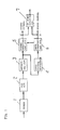
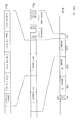
- FIG. 1 denotes the tuner of a television receiver
- 2 is a VIF circuit
- 3 is a detecting circuit
- 4 is a circuit to reproduce synchronising signals
- 5 is a circuit to change over whether or not to invert the video signal on the basis of the data processing result of a data processing circuit 6.
- This data processing circuit 6 is intended to process the data, convert digital sound into analog signal, and deliver a discriminating signal (changeover signal) to determine whether or not to invert the video signal.
- Numeral 7 is a circuit to form a signal of RF (VHF) using the sound and image normalized in a remodulation circuit of RF as the inputs.
- VHF signal of RF
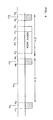
- the output of the detecting circuit 3 lacks horizontal synchronizing signal and vertical synchronizing signal as shown in Fig. 2 ⁇ 1 , Fig. 3 4)22, ⁇ 24 , and vertical trigger signal V T and horizontal trigger signal H T are inserted instead.
- the shaded areas 4)22, 4) 23 in Fig. 3 are in same composition as t 2 to t 6 in Fig. 2 ⁇ 1 .
- the polarity of the video signal is repeatedly inverted and noninverted at random intervals in the unit of horizontal scanning line unit or screen unit. When the polarity of color burst signal is changed, however, hue deviation or other problems may occur. Therefore, the color burst signal is not inverted.
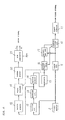
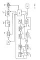
- a buffer 8 is sliced in a slicing circuit 12 and shaped into a binary signal, and is sampled in a sampling circuit 13 to store sound data at every H in a buffer memory 18, while the delta-encoded signal is decoded in a delta decoder 19 and transferred into a buffer memory 20, of which output is D-A converted at a speed of 2 f H by D/A converter 21, and two outputs for right and left are obtained using the high quality sound of sampling rate 2f H and maximum frequency f H as the output of D/A converter 21.
- the data of 5H to 7H, 268H to 270H in Fig. 3 are written into a buffer memory 14, read out, and decoded in a decoder 15, and a signal to determine whether or not to invert the video signal is delivered, while a pulse to determing the inverting period is formed in an inverting changeover circuit 16 and applied to a synthesizing circuit 10.
- the output of a clamp circuit 9 is inverted in an inverting amplifier 17, of which output is also applied to the synthesizing circuit 10, and the output of the synthesizing circuit 10 is changed over whether the output of clamp circuit 9 or the output of the inverting amplifier 17 is applied, by the output of the inverting changeover circuit 16.
- the output of the inverting changeover circuit 16 is also applied to the inverting amplifier 17, and the output of the inverting amplifier 17 is suppressed when inversion is not required, and the crosstalk is lessened in the synthesizing circuit 10.
- the output of the synthesizing circuit 10 is clamped in a clamp circuit 11, an ordinary video signal is obtained.
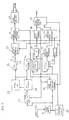
- Fig. 5 a detecting circuit of vertical trigger signal V T
- horizontal trigger signal H T 23
- 24 is a circuit for effecting PLL (phase locked loop) of 6f sc and f sc of VCO (voltage controlled oscillator)
- 26 is a 1/10 divider
- 27 is a 1/3 divider
- 28 is a 1/455 divider of the output of 1/3 divider 27, that is, 4f sc , of which output is 2f H .
- Numeral 29 is a 1/2 divider, of which output is f H , and 30 is a 1/525 divider of 2f H , of which output is about 60 Hz.
- Numeral 31 is an equalizing pulse generator, and 32 is a generator of vertical synchronizing signal.
- Numeral 28 through 32 are known circuits as the synchronizing board of TV signals.
- Numeral 33 is a sampling clock forming circuit, and when the data transmission rate is 6/5f sc , a sampling clock is formed by using 12/5f sc of the output of the 1/5 divider 26. The output of the sampling clock forming circuit 33 is applied to a data sampling processing circuit 6 to be sampled, and the data is processed.
- Numeral 6A is a sound reproducing circuit for forming analog sound.
- Numeral 34 is a burst gate forming circuit for forming a burst gate from the output of the 1/2 divider 29.
- a synchronous reproducing circuit 35 composite synchronizing signals are formed from the outputs of dividers 29, 31, 32, and the composite synchronizing signal output of this circuit 35 and the output of video clamp, inverting circuit 36 are synthesized in a video synthesizing circuit 37, and a video signal is formed.
- the video clamp, inverting circuit 36 clamps the video signal, and inverts the video signal for a required period according to the output of the data sampling processing circuit 6.
- the synchronizing signal is established, the data is processed, and the sound is processed.
- a total of 44 bits comprising two samples each at the right and left are sent forth every H, and a phase matching circuit for 1, 0 is provided before it.
- 45 clock pulses are generated thereafter from 0 to 44 .
- the phase of ⁇ 13 is adjusted so that the 1/5 divider 26 may be reset at the first bit of ⁇ 12 , the time for ⁇ 12 settles within the portion of one cycle of 12f sc , that is, about 23 ns ( ⁇ 11.5 ns).
- FIG. 8 An example of sampling and sound signal processing circuit is shown in Fig. 8.
- the output of the buffer 8 is sliced in a slicing circuit 38, and a binary waveform as shown in Fig. 7 ⁇ 12 , is obtained.
- a timing control circuit 40 gate pulses containing a portion of sound signal (t 2 to t 6 in Fig. 2) are generated from the outputs of 1/2 divider 29 and 1/525 divider 30, and are applied to an AND gate 39, and only the sound signals are extracted and applied to D terminal of D flip-flop 41.
- the D flip-flop 41 is clocked by Fig. 7 ⁇ 13 , the data can be sampled.
- the fall of t 42 is detected by the output of the AND gate 39, and clocks 0 to 44 are generated as stated above.
- the buffer memory 43 is controlled by the timing control circuit 40 so that the output of the D flip-flop 41 may be fed to the buffer memory 43 only for the portion of 44 bits of 1 to 44 .
- a control signal is sent from the timing control circuit 40 to the buffer memory 42 so that data for the portion of 440 bits may be stored.
- the data of T 32 to T 33 is stored in the buffer memory 43 somewhat later (for example, 1 us) than T 33 .
- the data of ao to a 1 and the previous data are arithmetically operated within, for example, 1 us, from T 33 + ⁇ T.
- both operations can be processed within 1 us each.
- the result of this arithmetic operation is D-A converted by the D-A converter 45 and stored in memory L 1 of 47.
- the data of co to C 10 is compared with the previous data, and the result is D-A converted and stored in memory R 1 of 49.
- Numerals 47 through 50 are analog memories.
- each memory of 47 to 50 is alternately delivered from AND gates 51 to 55 and OR gates 53, 56. That is, in T 3x to T 3 y, since the output of timing control circuit 40 is at low level, the output of the inverter 46 becomes high level, and AND gates 51, 54 are made to conduct, so that the contents of memories 47, 49 may be taken out as L and R sounds, respectively. In T 3 y to T 4x , since the output of timing control circuit 40 is at high level, the AND gates 52, 55 are made to conduct, and the outputs of memories 48, 50 becomes L and R outputs. The operation is the same for other Hs.
- the sound data received at time T 34 to T 35 is processed until T 39 , and is fed to an arithmetic operation circuit 44 at T 42 , and, at this time, 11 bits each of L 1 , R 1 of T 42 to T 43 are ignored, and are directly D-A converted.
- the data sent within T 34 to T 35 in Fig. 9 is delivered. That is, uncompressed data is used only for one sample in every field. Thereafter, taking this value as the starting value, only the change portion is successively added or subtracted as described above. Meanwhile, if the first one bit of 11 bits is treated as a code, the remaining 10 bits are increments or decrements. Therefore, it is possible to follow up the changes of 60 dB.
- the reference value can be transmitted once in every field correctly by adding an error correction code even in a so-called digital enconding of 11 bits, so that the sound signals are of sufficient integrity and resistant to noise.
- Numerals 57, 58 in Fig. 8 are parts of signal processing circuit used in a so-called teletext receiver or the like, and 57 is a bus buffer and 58 is a CPU.
- the data in the VBL after 4H in Fig. 3 is processed in these bus buffer 57 and CPU 58, of which composition is known, being similar to that of a so-called teletext receiver.
- Fig. 9 An accurate reproduction of the reference value of sound is described below while referring to Figs. 9 to 11.
- the actual sound data in Fig. 9 is assumed as shown in Fig. 10.
- the preceding 32 bits are composed of 24 repetitive bits of 1 and 0 of clock run (CR) and 9 bits of framing code.
- the next 384 bits consist of three sets of sound data of 128 bits each, having the same content, comprising 64 bits of information and 64 bits of check code as in ⁇ 101 . This takes the form of source BCH code, and can correct random and burst error within 10 bits.
- the final 24 bits of ⁇ 100 are CRC codes.
- the 8-bit data may be used as required, and CRC may not be necessarily used.
- Numeral 57 is an analog gate, and gate pulses comprising T 34 to T 39 in 4H in Fig. 9 are generated in the timing control 40, and the output of video buffer 8 is gated. If any data of the same number of bits is wholly superposed, for example, up to 21 H in VBL, gate pulses including T 34 to T 39 (440 bits) are delivered every H from the timing control circuit 40 from 4H to 21 H and 267H to 284H, and are applied to a gate 57. The output of the gate 57 is converted into a binary value in the slicing circuit 38, and is gated by the output of the timing control circuit 40 at AND gate 39'. The AND gate 39', different from the gate 39 in Fig.
- a sampling circuit 41' is a shift register having an S-P converting function.
- the output of gate 57 is applied to BPA 58 of 6/5f sc , and the part of clock run-in in Fig. 10 ⁇ 101 appears as sine wave.
- This is used to control the phase of the output of VCO 59 of 12/5f sc .
- Numeral 60 is a phase shifter, and the phase of the output of VCO 59 is matched with the phase of the output of BPA 58 by the output of BPA 58, that is, the rise or fall of the output of the phase shifter 60 is adjusted to the middle of each bit of received ⁇ 101 , and after the clock run period, phase information is not received but is held until the clock run of next horizontal scanning period or clock run of next field.
- phase shifter 60 since at least 1 H can be sufficiently maintained within a same phase, a clock synchronized with data can be formed in the phase shifter 60.
- the circuit of phase shifter 60 is an analog one, and its output is shaped into pulses in a shaping circuit 61, and supplied into a clock generating circuit 62.
- the output of the sampling circuit 41' is latched by every 8 bits, and is supplied into the buffer memory 57. Data for the portion of two fields is stored in the buffer memory 57.
- Writing and reading of data into the buffer memory 57 are controlled in W/R processing circuit 63.
- the contents in the buffer memory that is, the data in the corresponding field (the portion of three times of L 100 , R 100 in Fig. 10 ⁇ 102 ) of 2 x 56 x 3 bits for the portion of two fields are compared.
- L 101 , R 101 are determined. If not determined, the L 100 , R 100 stored in the previous field are used.
- the L 101 , R, 0 are held up to the next field.
- the output of the CPU is stored in the buffer memory 65, and applied to the arithmetic operation circuit 44 before T 4x to be used as the reference value at the time of T 4 y, and is also D-A converted and stored in memories 47, 49 before T 4x .
- the reference values of L and R are obtained once in every field without being compressed, the operation returns to a normal state within one field if malfunction occurs during delta decoding.
- this invention presents a processing circuit for delivering sound of high quality containing reproduced image, which is hard to be illegally accessed, in decoding encoded sound signals. It is another advantage that the decoding circuit is suited to LSI and is practical.
- the above disclosure is based on a 525 line television system but is equally applicable to other systems e.g. 625 line or 1050 line systems.
Claims (7)
dadurch gekennzeichnet, daß die Hilfsmittel (8, 30, 33, 38 bis 41, 43) eine Einrichtung zum Empfang deltamodulierter, verdichteter, digitaler Tonsignalet Ax enthalten, die in der horizontalen Austastperiode des Fernsehsignals überlagert sind, und ferner gekennzeichnet
Applications Claiming Priority (4)
| Application Number | Priority Date | Filing Date | Title |
|---|---|---|---|
| JP59026337A JPS60171882A (ja) | 1984-02-15 | 1984-02-15 | デイジタル音声受信装置 |
| JP26337/84 | 1984-02-15 | ||
| JP59026334A JPS60171881A (ja) | 1984-02-15 | 1984-02-15 | 音声信号処理装置 |
| JP26334/84 | 1984-02-15 |
Publications (3)
| Publication Number | Publication Date |
|---|---|
| EP0152309A2 EP0152309A2 (de) | 1985-08-21 |
| EP0152309A3 EP0152309A3 (en) | 1987-08-05 |
| EP0152309B1 true EP0152309B1 (de) | 1992-01-22 |
Family
ID=26364099
Family Applications (1)
| Application Number | Title | Priority Date | Filing Date |
|---|---|---|---|
| EP85301026A Expired EP0152309B1 (de) | 1984-02-15 | 1985-02-15 | Vorrichtung zum Verarbeiten eines Fernsehaudiosignals |
Country Status (5)
| Country | Link |
|---|---|
| US (1) | US4745476A (de) |
| EP (1) | EP0152309B1 (de) |
| AU (1) | AU560508B2 (de) |
| CA (1) | CA1237193A (de) |
| DE (1) | DE3585237D1 (de) |
Cited By (1)
| Publication number | Priority date | Publication date | Assignee | Title |
|---|---|---|---|---|
| US6710811B1 (en) | 1998-05-09 | 2004-03-23 | Thomson Licensing S.A. | Data processing device |
Families Citing this family (17)
| Publication number | Priority date | Publication date | Assignee | Title |
|---|---|---|---|---|
| US5177604A (en) * | 1986-05-14 | 1993-01-05 | Radio Telcom & Technology, Inc. | Interactive television and data transmission system |
| US4821097A (en) * | 1987-03-05 | 1989-04-11 | General Instrument Corporation | Apparatus and method for providing digital audio on the sound carrier of a standard television signal |
| JPH0396180A (ja) * | 1989-09-08 | 1991-04-22 | Sony Corp | 受信装置 |
| US5387941A (en) * | 1991-06-14 | 1995-02-07 | Wavephore, Inc. | Data with video transmitter |
| US5559559A (en) * | 1991-06-14 | 1996-09-24 | Wavephore, Inc. | Transmitting a secondary signal with dynamic injection level control |
| US5327237A (en) * | 1991-06-14 | 1994-07-05 | Wavephore, Inc. | Transmitting data with video |
| US5831679A (en) * | 1991-06-14 | 1998-11-03 | Wavephore, Inc. | Network for retrieval and video transmission of information |
| US5410360A (en) * | 1991-06-14 | 1995-04-25 | Wavephore, Inc. | Timing control for injecting a burst and data into a video signal |
| US5617148A (en) * | 1991-06-14 | 1997-04-01 | Wavephore, Inc. | Filter by-pass for transmitting an additional signal with a video signal |
| JP3235903B2 (ja) * | 1992-06-11 | 2001-12-04 | 株式会社リコー | スチルカメラ |
| CA2100322C (en) * | 1992-08-06 | 2004-06-22 | Christoph Eisenbarth | Method and apparatus for monitoring image processing operations |
| US5426466A (en) * | 1992-12-31 | 1995-06-20 | Emhiser Research Limited | Composite video signal with audio |
| US7110658B1 (en) * | 1993-01-08 | 2006-09-19 | Televentions, Llc | Method and apparatus for eliminating television commercial messages |
| US5455630A (en) * | 1993-08-06 | 1995-10-03 | Arthur D. Little Enterprises, Inc. | Method and apparatus for inserting digital data in a blanking interval of an RF modulated video signal |
| US5692093A (en) * | 1993-01-08 | 1997-11-25 | Srt, Inc. | Method and apparatus for eliminating television commercial messages |
| NL1000025C2 (nl) * | 1995-04-05 | 1996-10-04 | Tratec Telecom B V | Schakeling voor het op digitale wijze verwerken van electrische signalen afkomstig van meerdere audiokanalen. |
| US5751366A (en) * | 1995-08-31 | 1998-05-12 | Lucent Technologies Inc. | Inclusion of audio signal within video signal |
Family Cites Families (3)
| Publication number | Priority date | Publication date | Assignee | Title |
|---|---|---|---|---|
| IL58735A (en) * | 1978-12-04 | 1982-01-31 | Oak Industries Inc | Subscription television coding system |
| US4424532A (en) * | 1980-05-14 | 1984-01-03 | Oak Industries Inc. | Coding and decoding system for video and audio signals |
| FR2538645B1 (fr) * | 1982-12-28 | 1986-04-11 | Thomson Csf | Procede et dispositif d'interpolation de la parole dans un systeme de transmission de parole numerisee |
-
1985
- 1985-02-12 US US06/701,284 patent/US4745476A/en not_active Expired - Lifetime
- 1985-02-12 AU AU38641/85A patent/AU560508B2/en not_active Ceased
- 1985-02-14 CA CA000474276A patent/CA1237193A/en not_active Expired
- 1985-02-15 DE DE8585301026T patent/DE3585237D1/de not_active Expired - Lifetime
- 1985-02-15 EP EP85301026A patent/EP0152309B1/de not_active Expired
Cited By (1)
| Publication number | Priority date | Publication date | Assignee | Title |
|---|---|---|---|---|
| US6710811B1 (en) | 1998-05-09 | 2004-03-23 | Thomson Licensing S.A. | Data processing device |
Also Published As
| Publication number | Publication date |
|---|---|
| AU3864185A (en) | 1985-08-22 |
| US4745476A (en) | 1988-05-17 |
| AU560508B2 (en) | 1987-04-09 |
| CA1237193A (en) | 1988-05-24 |
| DE3585237D1 (de) | 1992-03-05 |
| EP0152309A3 (en) | 1987-08-05 |
| EP0152309A2 (de) | 1985-08-21 |
Similar Documents
| Publication | Publication Date | Title |
|---|---|---|
| EP0152309B1 (de) | Vorrichtung zum Verarbeiten eines Fernsehaudiosignals | |
| JP3546889B2 (ja) | 多重化伝送方法および装置 | |
| EP0574892B1 (de) | Vorrichtung zum Aufzeichnen/Wiedergeben eines digitalen Videosignals | |
| US5410360A (en) | Timing control for injecting a burst and data into a video signal | |
| US6072872A (en) | Determination of scrambling mode of a television signal | |
| GB2077547A (en) | A coding and decoding system for video and audio signals | |
| US4068265A (en) | Method and apparatus for sampling and reproducing television information | |
| JPH0666773B2 (ja) | 通信システムにおける同期再生 | |
| US4839922A (en) | CATV scrambling and descrambling method | |
| GB2038137A (en) | Coding and decoding of TV signals | |
| US4488176A (en) | Method of and apparatus for modifying a video signal to inhibit recording thereof | |
| US4673975A (en) | Television signal scrambling apparatus | |
| EP0973329B1 (de) | HDTV-Rahmensynchronisierungssystem ,das ein sauberes digitales Signal liefert ohne variable Verzögerung | |
| CA1205900A (en) | Scrambling system of television signal | |
| US5381186A (en) | Video signal decoder muting circuit and method of muting | |
| US3903356A (en) | Apparatus for reproducing synchronizing signals | |
| EP0119751B1 (de) | Verfahren zum Verwürfeln von Fernsehsignalen | |
| US5196921A (en) | Data transmission using color burst position modulation | |
| EP0734169B1 (de) | Schaltung zur Verarbeitung eines Fernsehsignals | |
| EP0853431B1 (de) | Signalverarbeitungsanlage | |
| US5099312A (en) | Timebase corrector | |
| JPH0652946B2 (ja) | デスクランブル装置 | |
| Kano et al. | Television frame synchronizer | |
| PL173671B1 (pl) | Sposób oraz układ do dekodowania rozszerzonego sygnału telewizyjnego | |
| CA1248625A (en) | Key signal transmitting method for scrambling a tv picture |
Legal Events
| Date | Code | Title | Description |
|---|---|---|---|
| PUAI | Public reference made under article 153(3) epc to a published international application that has entered the european phase |
Free format text: ORIGINAL CODE: 0009012 |
|
| AK | Designated contracting states |
Designated state(s): DE FR GB |
|
| PUAL | Search report despatched |
Free format text: ORIGINAL CODE: 0009013 |
|
| AK | Designated contracting states |
Kind code of ref document: A3 Designated state(s): DE FR GB |
|
| 17P | Request for examination filed |
Effective date: 19871020 |
|
| 17Q | First examination report despatched |
Effective date: 19900226 |
|
| GRAA | (expected) grant |
Free format text: ORIGINAL CODE: 0009210 |
|
| AK | Designated contracting states |
Kind code of ref document: B1 Designated state(s): DE FR GB |
|
| REF | Corresponds to: |
Ref document number: 3585237 Country of ref document: DE Date of ref document: 19920305 |
|
| ET | Fr: translation filed | ||
| PLBE | No opposition filed within time limit |
Free format text: ORIGINAL CODE: 0009261 |
|
| STAA | Information on the status of an ep patent application or granted ep patent |
Free format text: STATUS: NO OPPOSITION FILED WITHIN TIME LIMIT |
|
| 26N | No opposition filed | ||
| REG | Reference to a national code |
Ref country code: GB Ref legal event code: 746 Effective date: 19950224 |
|
| REG | Reference to a national code |
Ref country code: FR Ref legal event code: D6 |
|
| PGFP | Annual fee paid to national office [announced via postgrant information from national office to epo] |
Ref country code: GB Payment date: 19980206 Year of fee payment: 14 |
|
| PGFP | Annual fee paid to national office [announced via postgrant information from national office to epo] |
Ref country code: FR Payment date: 19980210 Year of fee payment: 14 |
|
| PGFP | Annual fee paid to national office [announced via postgrant information from national office to epo] |
Ref country code: DE Payment date: 19980220 Year of fee payment: 14 |
|
| PG25 | Lapsed in a contracting state [announced via postgrant information from national office to epo] |
Ref country code: GB Free format text: LAPSE BECAUSE OF NON-PAYMENT OF DUE FEES Effective date: 19990215 |
|
| GBPC | Gb: european patent ceased through non-payment of renewal fee |
Effective date: 19990215 |
|
| PG25 | Lapsed in a contracting state [announced via postgrant information from national office to epo] |
Ref country code: FR Free format text: LAPSE BECAUSE OF NON-PAYMENT OF DUE FEES Effective date: 19991029 |
|
| PG25 | Lapsed in a contracting state [announced via postgrant information from national office to epo] |
Ref country code: DE Free format text: LAPSE BECAUSE OF NON-PAYMENT OF DUE FEES Effective date: 19991201 |
|
| REG | Reference to a national code |
Ref country code: FR Ref legal event code: ST |