EP0148083A2 - Ultra-high speed semiconductor integrated circuit device having a multi-layered wiring board - Google Patents
Ultra-high speed semiconductor integrated circuit device having a multi-layered wiring board Download PDFInfo
- Publication number
- EP0148083A2 EP0148083A2 EP84402696A EP84402696A EP0148083A2 EP 0148083 A2 EP0148083 A2 EP 0148083A2 EP 84402696 A EP84402696 A EP 84402696A EP 84402696 A EP84402696 A EP 84402696A EP 0148083 A2 EP0148083 A2 EP 0148083A2
- Authority
- EP
- European Patent Office
- Prior art keywords
- wiring board
- integrated circuit
- circuit device
- semiconductor integrated
- chip
- Prior art date
- Legal status (The legal status is an assumption and is not a legal conclusion. Google has not performed a legal analysis and makes no representation as to the accuracy of the status listed.)
- Granted
Links
Images

Classifications
-
- H—ELECTRICITY
- H01—ELECTRIC ELEMENTS
- H01L—SEMICONDUCTOR DEVICES NOT COVERED BY CLASS H10
- H01L24/00—Arrangements for connecting or disconnecting semiconductor or solid-state bodies; Methods or apparatus related thereto
- H01L24/01—Means for bonding being attached to, or being formed on, the surface to be connected, e.g. chip-to-package, die-attach, "first-level" interconnects; Manufacturing methods related thereto
- H01L24/50—Tape automated bonding [TAB] connectors, i.e. film carriers; Manufacturing methods related thereto
-
- H—ELECTRICITY
- H01—ELECTRIC ELEMENTS
- H01L—SEMICONDUCTOR DEVICES NOT COVERED BY CLASS H10
- H01L21/00—Processes or apparatus adapted for the manufacture or treatment of semiconductor or solid state devices or of parts thereof
- H01L21/02—Manufacture or treatment of semiconductor devices or of parts thereof
- H01L21/04—Manufacture or treatment of semiconductor devices or of parts thereof the devices having at least one potential-jump barrier or surface barrier, e.g. PN junction, depletion layer or carrier concentration layer
- H01L21/50—Assembly of semiconductor devices using processes or apparatus not provided for in a single one of the subgroups H01L21/06 - H01L21/326, e.g. sealing of a cap to a base of a container
- H01L21/60—Attaching or detaching leads or other conductive members, to be used for carrying current to or from the device in operation
-
- H—ELECTRICITY
- H01—ELECTRIC ELEMENTS
- H01L—SEMICONDUCTOR DEVICES NOT COVERED BY CLASS H10
- H01L23/00—Details of semiconductor or other solid state devices
- H01L23/48—Arrangements for conducting electric current to or from the solid state body in operation, e.g. leads, terminal arrangements ; Selection of materials therefor
- H01L23/488—Arrangements for conducting electric current to or from the solid state body in operation, e.g. leads, terminal arrangements ; Selection of materials therefor consisting of soldered or bonded constructions
- H01L23/498—Leads, i.e. metallisations or lead-frames on insulating substrates, e.g. chip carriers
-
- H—ELECTRICITY
- H01—ELECTRIC ELEMENTS
- H01L—SEMICONDUCTOR DEVICES NOT COVERED BY CLASS H10
- H01L23/00—Details of semiconductor or other solid state devices
- H01L23/58—Structural electrical arrangements for semiconductor devices not otherwise provided for, e.g. in combination with batteries
- H01L23/64—Impedance arrangements
- H01L23/66—High-frequency adaptations
-
- H—ELECTRICITY
- H01—ELECTRIC ELEMENTS
- H01L—SEMICONDUCTOR DEVICES NOT COVERED BY CLASS H10
- H01L2224/00—Indexing scheme for arrangements for connecting or disconnecting semiconductor or solid-state bodies and methods related thereto as covered by H01L24/00
- H01L2224/01—Means for bonding being attached to, or being formed on, the surface to be connected, e.g. chip-to-package, die-attach, "first-level" interconnects; Manufacturing methods related thereto
- H01L2224/42—Wire connectors; Manufacturing methods related thereto
- H01L2224/47—Structure, shape, material or disposition of the wire connectors after the connecting process
- H01L2224/48—Structure, shape, material or disposition of the wire connectors after the connecting process of an individual wire connector
- H01L2224/4805—Shape
- H01L2224/4809—Loop shape
- H01L2224/48091—Arched
-
- H—ELECTRICITY
- H01—ELECTRIC ELEMENTS
- H01L—SEMICONDUCTOR DEVICES NOT COVERED BY CLASS H10
- H01L2224/00—Indexing scheme for arrangements for connecting or disconnecting semiconductor or solid-state bodies and methods related thereto as covered by H01L24/00
- H01L2224/01—Means for bonding being attached to, or being formed on, the surface to be connected, e.g. chip-to-package, die-attach, "first-level" interconnects; Manufacturing methods related thereto
- H01L2224/42—Wire connectors; Manufacturing methods related thereto
- H01L2224/47—Structure, shape, material or disposition of the wire connectors after the connecting process
- H01L2224/48—Structure, shape, material or disposition of the wire connectors after the connecting process of an individual wire connector
- H01L2224/481—Disposition
- H01L2224/48151—Connecting between a semiconductor or solid-state body and an item not being a semiconductor or solid-state body, e.g. chip-to-substrate, chip-to-passive
- H01L2224/48221—Connecting between a semiconductor or solid-state body and an item not being a semiconductor or solid-state body, e.g. chip-to-substrate, chip-to-passive the body and the item being stacked
- H01L2224/48225—Connecting between a semiconductor or solid-state body and an item not being a semiconductor or solid-state body, e.g. chip-to-substrate, chip-to-passive the body and the item being stacked the item being non-metallic, e.g. insulating substrate with or without metallisation
- H01L2224/48227—Connecting between a semiconductor or solid-state body and an item not being a semiconductor or solid-state body, e.g. chip-to-substrate, chip-to-passive the body and the item being stacked the item being non-metallic, e.g. insulating substrate with or without metallisation connecting the wire to a bond pad of the item
-
- H—ELECTRICITY
- H01—ELECTRIC ELEMENTS
- H01L—SEMICONDUCTOR DEVICES NOT COVERED BY CLASS H10
- H01L24/00—Arrangements for connecting or disconnecting semiconductor or solid-state bodies; Methods or apparatus related thereto
- H01L24/01—Means for bonding being attached to, or being formed on, the surface to be connected, e.g. chip-to-package, die-attach, "first-level" interconnects; Manufacturing methods related thereto
- H01L24/42—Wire connectors; Manufacturing methods related thereto
- H01L24/47—Structure, shape, material or disposition of the wire connectors after the connecting process
- H01L24/48—Structure, shape, material or disposition of the wire connectors after the connecting process of an individual wire connector
-
- H—ELECTRICITY
- H01—ELECTRIC ELEMENTS
- H01L—SEMICONDUCTOR DEVICES NOT COVERED BY CLASS H10
- H01L2924/00—Indexing scheme for arrangements or methods for connecting or disconnecting semiconductor or solid-state bodies as covered by H01L24/00
- H01L2924/0001—Technical content checked by a classifier
- H01L2924/00014—Technical content checked by a classifier the subject-matter covered by the group, the symbol of which is combined with the symbol of this group, being disclosed without further technical details
-
- H—ELECTRICITY
- H01—ELECTRIC ELEMENTS
- H01L—SEMICONDUCTOR DEVICES NOT COVERED BY CLASS H10
- H01L2924/00—Indexing scheme for arrangements or methods for connecting or disconnecting semiconductor or solid-state bodies as covered by H01L24/00
- H01L2924/01—Chemical elements
- H01L2924/01006—Carbon [C]
-
- H—ELECTRICITY
- H01—ELECTRIC ELEMENTS
- H01L—SEMICONDUCTOR DEVICES NOT COVERED BY CLASS H10
- H01L2924/00—Indexing scheme for arrangements or methods for connecting or disconnecting semiconductor or solid-state bodies as covered by H01L24/00
- H01L2924/01—Chemical elements
- H01L2924/01019—Potassium [K]
-
- H—ELECTRICITY
- H01—ELECTRIC ELEMENTS
- H01L—SEMICONDUCTOR DEVICES NOT COVERED BY CLASS H10
- H01L2924/00—Indexing scheme for arrangements or methods for connecting or disconnecting semiconductor or solid-state bodies as covered by H01L24/00
- H01L2924/01—Chemical elements
- H01L2924/01029—Copper [Cu]
-
- H—ELECTRICITY
- H01—ELECTRIC ELEMENTS
- H01L—SEMICONDUCTOR DEVICES NOT COVERED BY CLASS H10
- H01L2924/00—Indexing scheme for arrangements or methods for connecting or disconnecting semiconductor or solid-state bodies as covered by H01L24/00
- H01L2924/01—Chemical elements
- H01L2924/01033—Arsenic [As]
-
- H—ELECTRICITY
- H01—ELECTRIC ELEMENTS
- H01L—SEMICONDUCTOR DEVICES NOT COVERED BY CLASS H10
- H01L2924/00—Indexing scheme for arrangements or methods for connecting or disconnecting semiconductor or solid-state bodies as covered by H01L24/00
- H01L2924/01—Chemical elements
- H01L2924/01047—Silver [Ag]
-
- H—ELECTRICITY
- H01—ELECTRIC ELEMENTS
- H01L—SEMICONDUCTOR DEVICES NOT COVERED BY CLASS H10
- H01L2924/00—Indexing scheme for arrangements or methods for connecting or disconnecting semiconductor or solid-state bodies as covered by H01L24/00
- H01L2924/01—Chemical elements
- H01L2924/01061—Promethium [Pm]
-
- H—ELECTRICITY
- H01—ELECTRIC ELEMENTS
- H01L—SEMICONDUCTOR DEVICES NOT COVERED BY CLASS H10
- H01L2924/00—Indexing scheme for arrangements or methods for connecting or disconnecting semiconductor or solid-state bodies as covered by H01L24/00
- H01L2924/01—Chemical elements
- H01L2924/01074—Tungsten [W]
-
- H—ELECTRICITY
- H01—ELECTRIC ELEMENTS
- H01L—SEMICONDUCTOR DEVICES NOT COVERED BY CLASS H10
- H01L2924/00—Indexing scheme for arrangements or methods for connecting or disconnecting semiconductor or solid-state bodies as covered by H01L24/00
- H01L2924/01—Chemical elements
- H01L2924/01079—Gold [Au]
-
- H—ELECTRICITY
- H01—ELECTRIC ELEMENTS
- H01L—SEMICONDUCTOR DEVICES NOT COVERED BY CLASS H10
- H01L2924/00—Indexing scheme for arrangements or methods for connecting or disconnecting semiconductor or solid-state bodies as covered by H01L24/00
- H01L2924/01—Chemical elements
- H01L2924/01082—Lead [Pb]
-
- H—ELECTRICITY
- H01—ELECTRIC ELEMENTS
- H01L—SEMICONDUCTOR DEVICES NOT COVERED BY CLASS H10
- H01L2924/00—Indexing scheme for arrangements or methods for connecting or disconnecting semiconductor or solid-state bodies as covered by H01L24/00
- H01L2924/10—Details of semiconductor or other solid state devices to be connected
- H01L2924/102—Material of the semiconductor or solid state bodies
- H01L2924/1025—Semiconducting materials
- H01L2924/1026—Compound semiconductors
- H01L2924/1032—III-V
- H01L2924/10329—Gallium arsenide [GaAs]
-
- H—ELECTRICITY
- H01—ELECTRIC ELEMENTS
- H01L—SEMICONDUCTOR DEVICES NOT COVERED BY CLASS H10
- H01L2924/00—Indexing scheme for arrangements or methods for connecting or disconnecting semiconductor or solid-state bodies as covered by H01L24/00
- H01L2924/10—Details of semiconductor or other solid state devices to be connected
- H01L2924/11—Device type
- H01L2924/14—Integrated circuits
-
- H—ELECTRICITY
- H01—ELECTRIC ELEMENTS
- H01L—SEMICONDUCTOR DEVICES NOT COVERED BY CLASS H10
- H01L2924/00—Indexing scheme for arrangements or methods for connecting or disconnecting semiconductor or solid-state bodies as covered by H01L24/00
- H01L2924/15—Details of package parts other than the semiconductor or other solid state devices to be connected
- H01L2924/151—Die mounting substrate
- H01L2924/1515—Shape
- H01L2924/15153—Shape the die mounting substrate comprising a recess for hosting the device
-
- H—ELECTRICITY
- H01—ELECTRIC ELEMENTS
- H01L—SEMICONDUCTOR DEVICES NOT COVERED BY CLASS H10
- H01L2924/00—Indexing scheme for arrangements or methods for connecting or disconnecting semiconductor or solid-state bodies as covered by H01L24/00
- H01L2924/15—Details of package parts other than the semiconductor or other solid state devices to be connected
- H01L2924/151—Die mounting substrate
- H01L2924/15165—Monolayer substrate
-
- H—ELECTRICITY
- H01—ELECTRIC ELEMENTS
- H01L—SEMICONDUCTOR DEVICES NOT COVERED BY CLASS H10
- H01L2924/00—Indexing scheme for arrangements or methods for connecting or disconnecting semiconductor or solid-state bodies as covered by H01L24/00
- H01L2924/15—Details of package parts other than the semiconductor or other solid state devices to be connected
- H01L2924/151—Die mounting substrate
- H01L2924/1517—Multilayer substrate
-
- H—ELECTRICITY
- H01—ELECTRIC ELEMENTS
- H01L—SEMICONDUCTOR DEVICES NOT COVERED BY CLASS H10
- H01L2924/00—Indexing scheme for arrangements or methods for connecting or disconnecting semiconductor or solid-state bodies as covered by H01L24/00
- H01L2924/15—Details of package parts other than the semiconductor or other solid state devices to be connected
- H01L2924/151—Die mounting substrate
- H01L2924/153—Connection portion
- H01L2924/1531—Connection portion the connection portion being formed only on the surface of the substrate opposite to the die mounting surface
- H01L2924/15312—Connection portion the connection portion being formed only on the surface of the substrate opposite to the die mounting surface being a pin array, e.g. PGA
-
- H—ELECTRICITY
- H01—ELECTRIC ELEMENTS
- H01L—SEMICONDUCTOR DEVICES NOT COVERED BY CLASS H10
- H01L2924/00—Indexing scheme for arrangements or methods for connecting or disconnecting semiconductor or solid-state bodies as covered by H01L24/00
- H01L2924/15—Details of package parts other than the semiconductor or other solid state devices to be connected
- H01L2924/161—Cap
- H01L2924/1615—Shape
- H01L2924/16195—Flat cap [not enclosing an internal cavity]
-
- H—ELECTRICITY
- H01—ELECTRIC ELEMENTS
- H01L—SEMICONDUCTOR DEVICES NOT COVERED BY CLASS H10
- H01L2924/00—Indexing scheme for arrangements or methods for connecting or disconnecting semiconductor or solid-state bodies as covered by H01L24/00
- H01L2924/19—Details of hybrid assemblies other than the semiconductor or other solid state devices to be connected
- H01L2924/1901—Structure
- H01L2924/1904—Component type
- H01L2924/19041—Component type being a capacitor
-
- H—ELECTRICITY
- H01—ELECTRIC ELEMENTS
- H01L—SEMICONDUCTOR DEVICES NOT COVERED BY CLASS H10
- H01L2924/00—Indexing scheme for arrangements or methods for connecting or disconnecting semiconductor or solid-state bodies as covered by H01L24/00
- H01L2924/30—Technical effects
- H01L2924/301—Electrical effects
- H01L2924/3011—Impedance
-
- H—ELECTRICITY
- H01—ELECTRIC ELEMENTS
- H01L—SEMICONDUCTOR DEVICES NOT COVERED BY CLASS H10
- H01L2924/00—Indexing scheme for arrangements or methods for connecting or disconnecting semiconductor or solid-state bodies as covered by H01L24/00
- H01L2924/30—Technical effects
- H01L2924/301—Electrical effects
- H01L2924/3025—Electromagnetic shielding
Definitions
- This invention relates to a semiconductor integrated circuit device, and, more particularly, to a layout and connecting structure between inner lead terminals of a package and bonding pads on a chip for an ultra-high speed semiconductor integrated circuit device.
- GaAs gallium arsenide
- Gbit/s gigabits per second
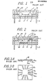
- Figures 1 and 2 are schematical cross-sectional views of prior art structures of semiconductor IC devices such as GaAs IC devices.
- reference numerals 1 and 11 designate packages
- 2 and 12 are semiconductor chips mounted in the packages 1 and 11, 3 and 13 are outer loads
- 4 and 14 are inner lead terminals connected to the outer leads
- 5 and 15 are bonding pads
- 7 and 17 are cover plates which cover the packages 1 and 11.
- the GaAs substrate chip 2, 12 is located in a cavity 50 of the package 1, 11 and is bonded to the ceramic package by means of a low melting point metal sheet 6 0 .
- the chip size is for example approximately 4 mm square.
- a hermetic seal 70 is provided for hermetically sealing the cover plate 7, 17 to the package 1, 11.
- inner leads 6 are provided for connecting the bonding pads 5 to respective outer leads 3 through the inner lead terminals 4.
- a wiring board 16 having a printed wiring circuit is provided for connecting the bonding pads 15 to respective outer leads 13 through the inner lead terminals 14.
- Figures 3A and 3B are respectively cross-sectional and bottom plan views of the wiring board 16 of figure 2.
- This wiring board 16 is arranged above the chip 12 and includes an insulating plate 18, a positioning mark 18a and signal lines 19, 19a.
- Each signal line has a signal line terminal 19aa connected to a respective inner lead terminal 14 and a projection lead 19ab connected to a respective bonding pad 15.
- the increase of the integration scale of the semiconductor device has made the realization of inner leads 6 between the chip and the outer leads 3 more and more complicated.
- a wiring board comprising a transmission ?.ine fabricated on an insulating plate, said transmission line having predetermined transmission characteristics by arranging a signal line conductor and a ground conductor plane with a predetermined spacing therebetween, and said signal line conductor connecting an output terminal of the semiconductor chip to a respective outer lead.
- the transmission line is in the form of a coplanar guide or a strip line.
- a multi-layer wiring board can be used with through-hole connections. With such a configuration, the output pads of the chip can be positioned at any point on the chip.
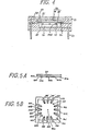
- Figure 4 shows a cross-sectional view of an improved ultra-high speed semiconductor IC device according to a first embodiment of the invention.
- An IC chip 22 is mounted in the cavity 50 of a package 21 by means of a low melting point metal sheet 60.
- Each of the pads 25 on the chip 22 is connected by a signal line 29 to respective outer lead 23 through an inner lead terminal 24 of the package 21.
- the chip 22 has a size of for example approximately 4 mm square, and is connected to the ground through the low melting point metal sheet 60 and an outer lead (not shown).
- the package 21 is converted by a cover plate 27 which is sealed hermetically to the package by a seal 70.
- the signal lines 29 are formed on a wiring board 26 which comprises a sapphire plate 28 and is arranged over the chip 22.
- the spacing between the bottom of the wiring board 26 having the signal lines 29 and the surface of the chip 22 has a value for example comprised between 30 pm and 50 pm. The spacing is a critical factor and must be uniform in order to keep constant the characteristic impedance of the transmission lines and to reduce the reflection of signal.
- the pads 25 are connected to projection leads of the signal lines which are made of gold.
- the bonding connection is realized by a known process, such as for example ball bonding or flip tip bonding.
- the processes and technology used for assembling the constitutive parts of the device of figure 4 are processes and technology conventionally used in the making of semiconductor IC device, such as bonding, metal sputtering, mounting technology, etc...Therefore, the detailed description of such processes and technology will be omitted in the following disclosure for sake of simplicity.
- the board 26 is made of a sapphire plate 28, for example, and the signal lines 20a to 20b are patterned by metallic conductors formed on the bottom of the sapphire plate 28.
- the conductors are, for example, made of gold, silver or copper.
- the conductors 20a, 20b,..., 201 are shielded by a grounded conductor 21a providing a coplane guide structure.
- Conductor 2la is grounded through a projection lead 21ab .
- the wiring board 26 has a structure showing a significant difference compared to the structure of prior art wiring boards.
- projection leads 20ab, 20bb, ..., 201b On the tips of the signal lines 20a, 20b,..., 201 are provided projection leads 20ab, 20bb, ..., 201b and, at the other ends of the signal lines are provided signal line terminals 20aa, 20ba,..., 201a.
- the projection leads 20ab to 201b are bonded to respective pads 25 and the signal line terminals 20aa to 201a are bonded to respective inner lead terminals 24 when the wiring board 26 is placed in position.
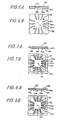
- FIGS 6A and 6B show another embodiment of a wiring board 26 with transmission lines in the form of strip lines.
- Lines 19a similar to the lines 20a to 201 of the embodiment of figures 5A, 5B are formed on the lower surface of the plate 28.
- Each line 19a has a projection lead 19ab, at one end and line terminal 19aa at the other end.
- a conductor 19c is formed on the upper surface of the plate 28 and is grounded by means of a projection lead 19bb extending through the plate 28.
- the plate 28 with the conductive surfaces formed on its lower and upper sides constitutes a strip line.
- a strip line commonly known as a wave guide
- the optimum value of the impedance of a strip line is defined from the dielectric constant of the insulator, the thickness of the insulator and the width of the strip line.
- the thickness of the sapphire plate 28 is chosen approximately 0.1 mm and the width of the strip line is selected to be 0.09 mm. So, the signals applied to the projection lead 19ab, are transferred to the signal line terminals 19aa through the signal lines 19a without transmission loss.
- FIG. 7A Another embodiment of the wiring board is illustrated by figures 7A and 7B. This embodiment only differs from the one of figures 5A, 5B by the provision of an impedance matching resistor 20d connected between the line 20a and the grounded conductor 21a.
- the impedance matching between package leads is also important to the reflection of the signal through the signal lines. With any output devices the power output varies as the load impedance varies.
- the output impedance is matched to the lead by the matching resistor 20d, to be for example equal to 50 ohms.
- the signal applied to the projection lead 20ab is transferred to the signal terminal 20aa through the line 20a without transmission loss.
- FIGS 8A and 8B Still another embodiment of the wiring board is illustrated by figures 8A and 8B. This embodiment differs from the one of figures 5A and 5B in that the wiring board is provided with a circuit element 20e for wave reforming.
- the wave reforming element 20e is mounted on the upper surface of the sapphire plate 28 and is connected in series with the signal line 20a, through the plate 28.
- Semiconductor devices intended for operation at ultra-high frequency may need reforming circuits such as 20e.
- the wave reforming circuit 20e in the form of an IC, is designed to compensate for the transmission loss due to the non-linear distorsion.
- the reforming IC 20e can be stacked to offer an increased or decreased impedance,an increased output, etc...
- a desired characteristic being the direct proportionality between the input signal wave form and that of the output, the use of wiring boards having wave reforming circuits makes it possible to reform the signals received from the projection leads 20ab and reduce the distorsion.
- through-holes 42 are formed through the plate 48 to see positioning marks + on the chip in order to ensure a proper positioning of the wiring board over the chip.
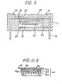
- FIGS 9 to lOD illustrate another embodiment of a device according to the invention having a multi-layered wiring board. Same or like reference numerals denote same or like parts in these figures.
- the wiring board 38 of figures 9 and lOA has a multi-layered structure.
- the use of a multi-layered wiring board makes it possible to simplify the wiring of the chip as the integration scale of the IC device increases, because it is then possible to reduce the connecting area between circuit elements on the chip.
- the multi-layered wiring board 38 is composed of a plurality of insulating plates 38a, 38b and 38c in the form of sapphire plates, for example. Though a three-layer wiring board is illustrated, it will be obvious that the number of layers can be chosen different from three.
- Each of the sapphire plates 38a, 38b, 38c has a patterned metallic conductor plane film made of gold, silver or copper, for example.
- the signal lines 40g 2 and the grounding conductors 4lbb are formed respectively on the sapphire plates 38a, 38b and 38c.
- the patterned sapphire plates 38a, 38b and 38c are stacked up and fused to form the multi-layered wiring board 38.
- the stacked board 38 includes a signal line terminal 40 and projection leads 43a, 43b,...,43g through holes connection leads 44a, 44b.
- Figure 10B shows schematically a plan view of the upper surface of the upper wiring board 38a.
- the patterned metallic films on the wiring board 38a are used for the signal lines 40a, 40b,..., 401 having respective signal line terminal leads 40aa, 40ba,...401a and for the grounded metallic conductor 41a.
- Each of the signal line terminal leads 40aa, 40ba,...,401a projects out from the plate 38a for connection to a respective inner lead terminal 34 of the package 31 (figure 9).
- the inner lead terminals 34 are connected to the outer leads 33.
- Dot lines 40a 2 , 40g 2 and 40d 2 , 40j 2 designate the signal lines which are respectively fabricated on the plate 38b and the plate 38c shown in figure 10 and figure 10D.
- the wiring plate 38a also includes through-holes 42a, and 42a 2 in order to see positioning marks (+) on the chip.
- Figure lOC illustrates schematically a plan view of the wiring pattern on the intermediary wiring sapphire plate 38b.
- the metallic pattern in this example includes a grounded metallic conductor 41b and strip signal lines 40a 2 and 40g 2 .
- a projection lead connecting hole, respectively 40ab and 40gb is formed at one end of each of the signal lines 40a 2 and 40g 2 .
- the plate 38b further includes through-holes 40bb, 40cb,...,401b to enable interconnection between the upper plate 38a and the lower plate 38c by through-hole connection. Additional through-holes 42b, and 42b 2 are provided in order to see the positioning marks on the chip.
- Figure 10D illustrates schematically a plan view of the metallic pattern on the lower wiring plate 38c.
- the pattern and material of the plate 38c are similarto the ones of the plate 38b shown in figure 10C.
- the matallic pattern includes strip lines 40d 2 and 40j 2 and, a grounded conductor 41c.
- Projection lead connecting holes 40db and 40jb are formed at respective ends of the signal lines 40d2 and 40 j 2 .
- the plate 38c also includes projection lead connecting holes 40ab, 40bb,... 401b and through-holes 42c 1 and 42c 2 for seeing the positioning marks (+) on the chip.
- Conductors 41a, 41b and 41c are connected to the ground by means of through-hole connection 4lbb (figures lOA to 10D).
- the plates 38a, 38b and 38c are assembled together with the through-holes 42a 1 , 42b 1 and 42 cl aligned, as well as the through-holes 42a2, 42b 2 and 42c 2 .
- the multi-layered wiring board 38 is positioned over the chip to align these two series of through-holes with respective positioning marks (+) 42d 1 and 42d 2 (shown in figure 10D only) provided on the chip.
- connection from the upper wiring plate 38a to the lower wiring plate is formed by through-hole connection.
- the signal line 40a provided on the upper wiring plate 38a is connected to the signal line 40a 2 on the intermediary wiring plate 38b by means of the projection lead 44a (figure lOA) through the hole connection 40bb.
- the signal line 40a 2 is connected to the projection lead 44b through the projection lead hole 40ab.
- the projection lead 43g (shown in figure lOA) is connected to a respective bonding pad of the chip.
- the connections between the sapphire plate 38c and the bonding pads are accomplished by means of the projecting leads 43a, 43b,..., 43g, through the projection lead holes 40ab, 40hb, 40jb, 40kb, 40db, 40gb and 40bb.
- the wirings between the signal lines can cross each other and, in particular, the output pads 35 can be set in any position on the chip 32. This enables to reduce the connecting area between circuit elements on the chip, so that the integration scale of the semiconductor IC device can be increased.
- the invention allows the design of a wiring board having an optimum performance for ultra-high speed operation for high density integrated circuit devices. For example, using a multi-layered wiring board such as described hereinbefore, an operation speed of approximately 100 Gbit/s has been attained.
Abstract
Description
- This invention relates to a semiconductor integrated circuit device, and, more particularly, to a layout and connecting structure between inner lead terminals of a package and bonding pads on a chip for an ultra-high speed semiconductor integrated circuit device.
- As the scale of integration of semiconductor devices increases, the improvement of efficiency and processing speed of the devices becomes consequently more and more important.In the field of ultra-high speed semiconductor IC devices, gallium arsenide (GaAs) is widely used since its carrier mobility is greater than that of silicon. Operating GaAs semiconductor devices at more than 10 gigabits per second (Gbit/s) without difficulty has been reported, but it is still difficult to operate GaAs semiconductor devices at a speed as high as 100 Gbit/s. Also, as the scale of integration increases, the making of interconnections between elements of the device becomes complicated and constitutes a serious problem to resolve for ultra-high speed IC devices.
- Figures 1 and 2 are schematical cross-sectional views of prior art structures of semiconductor IC devices such as GaAs IC devices. In these figures,
reference numerals 1 and 11 designate packages, 2 and 12 are semiconductor chips mounted in thepackages packages 1 and 11. The GaAssubstrate chip cavity 50 of thepackage 1, 11 and is bonded to the ceramic package by means of a low melting point metal sheet 60. The chip size is for example approximately 4 mm square. Ahermetic seal 70 is provided for hermetically sealing thecover plate package 1, 11. - In the embodiment of figure 1, inner leads 6 are provided for connecting the
bonding pads 5 to respectiveouter leads 3 through the inner lead terminals 4. - In the embodiment of figure 2, a
wiring board 16 having a printed wiring circuit is provided for connecting thebonding pads 15 to respectiveouter leads 13 through theinner lead terminals 14. - Figures 3A and 3B are respectively cross-sectional and bottom plan views of the
wiring board 16 of figure 2. Thiswiring board 16 is arranged above thechip 12 and includes aninsulating plate 18, a positioning mark 18a andsignal lines inner lead terminal 14 and a projection lead 19ab connected to arespective bonding pad 15. - The increase of the integration scale of the semiconductor device has made the realization of inner leads 6 between the chip and the outer leads 3 more and more complicated.
- By using a wiring board such as 16, the wiring of the IC device is simplified. In most prior art devices, multi-lead packages having wiring boards as shown in figure 2 are used.
- A study of currently available IC packages in order to develop their performance for operating at ultra-high speed has shown when the operation speed is increased up to ultra-high speeds of approximately 100 Gbit/s, devices having a conventional structure show disadvantages such as large reflection and attenuation of the signal on its transmission lines in the package.
- It is therefore an object of the invention to provide an improved ultra-high speed semiconductor device having a wiring board structure enabling to improve the operation speed while reducing the reflection and transmission line loss at ultra-high operation speed.
- The foregoing object is accomplished according to the invention by providing a wiring board comprising a transmission ?.ine fabricated on an insulating plate, said transmission line having predetermined transmission characteristics by arranging a signal line conductor and a ground conductor plane with a predetermined spacing therebetween, and said signal line conductor connecting an output terminal of the semiconductor chip to a respective outer lead.
- The transmission line is in the form of a coplanar guide or a strip line.
- A multi-layer wiring board can be used with through-hole connections. With such a configuration, the output pads of the chip can be positioned at any point on the chip.
- By applying the high frequency technology of coplanar guides or strip lines together with impedance matching resistors and wave reforming circuit elements, it is possible to design a wiring board, in particular a multi-layer wiring board, enabling to reduce the reflection and attenuation of the signal resulting from the use of prior art inner lead structures, and which has then an optimum performance for ultra-high speed operation.
- These and other features of the invention will become more apparent from the following description taken in connection with the accompanying drawings wherein :
- - Figure 1 illustrates schematically a cross-sectional view of a structure of a prior art semiconductor IC device;
- - Figure 2 illustrates schematically a cross-sectional view of a structure of a prior art multi-lead semiconductor IC device,
- - Figure 3A illustrates schematically a cross-sectional view of the wiring board of the structure shown in Figure 2;
- - Figure 3B illustrates schematically a bottom plan view of the wiring board of Figure 3A;
- - Figure 4 illustrates schematically a cross-sectional view of an improved ultra-high speed semiconductor 1C device according to a first embodiment of the present invention;
- - Figure 5A illustrates schematically a cross-sectional view of the wiring board of the device of Figure 4;
- - Figure 5B illustrates schematically the bottom plan view of the wiring board of Figure 5A;
- - Figure 6A illustrates schematically a cross-sectional view of another structure of the wiring board of the device of Figure 4;
- - Figure 6B illustratesschematically the bottom plan view of the wiring board of Figure 6A;
- - Figure 7A illustrates schematically a cross-sectional view of still another structure of the wiring board of the device of Figure 4 ;
- - Figure 7B illustrates schematically the bottom plan view of the wiring board of Figure 7A;
- - Figure 8A illustrates schematically a cross-sectional view of a further structure of the wiring board of the device of Figure 4;
- - Figure 8B illustrates schematically a bottom plan view of the wiring board of Figure 8A;
- - Figure 9 illustrates schematically a cross-sectional view of an improved ultra-high speed semiconductor IC device according to a second embodiment of the present invention;
- - Figure lOA illustrates schematically a cross-sectional view of a structure of the multi-layered wiring board of the device of Figure 9;
- - Figure lOB illustrates schematically the plan view of an upper part of the wiring board of Figure lOA;
- - Figure 10C illustrates schematically a plan view of an intermediary part of the wiring board of Figure lOA; and
- - Figure 10D illustrates schematically a plan view of a bottom part of the wiring board of Figure 10A.
- Same or like reference numerals denote the same or like parts through the drawings.
- Figure 4 shows a cross-sectional view of an improved ultra-high speed semiconductor IC device according to a first embodiment of the invention.
- An
IC chip 22 is mounted in thecavity 50 of apackage 21 by means of a low meltingpoint metal sheet 60. Each of thepads 25 on thechip 22 is connected by asignal line 29 to respectiveouter lead 23 through aninner lead terminal 24 of thepackage 21. Thechip 22 has a size of for example approximately 4 mm square, and is connected to the ground through the low meltingpoint metal sheet 60 and an outer lead (not shown). Thepackage 21 is converted by acover plate 27 which is sealed hermetically to the package by aseal 70. - The
signal lines 29 are formed on awiring board 26 which comprises asapphire plate 28 and is arranged over thechip 22. The spacing between the bottom of thewiring board 26 having thesignal lines 29 and the surface of thechip 22 has a value for example comprised between 30 pm and 50 pm. The spacing is a critical factor and must be uniform in order to keep constant the characteristic impedance of the transmission lines and to reduce the reflection of signal. Thepads 25 are connected to projection leads of the signal lines which are made of gold. The bonding connection is realized by a known process, such as for example ball bonding or flip tip bonding. - The processes and technology used for assembling the constitutive parts of the device of figure 4 are processes and technology conventionally used in the making of semiconductor IC device, such as bonding, metal sputtering, mounting technology, etc...Therefore, the detailed description of such processes and technology will be omitted in the following disclosure for sake of simplicity.
- A detailed structure of an embodiment of the
wiring board 26 having signal lines in the form of coplanar guides will now be described with respect to figures 5A and 5B. Theboard 26 is made of asapphire plate 28, for example, and the signal lines 20a to 20b are patterned by metallic conductors formed on the bottom of thesapphire plate 28. The conductors are, for example, made of gold, silver or copper. As shown in figure 5B, theconductors 20a, 20b,..., 201 are shielded by agrounded conductor 21a providing a coplane guide structure. Conductor 2la is grounded through a projection lead 21ab . - Thus, the
wiring board 26 has a structure showing a significant difference compared to the structure of prior art wiring boards. By adapting the coplanar guide structure to the wiring board, it is possible to reduce the reflection of signal and the attenuation of the transmission lines for ultra-high speed 1C device, and thus enable the signals on thepads 25 to be transferred to theouter leads 23 through the transmission lines without substantial transmission loss. - On the tips of the
signal lines 20a, 20b,..., 201 are provided projection leads 20ab, 20bb, ..., 201b and, at the other ends of the signal lines are provided signal line terminals 20aa, 20ba,..., 201a. The projection leads 20ab to 201b are bonded torespective pads 25 and the signal line terminals 20aa to 201a are bonded to respectiveinner lead terminals 24 when thewiring board 26 is placed in position. - Figures 6A and 6B show another embodiment of a
wiring board 26 with transmission lines in the form of strip lines.Lines 19a similar to the lines 20a to 201 of the embodiment of figures 5A, 5B are formed on the lower surface of theplate 28. Eachline 19a has a projection lead 19ab, at one end and line terminal 19aa at the other end. A conductor 19c is formed on the upper surface of theplate 28 and is grounded by means of a projection lead 19bb extending through theplate 28. - The
plate 28 with the conductive surfaces formed on its lower and upper sides constitutes a strip line. For a further description of a strip line, commonly known as a wave guide, reference is made to a report entitled "Microwave Integrated Circuits" by Gupta K.C. and Singh A in John Wiley & Sons (1974) which disclosed a strip line on the same principle as the one hereinabove mentioned. According to this report, the optimum value of the impedance of a strip line is defined from the dielectric constant of the insulator, the thickness of the insulator and the width of the strip line. Therefore, in order to obtain an optimum value of the impedance Z0 equal , for example, to 50 ohms, the condition W / h = 0.9 must be met, where W is the width of strip line and h is the thickness of the sapphire plate (specific inductive capacity of sapphire E is 10.55). As a result, the thickness of thesapphire plate 28 is chosen approximately 0.1 mm and the width of the strip line is selected to be 0.09 mm. So, the signals applied to the projection lead 19ab, are transferred to the signal line terminals 19aa through thesignal lines 19a without transmission loss. - Another embodiment of the wiring board is illustrated by figures 7A and 7B. This embodiment only differs from the one of figures 5A, 5B by the provision of an
impedance matching resistor 20d connected between the line 20a and the groundedconductor 21a. - All semiconductor devices and particularly those intended for operation at high frequency, require a suitable impedance matching to the output circuits in order to provide enough output power. The impedance matching between package leads is also important to the reflection of the signal through the signal lines. With any output devices the power output varies as the load impedance varies. By using a wiring board with a signal line 20a loaded or an
impedance matching resistor 20d in parallel, the output impedance is matched to the lead by the matchingresistor 20d, to be for example equal to 50 ohms. Thus, the signal applied to the projection lead 20ab is transferred to the signal terminal 20aa through the line 20a without transmission loss. - Still another embodiment of the wiring board is illustrated by figures 8A and 8B. This embodiment differs from the one of figures 5A and 5B in that the wiring board is provided with a
circuit element 20e for wave reforming. - The
wave reforming element 20e is mounted on the upper surface of thesapphire plate 28 and is connected in series with the signal line 20a, through theplate 28. Semiconductor devices intended for operation at ultra-high frequency may need reforming circuits such as 20e. In the case, for example, of non-linear distorsion of the signal on the transmission line, thewave reforming circuit 20e, in the form of an IC, is designed to compensate for the transmission loss due to the non-linear distorsion. Also, as in the case of the above-mentioned resistor, or as capacitors or other components, the reformingIC 20e can be stacked to offer an increased or decreased impedance,an increased output, etc... A desired characteristic being the direct proportionality between the input signal wave form and that of the output, the use of wiring boards having wave reforming circuits makes it possible to reform the signals received from the projection leads 20ab and reduce the distorsion. - In all the above described embodiments of the wiring board, through-
holes 42 are formed through the plate 48 to see positioning marks + on the chip in order to ensure a proper positioning of the wiring board over the chip. - Figures 9 to lOD illustrate another embodiment of a device according to the invention having a multi-layered wiring board. Same or like reference numerals denote same or like parts in these figures.
- By constrast with the hereinabove described wiring boards, the
wiring board 38 of figures 9 and lOA has a multi-layered structure. The use of a multi-layered wiring boardmakes it possible to simplify the wiring of the chip as the integration scale of the IC device increases, because it is then possible to reduce the connecting area between circuit elements on the chip. - As shown in figure 10A, the
multi-layered wiring board 38 is composed of a plurality of insulatingplates sapphire plates sapphire plates sapphire plates multi-layered wiring board 38. The stackedboard 38 includes asignal line terminal 40 and projection leads 43a, 43b,...,43g through holes connection leads 44a, 44b. - Figure 10B shows schematically a plan view of the upper surface of the
upper wiring board 38a. The patterned metallic films on thewiring board 38a are used for the signal lines 40a, 40b,..., 401 having respective signal line terminal leads 40aa, 40ba,...401a and for the grounded metallic conductor 41a. Each of the signal line terminal leads 40aa, 40ba,...,401a projects out from theplate 38a for connection to a respectiveinner lead terminal 34 of the package 31 (figure 9). Theinner lead terminals 34 are connected to the outer leads 33. Dot lines 40a2, 40g2 and 40d2, 40j2 designate the signal lines which are respectively fabricated on theplate 38b and the plate 38c shown in figure 10 and figure 10D. Thewiring plate 38a also includes through-holes 42a, and 42a2 in order to see positioning marks (+) on the chip. - Figure lOC illustrates schematically a plan view of the wiring pattern on the intermediary
wiring sapphire plate 38b. The metallic pattern in this example includes a grounded metallic conductor 41b and strip signal lines 40a2 and 40g2. A projection lead connecting hole, respectively 40ab and 40gb is formed at one end of each of the signal lines 40a2 and 40g2. Moreover, theplate 38b further includes through-holes 40bb, 40cb,...,401b to enable interconnection between theupper plate 38a and the lower plate 38c by through-hole connection. Additional through-holes 42b, and 42b2 are provided in order to see the positioning marks on the chip. - Figure 10D illustrates schematically a plan view of the metallic pattern on the lower wiring plate 38c. The pattern and material of the plate 38c are similarto the ones of the
plate 38b shown in figure 10C. The matallic pattern includes strip lines 40d2 and 40j2 and, a grounded conductor 41c. Projection lead connecting holes 40db and 40jb are formed at respective ends of the signal lines 40d2 and 40j2. The plate 38c also includes projection lead connecting holes 40ab, 40bb,... 401b and through-holes 42c1 and 42c2 for seeing the positioning marks (+) on the chip. - Conductors 41a, 41b and 41c are connected to the ground by means of through-hole connection 4lbb (figures lOA to 10D).
- The
plates holes 42a1, 42b1 and 42cl aligned, as well as the through-holes 42a2, 42b2 and 42c2. Themulti-layered wiring board 38 is positioned over the chip to align these two series of through-holes with respective positioning marks (+) 42d1 and 42d2 (shown in figure 10D only) provided on the chip. - The connection from the
upper wiring plate 38a to the lower wiring plate is formed by through-hole connection. For example, the signal line 40a provided on theupper wiring plate 38a is connected to the signal line 40a2 on theintermediary wiring plate 38b by means of the projection lead 44a (figure lOA) through the hole connection 40bb. Similarly, the signal line 40a2 is connected to theprojection lead 44b through the projection lead hole 40ab. Finally, theprojection lead 43g (shown in figure lOA) is connected to a respective bonding pad of the chip. - Similarly, the connections between the sapphire plate 38c and the bonding pads are accomplished by means of the projecting leads 43a, 43b,..., 43g, through the projection lead holes 40ab, 40hb, 40jb, 40kb, 40db, 40gb and 40bb. Furthermore, it is possible to have the wirings between the signal lines to cross each other and, in particular, the
output pads 35 can be set in any position on thechip 32. This enables to reduce the connecting area between circuit elements on the chip, so that the integration scale of the semiconductor IC device can be increased. As a result, the invention allows the design of a wiring board having an optimum performance for ultra-high speed operation for high density integrated circuit devices. For example, using a multi-layered wiring board such as described hereinbefore, an operation speed of approximately 100 Gbit/s has been attained. - Although only ultra-high speed GaAs semiconductor devices have been mentioned, it is obvious that the invention can be applied to other semiconductor devices.
Claims (7)
Applications Claiming Priority (4)
| Application Number | Priority Date | Filing Date | Title |
|---|---|---|---|
| JP243410/83 | 1983-12-23 | ||
| JP58243410A JPS60136232A (en) | 1983-12-23 | 1983-12-23 | Semiconductor integrated circuit device |
| JP58249336A JPS60140727A (en) | 1983-12-27 | 1983-12-27 | Semiconductor integrated circuit device |
| JP249336/83 | 1983-12-27 |
Publications (3)
| Publication Number | Publication Date |
|---|---|
| EP0148083A2 true EP0148083A2 (en) | 1985-07-10 |
| EP0148083A3 EP0148083A3 (en) | 1986-10-08 |
| EP0148083B1 EP0148083B1 (en) | 1990-05-23 |
Family
ID=26536242
Family Applications (1)
| Application Number | Title | Priority Date | Filing Date |
|---|---|---|---|
| EP84402696A Expired - Lifetime EP0148083B1 (en) | 1983-12-23 | 1984-12-21 | Ultra-high speed semiconductor integrated circuit device having a multi-layered wiring board |
Country Status (4)
| Country | Link |
|---|---|
| US (1) | US4751482A (en) |
| EP (1) | EP0148083B1 (en) |
| KR (1) | KR900001273B1 (en) |
| DE (1) | DE3482353D1 (en) |
Cited By (11)
| Publication number | Priority date | Publication date | Assignee | Title |
|---|---|---|---|---|
| EP0171232A2 (en) * | 1984-08-09 | 1986-02-12 | Minnesota Mining And Manufacturing Company | Area-bonding tape |
| WO1987004010A1 (en) * | 1985-12-20 | 1987-07-02 | Hughes Aircraft Company | Chip interface mesa |
| EP0239494A1 (en) * | 1986-03-28 | 1987-09-30 | Bull S.A. | Integrated circuit housing |
| EP0246458A2 (en) * | 1986-05-19 | 1987-11-25 | International Business Machines Corporation | Module for packaging semiconductor integrated circuit chips on a base substrate |
| EP0272187A2 (en) * | 1986-12-17 | 1988-06-22 | Fairchild Semiconductor Corporation | Plastic package for high frequency semiconductor devices |
| EP0335740A2 (en) * | 1988-03-31 | 1989-10-04 | Kabushiki Kaisha Toshiba | IC packing device with impedance adjusting insulative layer |
| EP0344702A2 (en) * | 1988-05-30 | 1989-12-06 | Canon Kabushiki Kaisha | Electric circuit apparatus |
| EP0491161A1 (en) * | 1990-11-16 | 1992-06-24 | Ball Corporation | Interconnect package for circuitry components |
| US5162896A (en) * | 1987-06-02 | 1992-11-10 | Kabushiki Kaisha Toshiba | IC package for high-speed semiconductor integrated circuit device |
| GB2264389A (en) * | 1991-12-26 | 1993-08-25 | Fuji Electric Co Ltd | Connections for power semiconductor devices |
| DE4223371A1 (en) * | 1992-07-16 | 1994-01-20 | Thomson Brandt Gmbh | Electronic component mounting method for circuit board assembly - with openings in cover layer overlapping each component receiving conductive paste providing required electrical connections |
Families Citing this family (53)
| Publication number | Priority date | Publication date | Assignee | Title |
|---|---|---|---|---|
| US5917707A (en) | 1993-11-16 | 1999-06-29 | Formfactor, Inc. | Flexible contact structure with an electrically conductive shell |
| JPS63258046A (en) * | 1987-04-15 | 1988-10-25 | Toshiba Corp | Semiconductor integrated circuit device |
| US5334962A (en) * | 1987-09-18 | 1994-08-02 | Q-Dot Inc. | High-speed data supply pathway systems |
| JP2507476B2 (en) * | 1987-09-28 | 1996-06-12 | 株式会社東芝 | Semiconductor integrated circuit device |
| US5162822A (en) * | 1988-10-31 | 1992-11-10 | Hitachi, Ltd. | Saw filter chip mounted on a substrate with shielded conductors on opposite surfaces |
| US5136271A (en) * | 1989-01-09 | 1992-08-04 | Mitsubishi Denki Kabushiki Kaisha | Microwave integrated circuit mountings |
| US5135890A (en) * | 1989-06-16 | 1992-08-04 | General Electric Company | Method of forming a hermetic package having a lead extending through an aperture in the package lid and packaged semiconductor chip |
| US5103290A (en) * | 1989-06-16 | 1992-04-07 | General Electric Company | Hermetic package having a lead extending through an aperture in the package lid and packaged semiconductor chip |
| US5209390A (en) * | 1989-07-03 | 1993-05-11 | General Electric Company | Hermetic package and packaged semiconductor chip having closely spaced leads extending through the package lid |
| US5166773A (en) * | 1989-07-03 | 1992-11-24 | General Electric Company | Hermetic package and packaged semiconductor chip having closely spaced leads extending through the package lid |
| US5006820A (en) * | 1989-07-03 | 1991-04-09 | Motorola, Inc. | Low reflection input configuration for integrated circuit packages |
| GB8918482D0 (en) * | 1989-08-14 | 1989-09-20 | Inmos Ltd | Packaging semiconductor chips |
| WO1991007777A1 (en) * | 1989-11-22 | 1991-05-30 | Tactical Fabs, Inc. | High density multichip package |
| US5182632A (en) * | 1989-11-22 | 1993-01-26 | Tactical Fabs, Inc. | High density multichip package with interconnect structure and heatsink |
| US5148266A (en) * | 1990-09-24 | 1992-09-15 | Ist Associates, Inc. | Semiconductor chip assemblies having interposer and flexible lead |
| US5258330A (en) * | 1990-09-24 | 1993-11-02 | Tessera, Inc. | Semiconductor chip assemblies with fan-in leads |
| US5148265A (en) * | 1990-09-24 | 1992-09-15 | Ist Associates, Inc. | Semiconductor chip assemblies with fan-in leads |
| US5679977A (en) * | 1990-09-24 | 1997-10-21 | Tessera, Inc. | Semiconductor chip assemblies, methods of making same and components for same |
| US20010030370A1 (en) * | 1990-09-24 | 2001-10-18 | Khandros Igor Y. | Microelectronic assembly having encapsulated wire bonding leads |
| US7198969B1 (en) * | 1990-09-24 | 2007-04-03 | Tessera, Inc. | Semiconductor chip assemblies, methods of making same and components for same |
| JP3011510B2 (en) * | 1990-12-20 | 2000-02-21 | 株式会社東芝 | Semiconductor device having interconnected circuit board and method of manufacturing the same |
| US5107328A (en) * | 1991-02-13 | 1992-04-21 | Micron Technology, Inc. | Packaging means for a semiconductor die having particular shelf structure |
| US5155067A (en) * | 1991-03-26 | 1992-10-13 | Micron Technology, Inc. | Packaging for a semiconductor die |
| US5311058A (en) * | 1991-11-29 | 1994-05-10 | Trw Inc. | Integrated circuit power distribution system |
| EP0547807A3 (en) * | 1991-12-16 | 1993-09-22 | General Electric Company | Packaged electronic system |
| JP3267409B2 (en) * | 1992-11-24 | 2002-03-18 | 株式会社日立製作所 | Semiconductor integrated circuit device |
| JPH08504541A (en) * | 1992-12-15 | 1996-05-14 | イー・アイ・デユポン・ドウ・ヌムール・アンド・カンパニー | Electrical interconnection structure |
| JPH06268020A (en) * | 1993-03-10 | 1994-09-22 | Sumitomo Electric Ind Ltd | Semiconductor device |
| US5338970A (en) * | 1993-03-24 | 1994-08-16 | Intergraph Corporation | Multi-layered integrated circuit package with improved high frequency performance |
| US5820014A (en) | 1993-11-16 | 1998-10-13 | Form Factor, Inc. | Solder preforms |
| US5566448A (en) * | 1995-06-06 | 1996-10-22 | International Business Machines Corporation | Method of construction for multi-tiered cavities used in laminate carriers |
| US5777379A (en) | 1995-08-18 | 1998-07-07 | Tessera, Inc. | Semiconductor assemblies with reinforced peripheral regions |
| US8033838B2 (en) | 1996-02-21 | 2011-10-11 | Formfactor, Inc. | Microelectronic contact structure |
| US5994152A (en) | 1996-02-21 | 1999-11-30 | Formfactor, Inc. | Fabricating interconnects and tips using sacrificial substrates |
| KR100186329B1 (en) * | 1996-06-14 | 1999-03-20 | 문정환 | Semiconductor package for charge coupled device |
| US5757041A (en) | 1996-09-11 | 1998-05-26 | Northrop Grumman Corporation | Adaptable MMIC array |
| US5937276A (en) * | 1996-12-13 | 1999-08-10 | Tessera, Inc. | Bonding lead structure with enhanced encapsulation |
| DE19734032C1 (en) * | 1997-08-06 | 1998-12-17 | Siemens Ag | Electronic control device with manufacturing procedure e.g. for installing in oil-sump of automobile automatic transmission |
| US6008533A (en) * | 1997-12-08 | 1999-12-28 | Micron Technology, Inc. | Controlling impedances of an integrated circuit |
| JP2000031274A (en) * | 1998-07-14 | 2000-01-28 | Matsushita Electric Ind Co Ltd | Semiconductor device |
| US6181004B1 (en) * | 1999-01-22 | 2001-01-30 | Jerry D. Koontz | Digital signal processing assembly and test method |
| DE19907949C2 (en) * | 1999-02-24 | 2002-11-07 | Siemens Ag | Control device for a motor vehicle |
| SE514426C2 (en) * | 1999-06-17 | 2001-02-19 | Ericsson Telefon Ab L M | Device for chip mounting in cavity in multilayer PCBs |
| AU2001227912A1 (en) * | 2000-01-13 | 2001-07-24 | Alpha Industries, Inc. | Microwave ic package with dual mode wave guide |
| US6388886B1 (en) * | 2000-05-08 | 2002-05-14 | Mitsubishi Denki Kabushiki Kaisha | Semiconductor memory module and module system |
| US6608390B2 (en) | 2001-11-13 | 2003-08-19 | Kulicke & Soffa Investments, Inc. | Wirebonded semiconductor package structure and method of manufacture |
| US6803252B2 (en) | 2001-11-21 | 2004-10-12 | Sierra Monolithics, Inc. | Single and multiple layer packaging of high-speed/high-density ICs |
| US20030095014A1 (en) * | 2001-11-21 | 2003-05-22 | Lao Binneg Y. | Connection package for high-speed integrated circuit |
| JP2003258178A (en) * | 2002-02-27 | 2003-09-12 | Sanyo Electric Co Ltd | Semiconductor device |
| JP2003258179A (en) * | 2002-02-28 | 2003-09-12 | Sanyo Electric Co Ltd | Semiconductor device and manufacturing method therefor |
| US20040105244A1 (en) * | 2002-08-06 | 2004-06-03 | Ilyas Mohammed | Lead assemblies with offset portions and microelectronic assemblies with leads having offset portions |
| CN1315186C (en) * | 2004-05-01 | 2007-05-09 | 江苏长电科技股份有限公司 | Mini flipchip transistor and method for manufacturing same |
| US10390455B2 (en) * | 2017-03-27 | 2019-08-20 | Raytheon Company | Thermal isolation of cryo-cooled components from circuit boards or other structures |
Citations (4)
| Publication number | Priority date | Publication date | Assignee | Title |
|---|---|---|---|---|
| FR1534329A (en) * | 1966-08-16 | 1968-07-26 | Signetics Corp | Integrated circuit assembly process |
| US4096348A (en) * | 1975-06-04 | 1978-06-20 | Raytheon Company | Integrated test and assembly device |
| EP0101335A1 (en) * | 1982-06-29 | 1984-02-22 | Thomson-Csf | Encapsulating microhousing for very high frequency logic integrated circuits |
| FR2535110A1 (en) * | 1982-10-20 | 1984-04-27 | Radiotechnique Compelec | Method of encapsulating a semiconductor component in an electronic circuit made on a substrate and application to high-speed integrated circuits. |
Family Cites Families (20)
| Publication number | Priority date | Publication date | Assignee | Title |
|---|---|---|---|---|
| NL275288A (en) * | 1961-02-28 | |||
| DE1244257B (en) * | 1961-05-25 | 1967-07-13 | Emi Ltd | Circuit arrangement for the reaction-free coupling of two voltages to form a total voltage with three strip conductors opposite a grounded common conductor |
| US3218584A (en) * | 1964-01-02 | 1965-11-16 | Sanders Associates Inc | Strip line connection |
| US3303439A (en) * | 1965-06-14 | 1967-02-07 | Western Electric Co | Strip transmission line interboard connection |
| US3614832A (en) * | 1966-03-09 | 1971-10-26 | Ibm | Decal connectors and methods of forming decal connections to solid state devices |
| US3417294A (en) * | 1966-12-19 | 1968-12-17 | Emc Technology Inc | Mounting circuit elements in printed circuit boards |
| JPS4947713B1 (en) * | 1970-04-27 | 1974-12-17 | ||
| DE2346924A1 (en) * | 1973-09-18 | 1975-03-27 | Siemens Ag | Wideband termination resistor for micro strip-line - has ohmic resistor in substrate with thin wire connection to line |
| US3895435A (en) * | 1974-01-23 | 1975-07-22 | Raytheon Co | Method for electrically interconnecting multilevel stripline circuitry |
| US3886505A (en) * | 1974-04-29 | 1975-05-27 | Rca Corp | Semiconductor package having means to tune out output capacitance |
| US3959874A (en) * | 1974-12-20 | 1976-06-01 | Western Electric Company, Inc. | Method of forming an integrated circuit assembly |
| JPS54131851A (en) * | 1978-04-04 | 1979-10-13 | Mitsubishi Electric Corp | Multi-layer transmission line assembly |
| DE2838317C2 (en) * | 1978-09-01 | 1984-03-29 | Siemens AG, 1000 Berlin und 8000 München | Directional coupler |
| US4276558A (en) * | 1979-06-15 | 1981-06-30 | Ford Aerospace & Communications Corp. | Hermetically sealed active microwave integrated circuit |
| SE426894B (en) * | 1981-06-30 | 1983-02-14 | Ericsson Telefon Ab L M | IMPEDANCY COAXIAL TRANSFER FOR MICROVAG SIGNALS |
| EP0070104A3 (en) * | 1981-07-10 | 1985-05-15 | The Secretary of State for Defence in Her Britannic Majesty's Government of the United Kingdom of Great Britain and | Circuit matching elements |
| JPS5931042A (en) * | 1982-08-12 | 1984-02-18 | Mitsubishi Electric Corp | Semiconductor device with high frequency and output |
| US4551746A (en) * | 1982-10-05 | 1985-11-05 | Mayo Foundation | Leadless chip carrier apparatus providing an improved transmission line environment and improved heat dissipation |
| US4538170A (en) * | 1983-01-03 | 1985-08-27 | General Electric Company | Power chip package |
| US4593243A (en) * | 1984-08-29 | 1986-06-03 | Magnavox Government And Industrial Electronics Company | Coplanar and stripline probe card apparatus |
-
1984
- 1984-12-11 KR KR1019840007835A patent/KR900001273B1/en not_active IP Right Cessation
- 1984-12-21 DE DE8484402696T patent/DE3482353D1/en not_active Expired - Lifetime
- 1984-12-21 EP EP84402696A patent/EP0148083B1/en not_active Expired - Lifetime
-
1986
- 1986-10-20 US US06/920,938 patent/US4751482A/en not_active Expired - Lifetime
Patent Citations (4)
| Publication number | Priority date | Publication date | Assignee | Title |
|---|---|---|---|---|
| FR1534329A (en) * | 1966-08-16 | 1968-07-26 | Signetics Corp | Integrated circuit assembly process |
| US4096348A (en) * | 1975-06-04 | 1978-06-20 | Raytheon Company | Integrated test and assembly device |
| EP0101335A1 (en) * | 1982-06-29 | 1984-02-22 | Thomson-Csf | Encapsulating microhousing for very high frequency logic integrated circuits |
| FR2535110A1 (en) * | 1982-10-20 | 1984-04-27 | Radiotechnique Compelec | Method of encapsulating a semiconductor component in an electronic circuit made on a substrate and application to high-speed integrated circuits. |
Cited By (19)
| Publication number | Priority date | Publication date | Assignee | Title |
|---|---|---|---|---|
| EP0171232A2 (en) * | 1984-08-09 | 1986-02-12 | Minnesota Mining And Manufacturing Company | Area-bonding tape |
| EP0171232A3 (en) * | 1984-08-09 | 1987-12-02 | Minnesota Mining And Manufacturing Company | Area-bonding tape |
| WO1987004010A1 (en) * | 1985-12-20 | 1987-07-02 | Hughes Aircraft Company | Chip interface mesa |
| EP0239494A1 (en) * | 1986-03-28 | 1987-09-30 | Bull S.A. | Integrated circuit housing |
| FR2596607A1 (en) * | 1986-03-28 | 1987-10-02 | Bull Sa | METHOD FOR MOUNTING AN INTEGRATED CIRCUIT ON A CIRCUIT BOARD, INTEGRATED CIRCUIT BOX AND INTEGRATED CIRCUIT BOARD FOR IMPLEMENTING THE METHOD |
| US4812949A (en) * | 1986-03-28 | 1989-03-14 | Bull, S.A. | Method of and apparatus for mounting an IC chip |
| EP0246458A3 (en) * | 1986-05-19 | 1988-11-09 | International Business Machines Corporation | Module for packaging semiconductor integrated circuit chips on a base substrate |
| EP0246458A2 (en) * | 1986-05-19 | 1987-11-25 | International Business Machines Corporation | Module for packaging semiconductor integrated circuit chips on a base substrate |
| EP0272187A3 (en) * | 1986-12-17 | 1988-08-31 | Fairchild Semiconductor Corporation | Plastic package for high frequency semiconductor devices |
| EP0272187A2 (en) * | 1986-12-17 | 1988-06-22 | Fairchild Semiconductor Corporation | Plastic package for high frequency semiconductor devices |
| US5162896A (en) * | 1987-06-02 | 1992-11-10 | Kabushiki Kaisha Toshiba | IC package for high-speed semiconductor integrated circuit device |
| EP0335740A2 (en) * | 1988-03-31 | 1989-10-04 | Kabushiki Kaisha Toshiba | IC packing device with impedance adjusting insulative layer |
| EP0335740A3 (en) * | 1988-03-31 | 1991-05-02 | Kabushiki Kaisha Toshiba | Ic packing device with impedance adjusting insulative layer |
| EP0344702A2 (en) * | 1988-05-30 | 1989-12-06 | Canon Kabushiki Kaisha | Electric circuit apparatus |
| EP0344702B1 (en) * | 1988-05-30 | 1996-03-13 | Canon Kabushiki Kaisha | Electric circuit apparatus |
| EP0491161A1 (en) * | 1990-11-16 | 1992-06-24 | Ball Corporation | Interconnect package for circuitry components |
| GB2264389A (en) * | 1991-12-26 | 1993-08-25 | Fuji Electric Co Ltd | Connections for power semiconductor devices |
| GB2264389B (en) * | 1991-12-26 | 1995-08-30 | Fuji Electric Co Ltd | Power semiconductor device |
| DE4223371A1 (en) * | 1992-07-16 | 1994-01-20 | Thomson Brandt Gmbh | Electronic component mounting method for circuit board assembly - with openings in cover layer overlapping each component receiving conductive paste providing required electrical connections |
Also Published As
| Publication number | Publication date |
|---|---|
| EP0148083A3 (en) | 1986-10-08 |
| KR850005158A (en) | 1985-08-21 |
| KR900001273B1 (en) | 1990-03-05 |
| EP0148083B1 (en) | 1990-05-23 |
| DE3482353D1 (en) | 1990-06-28 |
| US4751482A (en) | 1988-06-14 |
Similar Documents
| Publication | Publication Date | Title |
|---|---|---|
| EP0148083B1 (en) | Ultra-high speed semiconductor integrated circuit device having a multi-layered wiring board | |
| US5014115A (en) | Coplanar waveguide semiconductor package | |
| US5006673A (en) | Fabrication of pad array carriers from a universal interconnect structure | |
| US5057805A (en) | Microwave semiconductor device | |
| US4941033A (en) | Semiconductor integrated circuit device | |
| US6184463B1 (en) | Integrated circuit package for flip chip | |
| KR100430299B1 (en) | Radio frequency circuit module on multi-layer substrate | |
| US5349317A (en) | High frequency signal transmission tape | |
| JP3461204B2 (en) | Multi-chip module | |
| US5225709A (en) | Package having a structure for stabilizing and/or impedance-matching a semiconductor IC device accommodated therein | |
| US7236373B2 (en) | Electronic device capable of preventing electromagnetic wave from being radiated | |
| EP0195520A1 (en) | Coplanar microstrap waveguide | |
| US5061990A (en) | Semiconductor device and the manufacture thereof | |
| EP0977298B1 (en) | High-frequency module | |
| JPH04137655A (en) | Ic package | |
| US5977624A (en) | Semiconductor package and assembly for fabricating the same | |
| US5426319A (en) | High-frequency semiconductor device including microstrip transmission line | |
| GB2307102A (en) | High frequency module package | |
| US6204555B1 (en) | Microwave-frequency hybrid integrated circuit | |
| GB2189084A (en) | Integrated circuit packaging | |
| EP1372215A2 (en) | Semiconductor module structure incorporating antenna | |
| US5736784A (en) | Variable-width lead interconnection structure and method | |
| JP3489926B2 (en) | High frequency circuit device | |
| JP3140385B2 (en) | High frequency semiconductor device | |
| JP2722451B2 (en) | Semiconductor device |
Legal Events
| Date | Code | Title | Description |
|---|---|---|---|
| PUAI | Public reference made under article 153(3) epc to a published international application that has entered the european phase |
Free format text: ORIGINAL CODE: 0009012 |
|
| AK | Designated contracting states |
Designated state(s): DE FR GB |
|
| PUAL | Search report despatched |
Free format text: ORIGINAL CODE: 0009013 |
|
| AK | Designated contracting states |
Kind code of ref document: A3 Designated state(s): DE FR GB |
|
| 17P | Request for examination filed |
Effective date: 19870406 |
|
| 17Q | First examination report despatched |
Effective date: 19890621 |
|
| GRAA | (expected) grant |
Free format text: ORIGINAL CODE: 0009210 |
|
| AK | Designated contracting states |
Kind code of ref document: B1 Designated state(s): DE FR GB |
|
| REF | Corresponds to: |
Ref document number: 3482353 Country of ref document: DE Date of ref document: 19900628 |
|
| ET | Fr: translation filed | ||
| PLBE | No opposition filed within time limit |
Free format text: ORIGINAL CODE: 0009261 |
|
| STAA | Information on the status of an ep patent application or granted ep patent |
Free format text: STATUS: NO OPPOSITION FILED WITHIN TIME LIMIT |
|
| 26N | No opposition filed | ||
| REG | Reference to a national code |
Ref country code: GB Ref legal event code: IF02 |
|
| PGFP | Annual fee paid to national office [announced via postgrant information from national office to epo] |
Ref country code: FR Payment date: 20031210 Year of fee payment: 20 |
|
| PGFP | Annual fee paid to national office [announced via postgrant information from national office to epo] |
Ref country code: GB Payment date: 20031217 Year of fee payment: 20 |
|
| PGFP | Annual fee paid to national office [announced via postgrant information from national office to epo] |
Ref country code: DE Payment date: 20040102 Year of fee payment: 20 |
|
| PG25 | Lapsed in a contracting state [announced via postgrant information from national office to epo] |
Ref country code: GB Free format text: LAPSE BECAUSE OF EXPIRATION OF PROTECTION Effective date: 20041220 |
|
| REG | Reference to a national code |
Ref country code: GB Ref legal event code: PE20 |