EP0272187A2 - Plastic package for high frequency semiconductor devices - Google Patents
Plastic package for high frequency semiconductor devices Download PDFInfo
- Publication number
- EP0272187A2 EP0272187A2 EP87402883A EP87402883A EP0272187A2 EP 0272187 A2 EP0272187 A2 EP 0272187A2 EP 87402883 A EP87402883 A EP 87402883A EP 87402883 A EP87402883 A EP 87402883A EP 0272187 A2 EP0272187 A2 EP 0272187A2
- Authority
- EP
- European Patent Office
- Prior art keywords
- paddle
- ground plane
- ground
- lead frame
- bumps
- Prior art date
- Legal status (The legal status is an assumption and is not a legal conclusion. Google has not performed a legal analysis and makes no representation as to the accuracy of the status listed.)
- Granted
Links
Images

Classifications
-
- H—ELECTRICITY
- H01—ELECTRIC ELEMENTS
- H01L—SEMICONDUCTOR DEVICES NOT COVERED BY CLASS H10
- H01L23/00—Details of semiconductor or other solid state devices
- H01L23/48—Arrangements for conducting electric current to or from the solid state body in operation, e.g. leads, terminal arrangements ; Selection of materials therefor
- H01L23/488—Arrangements for conducting electric current to or from the solid state body in operation, e.g. leads, terminal arrangements ; Selection of materials therefor consisting of soldered or bonded constructions
- H01L23/495—Lead-frames or other flat leads
- H01L23/49541—Geometry of the lead-frame
- H01L23/49548—Cross section geometry
-
- H—ELECTRICITY
- H01—ELECTRIC ELEMENTS
- H01L—SEMICONDUCTOR DEVICES NOT COVERED BY CLASS H10
- H01L23/00—Details of semiconductor or other solid state devices
- H01L23/02—Containers; Seals
-
- H—ELECTRICITY
- H01—ELECTRIC ELEMENTS
- H01L—SEMICONDUCTOR DEVICES NOT COVERED BY CLASS H10
- H01L24/00—Arrangements for connecting or disconnecting semiconductor or solid-state bodies; Methods or apparatus related thereto
- H01L24/93—Batch processes
- H01L24/95—Batch processes at chip-level, i.e. with connecting carried out on a plurality of singulated devices, i.e. on diced chips
- H01L24/97—Batch processes at chip-level, i.e. with connecting carried out on a plurality of singulated devices, i.e. on diced chips the devices being connected to a common substrate, e.g. interposer, said common substrate being separable into individual assemblies after connecting
-
- H—ELECTRICITY
- H01—ELECTRIC ELEMENTS
- H01L—SEMICONDUCTOR DEVICES NOT COVERED BY CLASS H10
- H01L2224/00—Indexing scheme for arrangements for connecting or disconnecting semiconductor or solid-state bodies and methods related thereto as covered by H01L24/00
- H01L2224/01—Means for bonding being attached to, or being formed on, the surface to be connected, e.g. chip-to-package, die-attach, "first-level" interconnects; Manufacturing methods related thereto
- H01L2224/42—Wire connectors; Manufacturing methods related thereto
- H01L2224/47—Structure, shape, material or disposition of the wire connectors after the connecting process
- H01L2224/48—Structure, shape, material or disposition of the wire connectors after the connecting process of an individual wire connector
- H01L2224/4805—Shape
- H01L2224/4809—Loop shape
- H01L2224/48091—Arched
-
- H—ELECTRICITY
- H01—ELECTRIC ELEMENTS
- H01L—SEMICONDUCTOR DEVICES NOT COVERED BY CLASS H10
- H01L2224/00—Indexing scheme for arrangements for connecting or disconnecting semiconductor or solid-state bodies and methods related thereto as covered by H01L24/00
- H01L2224/01—Means for bonding being attached to, or being formed on, the surface to be connected, e.g. chip-to-package, die-attach, "first-level" interconnects; Manufacturing methods related thereto
- H01L2224/42—Wire connectors; Manufacturing methods related thereto
- H01L2224/47—Structure, shape, material or disposition of the wire connectors after the connecting process
- H01L2224/48—Structure, shape, material or disposition of the wire connectors after the connecting process of an individual wire connector
- H01L2224/481—Disposition
- H01L2224/48151—Connecting between a semiconductor or solid-state body and an item not being a semiconductor or solid-state body, e.g. chip-to-substrate, chip-to-passive
- H01L2224/48221—Connecting between a semiconductor or solid-state body and an item not being a semiconductor or solid-state body, e.g. chip-to-substrate, chip-to-passive the body and the item being stacked
- H01L2224/48245—Connecting between a semiconductor or solid-state body and an item not being a semiconductor or solid-state body, e.g. chip-to-substrate, chip-to-passive the body and the item being stacked the item being metallic
- H01L2224/48247—Connecting between a semiconductor or solid-state body and an item not being a semiconductor or solid-state body, e.g. chip-to-substrate, chip-to-passive the body and the item being stacked the item being metallic connecting the wire to a bond pad of the item
-
- H—ELECTRICITY
- H01—ELECTRIC ELEMENTS
- H01L—SEMICONDUCTOR DEVICES NOT COVERED BY CLASS H10
- H01L2224/00—Indexing scheme for arrangements for connecting or disconnecting semiconductor or solid-state bodies and methods related thereto as covered by H01L24/00
- H01L2224/01—Means for bonding being attached to, or being formed on, the surface to be connected, e.g. chip-to-package, die-attach, "first-level" interconnects; Manufacturing methods related thereto
- H01L2224/42—Wire connectors; Manufacturing methods related thereto
- H01L2224/47—Structure, shape, material or disposition of the wire connectors after the connecting process
- H01L2224/49—Structure, shape, material or disposition of the wire connectors after the connecting process of a plurality of wire connectors
- H01L2224/491—Disposition
- H01L2224/4912—Layout
- H01L2224/49171—Fan-out arrangements
-
- H—ELECTRICITY
- H01—ELECTRIC ELEMENTS
- H01L—SEMICONDUCTOR DEVICES NOT COVERED BY CLASS H10
- H01L24/00—Arrangements for connecting or disconnecting semiconductor or solid-state bodies; Methods or apparatus related thereto
- H01L24/01—Means for bonding being attached to, or being formed on, the surface to be connected, e.g. chip-to-package, die-attach, "first-level" interconnects; Manufacturing methods related thereto
- H01L24/42—Wire connectors; Manufacturing methods related thereto
- H01L24/47—Structure, shape, material or disposition of the wire connectors after the connecting process
- H01L24/48—Structure, shape, material or disposition of the wire connectors after the connecting process of an individual wire connector
-
- H—ELECTRICITY
- H01—ELECTRIC ELEMENTS
- H01L—SEMICONDUCTOR DEVICES NOT COVERED BY CLASS H10
- H01L24/00—Arrangements for connecting or disconnecting semiconductor or solid-state bodies; Methods or apparatus related thereto
- H01L24/01—Means for bonding being attached to, or being formed on, the surface to be connected, e.g. chip-to-package, die-attach, "first-level" interconnects; Manufacturing methods related thereto
- H01L24/42—Wire connectors; Manufacturing methods related thereto
- H01L24/47—Structure, shape, material or disposition of the wire connectors after the connecting process
- H01L24/49—Structure, shape, material or disposition of the wire connectors after the connecting process of a plurality of wire connectors
-
- H—ELECTRICITY
- H01—ELECTRIC ELEMENTS
- H01L—SEMICONDUCTOR DEVICES NOT COVERED BY CLASS H10
- H01L2924/00—Indexing scheme for arrangements or methods for connecting or disconnecting semiconductor or solid-state bodies as covered by H01L24/00
- H01L2924/0001—Technical content checked by a classifier
- H01L2924/00014—Technical content checked by a classifier the subject-matter covered by the group, the symbol of which is combined with the symbol of this group, being disclosed without further technical details
-
- H—ELECTRICITY
- H01—ELECTRIC ELEMENTS
- H01L—SEMICONDUCTOR DEVICES NOT COVERED BY CLASS H10
- H01L2924/00—Indexing scheme for arrangements or methods for connecting or disconnecting semiconductor or solid-state bodies as covered by H01L24/00
- H01L2924/01—Chemical elements
- H01L2924/01014—Silicon [Si]
-
- H—ELECTRICITY
- H01—ELECTRIC ELEMENTS
- H01L—SEMICONDUCTOR DEVICES NOT COVERED BY CLASS H10
- H01L2924/00—Indexing scheme for arrangements or methods for connecting or disconnecting semiconductor or solid-state bodies as covered by H01L24/00
- H01L2924/01—Chemical elements
- H01L2924/01079—Gold [Au]
-
- H—ELECTRICITY
- H01—ELECTRIC ELEMENTS
- H01L—SEMICONDUCTOR DEVICES NOT COVERED BY CLASS H10
- H01L2924/00—Indexing scheme for arrangements or methods for connecting or disconnecting semiconductor or solid-state bodies as covered by H01L24/00
- H01L2924/013—Alloys
- H01L2924/0132—Binary Alloys
- H01L2924/01322—Eutectic Alloys, i.e. obtained by a liquid transforming into two solid phases
-
- H—ELECTRICITY
- H01—ELECTRIC ELEMENTS
- H01L—SEMICONDUCTOR DEVICES NOT COVERED BY CLASS H10
- H01L2924/00—Indexing scheme for arrangements or methods for connecting or disconnecting semiconductor or solid-state bodies as covered by H01L24/00
- H01L2924/15—Details of package parts other than the semiconductor or other solid state devices to be connected
- H01L2924/181—Encapsulation
-
- H—ELECTRICITY
- H01—ELECTRIC ELEMENTS
- H01L—SEMICONDUCTOR DEVICES NOT COVERED BY CLASS H10
- H01L2924/00—Indexing scheme for arrangements or methods for connecting or disconnecting semiconductor or solid-state bodies as covered by H01L24/00
- H01L2924/30—Technical effects
- H01L2924/301—Electrical effects
- H01L2924/30107—Inductance
-
- H—ELECTRICITY
- H01—ELECTRIC ELEMENTS
- H01L—SEMICONDUCTOR DEVICES NOT COVERED BY CLASS H10
- H01L2924/00—Indexing scheme for arrangements or methods for connecting or disconnecting semiconductor or solid-state bodies as covered by H01L24/00
- H01L2924/30—Technical effects
- H01L2924/301—Electrical effects
- H01L2924/3011—Impedance
-
- H—ELECTRICITY
- H01—ELECTRIC ELEMENTS
- H01L—SEMICONDUCTOR DEVICES NOT COVERED BY CLASS H10
- H01L2924/00—Indexing scheme for arrangements or methods for connecting or disconnecting semiconductor or solid-state bodies as covered by H01L24/00
- H01L2924/30—Technical effects
- H01L2924/301—Electrical effects
- H01L2924/3025—Electromagnetic shielding
Abstract
Description
- The present invention relates generally to the design and fabrication of packages for semiconductor devices. More particularly, it relates to a plastic semiconductor device package having an internal ground plane which provides for interlead isolation in order to reduce high frequency signal degradation within the package.
- Individual semiconductor devices are usually packaged in either multilayer ceramic structures or placed on metal lead frames and encapsulated in plastic. Plastic packages are advantageous because of their low production costs and simplicity of manufacture. Ceramic packages, although substantially more expensive, are usually chosen in critical applications such as high temperature, high humidity, or the like. Of particular interest to the present invention, ceramic packages have generally been employed for high frequency devices having operating frequencies in the megaHertz range and higher. In such high frequency applications, plastic packages have generally suffered from unacceptably high signal degradation.
- Signal degradation can rise from a variety of factors, including variations in signal line impedance, capacitive and inductive coupling between adjacent signal lines, and the like. Impedance variations cause signal reflections and arise, in part, from lack of a suitable ground plane in most plastic semiconductor packages. Because of the methods of manufacture, i.e., mounting the semiconductor device on a lead frame and encapsulating the lead frame in the plastic material, it has been difficult to provide a second conductive layer within the package to act as a ground plane.
- It would therefore be desirable to provide plastic semiconductor device packages having high frequency signal degradation characteristics approaching those of ceramic packages. In particular, it would be desirable to provide such plastic packages having an internal ground plane capable of minimizing variations in signal line resistance and capacitive loading between adjacent signal lines.
- U.S. Patent No. 4,551,746 to Gilbert et al. discloses a ceramic semiconductor package having a metallized die attach pad connected to a metallization area by a via and a metallized castellation. U.S. Patent 4,252,864 to Coldren describes a lead frame having leads which are intended to be folded over onto a device mounted on the frame. Schaper, (1981) Proc. First Annual Conference of the International Packaging Society Cleveland, Ohio, Nov. 9-10, pp. 38-42, describes inductance problems which can arise in packaging high frequency semiconductor devices; see, in particular, Section VIII. Copending application Serial No. 557,119, assigned to the assignee of the present application, describes a low inductive impedance package having a semiconductor device mounted on a ground plane separate from a lead frame. The ground plane is connected to the device ground.
- The present invention provides an improved plastic package particularly suitable for semiconductor devices capable of operating at high frequencies, typically 50 MHz and above. The invention relies on a modified lead frame which includes a plurality of individual frames, each frame having an integral ground plate which can be folded during the packaging operation to lie beneath a device paddle. The ground plates are connected to the device ground and define a highly uniform ground plane which minimizes signal line impedance variations and capacitive and inductive coupling.
- In the preferred embodiment, the ground plane plate includes a plurality of bumps arranged to project between adjacent signal leads on the lead frame when the ground plate is folded under the device paddle. The package is completed by mounting the semiconductor device on the paddle, connecting the signal and power terminals on the device to the appropriate leads on the frame, and encapsulating the device in plastic, typically by transfer or injection molding.
- The structure of the present invention has a number of advantages. First, the inclusion of the ground plane plate as a part of the lead frame allows convenient and low cost package assembly. The frame itself (prior to folding) is planar and can be formed by conventional stamping methods, minimizing the cost. Second, the ground plane reduces both capacitive and inductive coupling between adjacent leads and lessens impedance variations in individual leads to inhibit signal noise and cross-talk between adjacent leads. The location of bumps on the ground plane plate between adjacent leads further reduces both inductive and capacitive coupling by improving the proximity of the ground shield to the signal leads as well as providing better access for bonding the ground plane to the ground on the device.
-
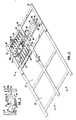
- Fig. 1 is an isometric view of a portion of a lead frame constructed in accordance with the principles of the present invention.
- Fig. 2 is a detail view illustrating a ground plane plate prior to folding while it is still connected to the lead frame.
- Fig. 3 is an isometric view illustrating the device paddle, ground plane plate, and signal leads of a lead frame after folding.
- Fig. 3A is an enlarged detail view showing a portion of Fig. 3.
- Fig. 4 is a sectional view taken along line 4-4 of Fig. 3, shown without the semiconductor device mounted on the device paddle.
- Fig. 5 is a sectional view similar to Fig. 4, shown with the semiconductor device mounted on the lead frame paddle, and the device encapsulated in plastic.
- Fig. 6 is a sectional view similar to Fig. 5, shown with the connecting tabs trimmed after folding.
- Referring to Figs. 1 and 2, a lead frame 10 constructed in accordance with the principles of the present invention includes a first
axial section 12 and a second axial section 14 defined by a centralaxial bar 16 and twoside bars axial section 12 includes a plurality ofindividual lead frames 22, there usually being from about 12 to 24individual frames 22 in a single lead frame strip 10. - The
individual lead frames 22 are generally conventional in construction and include adevice paddle 26, a pair of paddle supports 28a and 28b, and a plurality oflead fingers 30. Thepaddle 26 and paddle supports 28 are connected between the centralaxial bar 16 andside bar 18, while thelead fingers 30 are supported by atie bar 32 andtransverse frame bars 34. For reasons described more fully hereinbelow,paddle support 28b includes alock slot 36. - The second axial section 14 includes a plurality of
ground plane plates 40 suspended ontabs axial bar 16 andside bar 20.Tab 42b terminates in alock pin 43 which mates withlock slot 36 inpaddle support 28b, as will be described in more detail hereinafter. Theground plane plates 40 are aligned with theindividual lead frames 22 so that the connectingtab 42a of the plate is aligned with thepaddle support 28a of the frame.Notches 44 are formed in the centralaxial bar 16 adjacent the connection to connectingtab 42a, as best observed in Fig. 2. The notches facilitate severing thepaddle support 28a and connectingtab 42a from thebar 16 while leaving the tab and paddle support connected to each other. - The
ground plane plate 40 is generally rectangular having dimensions which exceed those of thepaddle 26 of thelead frame 22. Usually, the length and width of theground plane plate 40 will approximate the length and width of the final encapsulated package (as illustrated in Fig. 5). Theground plane plate 40 includesground connection tabs 46 located generally at each corner of its rectangular surface. Theconnection tabs 46 will extend outside of the final encapsulated package and will be used to connect the ground plane to ground on the mounting substrate, typically a printed circuit board. -
Ground plane plate 40 also includes a plurality ofbumps 50 formed in the surface. As illustrated in Figs. 1-2, thebumps 50 would extend downward away from the viewer so that, when theplate 40 is folded under thedevice paddle 26, thebumps 50 will project upward betweenadjacent lead fingers 30, as illustrated in Fig. 3. Conveniently, thebumps 50 will be formed by impressing theground plane 40, but may also be formed by an additive process.Plate 40 also includes a plurality ofholes 52 which allow the encapsulating material to penetrate the ground plane during transfer or injection molding. - The lead frame 10 will be formed from conventional materials, typically copper, a copper alloy, Kovar®, or Alloy 42, by conventional pressing and stamping techniques, or by etching. The dimensions of the frame, number of
lead fingers 30, and the like, are not critical. As illustrated, the lead frame is intended for a dual in-line package, but lead frames suitable for other packages, such as leaded quad packages, would also find use. - Referring now to Figs. 1-3, the plastic semiconductor package of the present invention is assembled by first folding the
ground plane plate 40 downward beneath thepaddle 26 of thelead frame 22. Usually, the paddle will be folded without severing the connection oftab 42a to centralaxial bar 16 so that the lead frame strip 10 remains essentially intact. To facilitate folding and accurately control the distance between thepaddle 26 andplate 40, thelock pin 43 of connectingtab 42b is folded upward and inserted intolock slot 36 onpaddle support 28b. Such folding results in the structure illustrated in Fig. 3, where theground plate 40 is attached to thelead frame 22 by the folded connectingtab 42a. - At the same time the
ground plane 40 is folded, theground connection tabs 46 may be folded in a stepped configuration, as illustrated in Fig. 3. Alternatively,ground connection tabs 46 may be folded after molding is completed in order to simplify the molding operation. Optionally, thepaddle support 26 may be depressed downward, as illustrated in Fig. 4. - After folding the
ground plane plate 40, asemiconductor die 60 is attached to thepaddle 26 by conventional techniques, such as using a glass frit, a thermally-conducting epoxy, or a gold-silicon eutectic alloy. After die attach, the bonding pads 62 on the die 60 are connected to thelead fingers 30 by conventional techniques, such as wire bonding or tape-automated bonding. See, Fig. 3A, whereexemplary wire bonds 63 are illustrated. Similarly, aground ring 64 on thedie 60 is connected to thebumps 50, either by wire bonding or tape-automated bonding (wire bonds 66 being illustrated). In the preferred arrangement illustrated, thebumps 50 lie between adjacentlead fingers 30 of thelead frame 22 so that the ground continuity continues between the lead fingers. By connecting thebumps 50 to theground ring 64, the ground is further continued between the adjacent signal bonding connections, e.g., the wire bonds or tape-automated bonds. In a further preferred embodiment, theground ring 64 includesspikes 65 which project inward between adjacent bonding pads 62. By connecting thebumps 50 directly to thesespikes 65, continuity of the ground is enhanced and inductive and capacitive coupling between signal leads is reduced. Such construction promises enhanced isolation of the entire length of the signal connections and reduced noise in the package. - After the bonding of the semiconductor die 60 to the
lead frame 22 andground plane 40 is complete, the package may be completed by encapsulation using a conventional solid matrix encapsulant 70 (Fig. 5). Conventional transfer or injection molding techniques are used to dispense the encapsulant around thelead frame 22 until thebonding wires connection tabs - Although the foregoing invention has been described in some detail by way of illustration and example for purposes of clarity of understanding, it will be obvious that certain changes and modifications may be practiced within the scope of the appended claims.
Claims (21)
a plurality of individual frames arranged in a row, each of said frames including a paddle, paddle supports, and a multiplicity of lead fingers circumscribing said paddle; and
a plurality of ground plane members, each ground plane member attached to an adjacent frame so that the frame may be folded to lie parallel to and spaced-apart from the paddle of each frame.
a first axial section including a plurality of individual frames, each frame including a paddle, a pair of paddle supports, and a multiplicity of lead fingers circumscribing the paddle; and
a second axial section including a plurality of ground planes arranged so that each ground plane lies adjacent an individual frame, whereby each ground plane may be folded to lie parallel to and spaced-apart from the paddle of each frame.
a paddle having two or more supports;
a semiconductor die mounted on the paddle;
a plurality of lead fingers circumscribing the paddle support;
a ground plane parallel to and spaced-apart from the paddle support, said ground plane having a plurality of bumps on its surface, wherein said bumps are arranged to project between adjacent leads; and
a solid matrix encapsulating the paddle support, semiconductor die, ground plane and a portion of each lead.
attaching a semiconductor die onto the paddle of a lead frame, said lead frame including a plurality of individual frames connected to ground plane members projecting laterally from the paddle supports;
folding the ground planes over to lie parallel to and spaced apart from the paddle support; and
encapsulating the die, lead frame, and paddle.
Applications Claiming Priority (2)
| Application Number | Priority Date | Filing Date | Title |
|---|---|---|---|
| US943339 | 1986-12-17 | ||
| US06/943,339 US4791473A (en) | 1986-12-17 | 1986-12-17 | Plastic package for high frequency semiconductor devices |
Publications (3)
| Publication Number | Publication Date |
|---|---|
| EP0272187A2 true EP0272187A2 (en) | 1988-06-22 |
| EP0272187A3 EP0272187A3 (en) | 1988-08-31 |
| EP0272187B1 EP0272187B1 (en) | 1992-10-28 |
Family
ID=25479483
Family Applications (1)
| Application Number | Title | Priority Date | Filing Date |
|---|---|---|---|
| EP87402883A Expired - Lifetime EP0272187B1 (en) | 1986-12-17 | 1987-12-17 | Plastic package for high frequency semiconductor devices |
Country Status (5)
| Country | Link |
|---|---|
| US (1) | US4791473A (en) |
| EP (1) | EP0272187B1 (en) |
| JP (1) | JPS63192260A (en) |
| KR (1) | KR960002497B1 (en) |
| DE (1) | DE3782406T2 (en) |
Cited By (3)
| Publication number | Priority date | Publication date | Assignee | Title |
|---|---|---|---|---|
| EP0560487A2 (en) * | 1992-02-07 | 1993-09-15 | Texas Instruments Incorporated | Semiconductor device having a lead frame |
| DE4318727A1 (en) * | 1992-06-05 | 1993-12-09 | Mitsubishi Electric Corp | Semiconductor device with lead-on-chip-structure - has brazing solder material with no moisture absorption, formed on surface of semiconductor component and fixed to support plate |
| EP0595600A1 (en) * | 1992-10-26 | 1994-05-04 | Texas Instruments Incorporated | Semiconductor device package |
Families Citing this family (52)
| Publication number | Priority date | Publication date | Assignee | Title |
|---|---|---|---|---|
| US5148243A (en) * | 1985-06-25 | 1992-09-15 | Hewlett-Packard Company | Optical isolator with encapsulation |
| US4863806A (en) * | 1985-06-25 | 1989-09-05 | Hewlett-Packard Company | Optical isolator |
| JP2522524B2 (en) * | 1988-08-06 | 1996-08-07 | 株式会社東芝 | Method for manufacturing semiconductor device |
| US5099306A (en) * | 1988-11-21 | 1992-03-24 | Honeywell Inc. | Stacked tab leadframe assembly |
| US5183711A (en) * | 1988-12-13 | 1993-02-02 | Shinko Electric Industries Co., Ltd. | Automatic bonding tape used in semiconductor device |
| US4965654A (en) * | 1989-10-30 | 1990-10-23 | International Business Machines Corporation | Semiconductor package with ground plane |
| US5008615A (en) * | 1989-11-03 | 1991-04-16 | Motorola, Inc. | Means and method for testing integrated circuits attached to a leadframe |
| US5386141A (en) * | 1992-03-31 | 1995-01-31 | Vlsi Technology, Inc. | Leadframe having one or more power/ground planes without vias |
| US5376909A (en) * | 1992-05-29 | 1994-12-27 | Texas Instruments Incorporated | Device packaging |
| DE4345301C2 (en) * | 1992-06-05 | 2003-11-20 | Mitsubishi Electric Corp | Lead wire frames for use in manufacturing a LOC structure semiconductor device and method of manufacturing a LOC structure semiconductor device |
| US5457340A (en) * | 1992-12-07 | 1995-10-10 | Integrated Device Technology, Inc. | Leadframe with power and ground planes |
| US5442225A (en) * | 1993-08-13 | 1995-08-15 | Lsi Logic Corporation | Integrated circuit having interconnects with ringing suppressing elements |
| EP0668615A1 (en) * | 1994-02-18 | 1995-08-23 | Siemens Aktiengesellschaft | Plastic SMD package for a semiconductor chip |
| US5485029A (en) * | 1994-06-30 | 1996-01-16 | International Business Machines Corporation | On-chip ground plane for semiconductor devices to reduce parasitic signal propagation |
| US5714792A (en) * | 1994-09-30 | 1998-02-03 | Motorola, Inc. | Semiconductor device having a reduced die support area and method for making the same |
| US5541565A (en) * | 1995-05-22 | 1996-07-30 | Trw Inc. | High frequency microelectronic circuit enclosure |
| US5969293A (en) * | 1997-07-18 | 1999-10-19 | National Semiconductor Corporation | Method and apparatus for doubling back single gauge lead frame |
| US6075283A (en) * | 1998-07-06 | 2000-06-13 | Micron Technology, Inc. | Downset lead frame for semiconductor packages |
| JP3444410B2 (en) * | 2000-03-23 | 2003-09-08 | 株式会社三井ハイテック | Lead frame and method of manufacturing semiconductor device |
| US6246312B1 (en) | 2000-07-20 | 2001-06-12 | Cts Corporation | Ball grid array resistor terminator network |
| SG112799A1 (en) | 2000-10-09 | 2005-07-28 | St Assembly Test Services Ltd | Leaded semiconductor packages and method of trimming and singulating such packages |
| US6686258B2 (en) | 2000-11-02 | 2004-02-03 | St Assembly Test Services Ltd. | Method of trimming and singulating leaded semiconductor packages |
| US6777786B2 (en) * | 2001-03-12 | 2004-08-17 | Fairchild Semiconductor Corporation | Semiconductor device including stacked dies mounted on a leadframe |
| US7038305B1 (en) | 2003-07-15 | 2006-05-02 | Altera Corp. | Package for integrated circuit die |
| US7180186B2 (en) * | 2003-07-31 | 2007-02-20 | Cts Corporation | Ball grid array package |
| US6946733B2 (en) * | 2003-08-13 | 2005-09-20 | Cts Corporation | Ball grid array package having testing capability after mounting |
| US7196313B2 (en) * | 2004-04-02 | 2007-03-27 | Fairchild Semiconductor Corporation | Surface mount multi-channel optocoupler |
| KR101297645B1 (en) | 2005-06-30 | 2013-08-20 | 페어차일드 세미컨덕터 코포레이션 | Semiconductor die package and method for making the same |
| US20090057852A1 (en) * | 2007-08-27 | 2009-03-05 | Madrid Ruben P | Thermally enhanced thin semiconductor package |
| US20070164428A1 (en) * | 2006-01-18 | 2007-07-19 | Alan Elbanhawy | High power module with open frame package |
| US7868432B2 (en) * | 2006-02-13 | 2011-01-11 | Fairchild Semiconductor Corporation | Multi-chip module for battery power control |
| US7768075B2 (en) | 2006-04-06 | 2010-08-03 | Fairchild Semiconductor Corporation | Semiconductor die packages using thin dies and metal substrates |
| US7656024B2 (en) | 2006-06-30 | 2010-02-02 | Fairchild Semiconductor Corporation | Chip module for complete power train |
| US7564124B2 (en) * | 2006-08-29 | 2009-07-21 | Fairchild Semiconductor Corporation | Semiconductor die package including stacked dice and heat sink structures |
| US7821116B2 (en) * | 2007-02-05 | 2010-10-26 | Fairchild Semiconductor Corporation | Semiconductor die package including leadframe with die attach pad with folded edge |
| US7659531B2 (en) * | 2007-04-13 | 2010-02-09 | Fairchild Semiconductor Corporation | Optical coupler package |
| US7902657B2 (en) * | 2007-08-28 | 2011-03-08 | Fairchild Semiconductor Corporation | Self locking and aligning clip structure for semiconductor die package |
| US20090057855A1 (en) * | 2007-08-30 | 2009-03-05 | Maria Clemens Quinones | Semiconductor die package including stand off structures |
| US20090140266A1 (en) * | 2007-11-30 | 2009-06-04 | Yong Liu | Package including oriented devices |
| US7589338B2 (en) * | 2007-11-30 | 2009-09-15 | Fairchild Semiconductor Corporation | Semiconductor die packages suitable for optoelectronic applications having clip attach structures for angled mounting of dice |
| KR20090062612A (en) * | 2007-12-13 | 2009-06-17 | 페어차일드코리아반도체 주식회사 | Multi chip package |
| US20090166826A1 (en) * | 2007-12-27 | 2009-07-02 | Janducayan Omar A | Lead frame die attach paddles with sloped walls and backside grooves suitable for leadless packages |
| US8106406B2 (en) | 2008-01-09 | 2012-01-31 | Fairchild Semiconductor Corporation | Die package including substrate with molded device |
| US20090194856A1 (en) * | 2008-02-06 | 2009-08-06 | Gomez Jocel P | Molded package assembly |
| KR101524545B1 (en) * | 2008-02-28 | 2015-06-01 | 페어차일드코리아반도체 주식회사 | Power device package and the method of fabricating the same |
| US7768108B2 (en) | 2008-03-12 | 2010-08-03 | Fairchild Semiconductor Corporation | Semiconductor die package including embedded flip chip |
| US8018054B2 (en) * | 2008-03-12 | 2011-09-13 | Fairchild Semiconductor Corporation | Semiconductor die package including multiple semiconductor dice |
| KR101519062B1 (en) * | 2008-03-31 | 2015-05-11 | 페어차일드코리아반도체 주식회사 | Semiconductor Device Package |
| US20090278241A1 (en) * | 2008-05-08 | 2009-11-12 | Yong Liu | Semiconductor die package including die stacked on premolded substrate including die |
| US8193618B2 (en) | 2008-12-12 | 2012-06-05 | Fairchild Semiconductor Corporation | Semiconductor die package with clip interconnection |
| US7973393B2 (en) | 2009-02-04 | 2011-07-05 | Fairchild Semiconductor Corporation | Stacked micro optocouplers and methods of making the same |
| US8421204B2 (en) | 2011-05-18 | 2013-04-16 | Fairchild Semiconductor Corporation | Embedded semiconductor power modules and packages |
Citations (4)
| Publication number | Priority date | Publication date | Assignee | Title |
|---|---|---|---|---|
| DE2818080A1 (en) * | 1977-04-26 | 1978-11-09 | Tokyo Shibaura Electric Co | ENCAPSULATED SEMICONDUCTOR DEVICE |
| EP0121268A1 (en) * | 1983-03-09 | 1984-10-10 | SGS MICROELETTRONICA S.p.A. | Flat-card-shaped semiconductor device with electric contacts on both faces and process for its manufacture |
| WO1984004648A1 (en) * | 1983-05-18 | 1984-11-22 | Mettler Rollin W Jun | Integrated circuit module and method of making same |
| EP0148083A2 (en) * | 1983-12-23 | 1985-07-10 | Fujitsu Limited | Ultra-high speed semiconductor integrated circuit device having a multi-layered wiring board |
Family Cites Families (6)
| Publication number | Priority date | Publication date | Assignee | Title |
|---|---|---|---|---|
| US4252864A (en) * | 1979-11-05 | 1981-02-24 | Amp Incorporated | Lead frame having integral terminal tabs |
| US4477827A (en) * | 1981-02-02 | 1984-10-16 | Northern Telecom Limited | Lead frame for leaded semiconductor chip carriers |
| US4551746A (en) * | 1982-10-05 | 1985-11-05 | Mayo Foundation | Leadless chip carrier apparatus providing an improved transmission line environment and improved heat dissipation |
| JPS5989438A (en) * | 1982-11-15 | 1984-05-23 | Nippon Denso Co Ltd | Semiconductor device |
| US4680613A (en) * | 1983-12-01 | 1987-07-14 | Fairchild Semiconductor Corporation | Low impedance package for integrated circuit die |
| US4651415A (en) * | 1985-03-22 | 1987-03-24 | Diacon, Inc. | Leaded chip carrier |
-
1986
- 1986-12-17 US US06/943,339 patent/US4791473A/en not_active Expired - Lifetime
-
1987
- 1987-12-11 KR KR1019870014138A patent/KR960002497B1/en not_active IP Right Cessation
- 1987-12-17 JP JP62317608A patent/JPS63192260A/en active Pending
- 1987-12-17 EP EP87402883A patent/EP0272187B1/en not_active Expired - Lifetime
- 1987-12-17 DE DE8787402883T patent/DE3782406T2/en not_active Expired - Fee Related
Patent Citations (4)
| Publication number | Priority date | Publication date | Assignee | Title |
|---|---|---|---|---|
| DE2818080A1 (en) * | 1977-04-26 | 1978-11-09 | Tokyo Shibaura Electric Co | ENCAPSULATED SEMICONDUCTOR DEVICE |
| EP0121268A1 (en) * | 1983-03-09 | 1984-10-10 | SGS MICROELETTRONICA S.p.A. | Flat-card-shaped semiconductor device with electric contacts on both faces and process for its manufacture |
| WO1984004648A1 (en) * | 1983-05-18 | 1984-11-22 | Mettler Rollin W Jun | Integrated circuit module and method of making same |
| EP0148083A2 (en) * | 1983-12-23 | 1985-07-10 | Fujitsu Limited | Ultra-high speed semiconductor integrated circuit device having a multi-layered wiring board |
Non-Patent Citations (3)
| Title |
|---|
| PATENT ABSTRACTS OF JAPAN, vol. 10, no. 289 (E-442)[2345], 2nd October 1986; & JP-A-61 108 157 (MATSUSHITA ELECTRIC IND. CO., LTD.) 26-05-1986 * |
| PATENT ABSTRACTS OF JAPAN, vol. 6, no. 132 (E-119)[1010], 17th July 1982; & JP-A-57 056 953 (NIPPON DENKI K.K.) 05-04-1982 * |
| PATENT ABSTRACTS OF JAPAN, vol. 9, no. 169 (E-328)[1892], 13th July 1985; & JP-A-60 043 849 (FUJI DENKI SEIZO K.K.) 08-03-1985 * |
Cited By (11)
| Publication number | Priority date | Publication date | Assignee | Title |
|---|---|---|---|---|
| EP0560487A2 (en) * | 1992-02-07 | 1993-09-15 | Texas Instruments Incorporated | Semiconductor device having a lead frame |
| EP0560487A3 (en) * | 1992-02-07 | 1993-12-08 | Texas Instruments Inc | Semiconductor device having a lead frame |
| US5804871A (en) * | 1992-02-07 | 1998-09-08 | Texas Instruments Incorporated | Lead on chip semiconductor device having bus bars and crossing leads |
| DE4318727A1 (en) * | 1992-06-05 | 1993-12-09 | Mitsubishi Electric Corp | Semiconductor device with lead-on-chip-structure - has brazing solder material with no moisture absorption, formed on surface of semiconductor component and fixed to support plate |
| US5535509A (en) * | 1992-06-05 | 1996-07-16 | Mitsubishi Denki Kabushiki Kaisha | Method of making a lead on chip (LOC) semiconductor device |
| US5724726A (en) * | 1992-06-05 | 1998-03-10 | Mitsubishi Denki Kabushiki Kaisha | Method of making leadframe for lead-on-chip (LOC) semiconductor device |
| DE4318727C2 (en) * | 1992-06-05 | 1998-03-12 | Mitsubishi Electric Corp | Process for the production of a semiconductor device with LOC structure and associated leadframe |
| US5763829A (en) * | 1992-06-05 | 1998-06-09 | Mitsubishi Denki Kabushiki Kaisha | Leadframe including frame-cutting slit for lead-on-chip (LOC) semiconductor device and semiconductor device incorporating the leadframe |
| US5900582A (en) * | 1992-06-05 | 1999-05-04 | Mitsubishi Denki Kabushiki Kaisha | Lead frame including frame-cutting slit for lead-on-chip (LOC) semiconductor device and semiconductor device incorporating the lead frame |
| EP0595600A1 (en) * | 1992-10-26 | 1994-05-04 | Texas Instruments Incorporated | Semiconductor device package |
| US5663597A (en) * | 1992-10-26 | 1997-09-02 | Texas Instruments Incorporated | RF device package for high frequency applications |
Also Published As
| Publication number | Publication date |
|---|---|
| US4791473A (en) | 1988-12-13 |
| EP0272187A3 (en) | 1988-08-31 |
| KR880008440A (en) | 1988-08-31 |
| DE3782406T2 (en) | 1993-05-06 |
| JPS63192260A (en) | 1988-08-09 |
| KR960002497B1 (en) | 1996-02-17 |
| DE3782406D1 (en) | 1992-12-03 |
| EP0272187B1 (en) | 1992-10-28 |
Similar Documents
| Publication | Publication Date | Title |
|---|---|---|
| US4791473A (en) | Plastic package for high frequency semiconductor devices | |
| US6175149B1 (en) | Mounting multiple semiconductor dies in a package | |
| EP0228869B1 (en) | Method of manufacturing an electronic component package | |
| US5332864A (en) | Integrated circuit package having an interposer | |
| US6297547B1 (en) | Mounting multiple semiconductor dies in a package | |
| US9159588B2 (en) | Packaged leadless semiconductor device | |
| KR900002908B1 (en) | Resin-sealed simiconductor device | |
| US7102209B1 (en) | Substrate for use in semiconductor manufacturing and method of making same | |
| US5444301A (en) | Semiconductor package and method for manufacturing the same | |
| US4974057A (en) | Semiconductor device package with circuit board and resin | |
| US5639694A (en) | Method for making single layer leadframe having groundplane capability | |
| US4891687A (en) | Multi-layer molded plastic IC package | |
| EP0774162B1 (en) | Manufacturing dual sided wire bonded integrated circuit chip packages using offset wire bonds and support block cavities | |
| EP0554893B1 (en) | Partially-molded, PCB chip carrier package and method of forming same | |
| KR100328143B1 (en) | Lead frame with layered conductive plane | |
| US7489021B2 (en) | Lead frame with included passive devices | |
| KR19990029974A (en) | Single leadframe package having a combined induction coil and an integrated circuit semiconductor chip, and a method of manufacturing the same | |
| JPH06224246A (en) | High multiterminal package for semiconductor element | |
| US20070099344A1 (en) | Ultrathin leadframe BGA circuit package | |
| US6677665B2 (en) | Dual-die integrated circuit package | |
| US6791166B1 (en) | Stackable lead frame package using exposed internal lead traces | |
| US6331452B1 (en) | Method of fabricating integrated circuit package with opening allowing access to die | |
| GB2199988A (en) | Multi-layer molded plastic ic package | |
| EP0698922B1 (en) | Leadframe for supporting integrated semiconductor devices | |
| JP3495566B2 (en) | Semiconductor device |
Legal Events
| Date | Code | Title | Description |
|---|---|---|---|
| PUAI | Public reference made under article 153(3) epc to a published international application that has entered the european phase |
Free format text: ORIGINAL CODE: 0009012 |
|
| AK | Designated contracting states |
Kind code of ref document: A2 Designated state(s): DE FR GB IT NL |
|
| PUAL | Search report despatched |
Free format text: ORIGINAL CODE: 0009013 |
|
| AK | Designated contracting states |
Kind code of ref document: A3 Designated state(s): DE FR GB IT NL |
|
| 17P | Request for examination filed |
Effective date: 19890222 |
|
| 17Q | First examination report despatched |
Effective date: 19910318 |
|
| GRAA | (expected) grant |
Free format text: ORIGINAL CODE: 0009210 |
|
| AK | Designated contracting states |
Kind code of ref document: B1 Designated state(s): DE FR GB IT NL |
|
| ITF | It: translation for a ep patent filed |
Owner name: STUDIO TORTA SOCIETA' SEMPLICE |
|
| REF | Corresponds to: |
Ref document number: 3782406 Country of ref document: DE Date of ref document: 19921203 |
|
| ET | Fr: translation filed | ||
| PLBE | No opposition filed within time limit |
Free format text: ORIGINAL CODE: 0009261 |
|
| STAA | Information on the status of an ep patent application or granted ep patent |
Free format text: STATUS: NO OPPOSITION FILED WITHIN TIME LIMIT |
|
| 26N | No opposition filed | ||
| PGFP | Annual fee paid to national office [announced via postgrant information from national office to epo] |
Ref country code: GB Payment date: 19941111 Year of fee payment: 8 |
|
| PGFP | Annual fee paid to national office [announced via postgrant information from national office to epo] |
Ref country code: FR Payment date: 19941209 Year of fee payment: 8 |
|
| PGFP | Annual fee paid to national office [announced via postgrant information from national office to epo] |
Ref country code: NL Payment date: 19941231 Year of fee payment: 8 |
|
| PG25 | Lapsed in a contracting state [announced via postgrant information from national office to epo] |
Ref country code: GB Effective date: 19951217 |
|
| PG25 | Lapsed in a contracting state [announced via postgrant information from national office to epo] |
Ref country code: NL Effective date: 19960701 |
|
| GBPC | Gb: european patent ceased through non-payment of renewal fee |
Effective date: 19951217 |
|
| PG25 | Lapsed in a contracting state [announced via postgrant information from national office to epo] |
Ref country code: FR Effective date: 19960830 |
|
| NLV4 | Nl: lapsed or anulled due to non-payment of the annual fee |
Effective date: 19960701 |
|
| REG | Reference to a national code |
Ref country code: FR Ref legal event code: ST |
|
| PG25 | Lapsed in a contracting state [announced via postgrant information from national office to epo] |
Ref country code: IT Free format text: LAPSE BECAUSE OF NON-PAYMENT OF DUE FEES;WARNING: LAPSES OF ITALIAN PATENTS WITH EFFECTIVE DATE BEFORE 2007 MAY HAVE OCCURRED AT ANY TIME BEFORE 2007. THE CORRECT EFFECTIVE DATE MAY BE DIFFERENT FROM THE ONE RECORDED. Effective date: 20051217 |
|
| PGFP | Annual fee paid to national office [announced via postgrant information from national office to epo] |
Ref country code: DE Payment date: 20060131 Year of fee payment: 19 |
|
| PG25 | Lapsed in a contracting state [announced via postgrant information from national office to epo] |
Ref country code: DE Free format text: LAPSE BECAUSE OF NON-PAYMENT OF DUE FEES Effective date: 20070703 |