EP0147587A2 - Sichtbarmachen von Defekten in einem Halbleiterkörper - Google Patents
Sichtbarmachen von Defekten in einem Halbleiterkörper Download PDFInfo
- Publication number
- EP0147587A2 EP0147587A2 EP84113502A EP84113502A EP0147587A2 EP 0147587 A2 EP0147587 A2 EP 0147587A2 EP 84113502 A EP84113502 A EP 84113502A EP 84113502 A EP84113502 A EP 84113502A EP 0147587 A2 EP0147587 A2 EP 0147587A2
- Authority
- EP
- European Patent Office
- Prior art keywords
- electrode
- imaging
- wafer
- linear electrode
- recited
- Prior art date
- Legal status (The legal status is an assumption and is not a legal conclusion. Google has not performed a legal analysis and makes no representation as to the accuracy of the status listed.)
- Granted
Links
Images
Classifications
-
- G—PHYSICS
- G01—MEASURING; TESTING
- G01R—MEASURING ELECTRIC VARIABLES; MEASURING MAGNETIC VARIABLES
- G01R31/00—Arrangements for testing electric properties; Arrangements for locating electric faults; Arrangements for electrical testing characterised by what is being tested not provided for elsewhere
- G01R31/28—Testing of electronic circuits, e.g. by signal tracer
- G01R31/302—Contactless testing
- G01R31/308—Contactless testing using non-ionising electromagnetic radiation, e.g. optical radiation
-
- G—PHYSICS
- G01—MEASURING; TESTING
- G01R—MEASURING ELECTRIC VARIABLES; MEASURING MAGNETIC VARIABLES
- G01R31/00—Arrangements for testing electric properties; Arrangements for locating electric faults; Arrangements for electrical testing characterised by what is being tested not provided for elsewhere
- G01R31/26—Testing of individual semiconductor devices
- G01R31/265—Contactless testing
- G01R31/2656—Contactless testing using non-ionising electromagnetic radiation, e.g. optical radiation
Definitions
- the invention relates generally to imaging defects in a semiconductor body, and is concerned, in particular, with a method-and apparatus for inspecting for crystallographic defects in the region near the surface.
- the location of the fault or defect can be localized within a complex integrated circuit by scanning a completed circuit with a small beam of radiation.
- Lockhart et al. in US Patent No. 4,309,657 raster scan an electron beam over the integrated circuit.
- Ager et al. in UK Patent Application No. 2,069,152 perform a similar scan with a lasar beam over an integrated circuit for which the supply voltage is reduced to a minimum level. While both of these methods are useful for pinpointing the location of a defect, they still require complicated electronic testing equipment and further require that the integrated circuit be completely fabricated. Furthermore, their methods, being electrical tests, do not provide information as to the type of defect causing the problem.
- Zerbst type measurements yield little or no information about the density or distribution of the defects on the surface. Finally, electrical probing is tedious and expensive. The wafer must be oxidized and then metallized with the aluminum dots. The individual dots must then be separately probed and analysed.
- Yet a further object of this invention is to provide rapid defect imaging with high resolution over a large surface area of semiconductor material.
- the invention can be summarized as a method and apparatus for imaging large area semiconductors by oxidizing at least one side of a semiconductor wafer, pre-treating both surfaces in a corona discharge and then passing the wafer beneath a linear electrode extending across the wafer and scanning a laser beam through an aperture and along the length of the linear electrode.
- Signals picked up by the linear electrode are proportional to the local minority carrier lifetime and can be imaged in synchronism with the laser scan and the wafer translation to provide an image of the surface recombination center defects in the wafer.
- the linear electrode may be bifurcated, with the scan aperture running between the two linear arms of the electrode. This configuration increases the coupling of the photo-voltage signal to the detector electronics.
- a semiconductor material 10 has a conduction band 12 and a valence band 14 separated by the semicondcutor band-gap. If the semiconductor is p-type as illustrated, a Fermi level 16 lies relatively close to the valence band 14.
- the semiconductor 10 is overlaid with an oxide layer 18. Two types of positive charges are introduced into the oxide layer 18, charged surface states 20 and surface charge 22. The net effect of the charge is to bend the bands 12 and 14 relative to the Fermi level 16. Light penetrated into the semiconductor 10 through the oxide 18 creates electron-hole pairs.
- the negatively charged electrons are attracted to the surface of the semiconductor by the positive charge 20 and 22 in the oxide 18, while the positively charged holes are repelled into the bulk of the semiconductor.
- the electrons are minority carriers in p-type semiconductors. When they reach the interface between the semiconductor 10 and the oxide 18, they are measured by an apparatus to be described later. However, the number of electrons reaching the interface is determined by the minority lifetime or, alternatively, the recombination rate. Therefore in an area of the semiconductor 10, where a defect causes increased recombination or decreased minority lifetime, the number of electrons reaching the interface is reduced with a corresponding reduction in the signal. Thus a map of the detected signal of electrons at the surface will be an inverse map of the defect distribution affecting the minority lifetime in the semiconductor.
- the wafer is first oxidized, both front and back although it has been found that oxidizing only the imaged surface still produces satisfactory results.
- the naturally occurring native oxide of silicon provides a satisfactory oxide so that a separate oxidizing step is not required as long as the silicon has been exposed to oxygen.
- a wet or dry oxidizing step may be used. It has been found that if the silicon wafer already has had a metallization layer applied, the metallization does not interfere with the imaging of the neighbouring oxidized silicon. In typical integrated circuit processing, even the metallization is covered with an oxide layer.
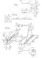
- the silicon wafer is pretreated by being passed through a corona discharge station schematically illustrated in Fig 2.
- the corona discharge station is composed of an upper corona discharge device 30 and a lower corona discharge device 32.
- Each of these corona discharge devices comprises a discharge rod 34 or 35 electrically connected to a DC high voltage power source 36 or 37 of appropriate polarity.
- Surrounding the discharge rod 34 or 35 is a cylindrically shaped, conductive housing 38 or 40.
- the lower section of the housing 38 of the upper corona discharge device 30 is replaced with a conductive mesh 42 that is also electrically connected-to the cylindrical housing 38.
- the electrical potential of the cylindrical housing 38 and its associated mesh 42 is determined by a variable DC power source 44.
- the cylindrical housing 40 of the lower discharge device 32 has an upward facing conductive mesh 46 and a DC power supply 44 of the upper device 30.
- the axial extent of the two cylindrical housings 38 and 40 is sufficient to allow an entire semiconductor wafer to pass between the meshes 42 and 46.
- the opposing ends of each housing '38 or 40 are covered by caps (not shown).
- the upper and lower devices 3& and 32 are separated so that there is a distance of approximately 1 cm between the meshes 42 and 46.
- Nitrogen gas is introduced through tubes 50 and 52 so that it penetrates the housings 38 and 40 and flows over the discharge rods 34 and 35.
- An inert gas such as argon, neon, krypton or other non-reacting gases may alternatively be used for carrying the discharge.
- the discharge rods 34 and 35 ionize the gas as it moves toward and through the respective meshes 42 and 46.
- the surface of the semiconductor material is influenced by either charged surface states or surface charge in the oxide of the respective side of the wafer. It is not known what the distribution of charge is between the surface states and the surface charges but it is believed that both occur.
- the characteristics of the oxide are determined by the voltages applied by the DC power supplies 44 and 48 and these values can be varied to optimize the contrast in the obtained image.
- a somewhat different device for corona charging of semiconductor devices is provided by Szeden in US Patent No. 4,326,165.
- the oxidized silicon wafer After the oxidized silicon wafer has been pretreated in the corona discharge station, it is taken to the scanning station illustrated schematically in Figs 2(a) and 2(b). In practice, the wafer moves along a track at constant speed through the corona discharge station and from there to the scanning station, all at a constant speed of about 1 cm/sec. Many of the details of the scanning station are disclosed in the aforementioned article by Philbrick et al.
- a laser 60 produces a narrow beam cf light at a wavelength of 632.8 nm. At this wavelength, light penetrates into silicon a distance of 1.9 ⁇ m.
- the laser intensity is in the range of 1-10 mW.
- the laser beam is reflected from a mirror 62 which can be rotated about an axis 64 to produce a linear scan.
- a lens 66 focuses the laser beam to about 25 ⁇ m at the surface of a wafer 68.
- the focused laser beam is scanned between and along the length of the arms of a bifurcated electrode 70 extending across the wafer 68 transverse to the mechanical movement or slow scan of the wafer.
- the bifurcated electrode 70 is spaced above the wafer 68 by a distance of between 100 and 500 um.
- the bifurcated electrode 70 is electrically connected to a preamplifier 72 which controls the display on a display system 74.
- the detection in the preamplifier 72 may be either voltage mode or current mode.
- the display system 74 which can use the techniques disclosed by Philbrick et al., has one axis of its display synchronizd with the scanning of the laser beam and other axis synchronized with the mechanical movement of the wafer 68.
- a ground electrode 76 is in the same plane as the bifurcated electrode 70 and surrounds it.
- the ground electrode 76 establishes a ground plane for the detected area of the wafer. It may extend much further away from the bifurcated electrode 70.
- the ground electrode may be connected to another grounding plate located between the bifucated electrode and the lens 66 through an aperture of which the laser beam can shine.
- the ground of the ground electrode 76 is used by the preamplifier 72 as a reference for the detected signal.
- the princip ⁇ ê of operation for the imaging of defects is illustrated in the cross-sectional view of Fig 3 in which the wafer 68 is composed of the semiconductor 10 and the overlying oxide layer 12.
- the lower oxide layer at the bottom of the semiconductor 10 is not illustrated in this figure.
- the charged surface states 20 and the surface charge 22 were established in the oxide at the corona discharge station. This charge 20 and 22 establishes the surface conditions on the wafer 68.
- the laser beam directed onto the surface of the wafer 68 through the aperture of the bifurcated electrode 70 produces charge 80, in this case minority carriers, at the interface between the semiconductor 10 and the oxide 12 in the vicinity of the electrode aperture.
- the amount of the charge 80 at the interface is directly related to the minority carrier lifetime and is thus reduced when there are recombination defects in the vicinity of the laser beam.
- the charge at the interface 80 produces an image charge 82 in the bifurcated electrode 70. It is believed that the charge 80 at the interface is only partially imaged by the electrode charge 82 but it is not known what fraction is imaged. However, the presence of a defect will reduce the interface charge 80 with a corresponding decrease in the electrode charge 82.
- the electrode charge 82 is detected by the preamplifier 72-and displayed in the display system 74.
- the bandwidth of the detector system extends from 1 kHz to 10 MHz.
- the laser beam is scanned along the length of the bifurcated electrode at about two hundred scans per second.
- the wafer 68 is moving at a speed of apprcximately 1 cm/sec transversely to the scan of the laser beam. It has been found that with the laser beam focused to about 25 ⁇ m the image of defects on the wafer is resolved to between 50 and 250 um.
- a resin-filled board'90 serves as a support for the bifurcated electrode 70 and the ground electrode 76.
- the resin-filled board is insulating and is as thin as possible, consistent with the requirement of mechanical stability.
- a slit 92 of about 250 ⁇ m in width is cut along a portion of the resin-filled board 90. The slit 92 does not extend to the ends of the board 90 in order to provide mechanical integrity.
- the electrodes 70 and 76 of a conductive material like aluminum, are deposited onto the board 90 in the pattern illustrated in Fig 2.
- the width of each arm of the bifurcated electrode 70 is about 1,000 ⁇ m, although this dimension can be varied between 250 and 2,500 ⁇ m.
- the width of the arms of the ground electrode 76 are made the same as that of the arms of the bifurcated electrode 70 but, if desired, can be made much wider.
- both ends of the board 90 are mechanically fixed and the wafer 68 slowly passes beneath the electrode assembly. It has been found that a separation of 50 to 500 um between the electrodes 70 and 76 and the upper surface of the wafer 68 produces good resolution of defects in the photo-voltage image.
- the contrast of the image can be optimized by varying the surface potential induced by the corona discharge station.
- the corona current can be varied to yield differing amounts of ultraviolet radiation and ionized gas current and the voltage on the meshes 42 and 46 can be varied. It has been found that operating the meshes at ⁇ 20 V produces high contrast images but voltages between 5 and 100 V may be employed depending upon the sample.
- Signal optimization is believed to be based upon depleting the surface of the semiconductor 10 of majority carriers but not so much as to heavily accumulate a minority charge. That is, to produce an optimum image, the valence and conduction bands 12 and 14 should be bent sufficiently by the corona induced charge 20 and 22 so that the Fermi level 16 lies approximately at mid-gap at the interface.
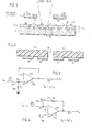
- Figs 5 and 6 Two preamplifier options are illustrated in Figs 5 and 6. Both the voltage mode illustrated in Fig 5 and the current mode illustrated in Fig 6 use an operational amplifier integrated circuit and operate in accordance with basic operational amplifier theory. (Reference "Operational Amplifiers - Theory and Practice" by Roberge and published by Wiley).
- the electrode charge 82 causes a current 102 to flow through a resistor 104, connected between the noninverting input of an operational amplifier 106 and ground, producing a voltage drop E in 108.
- the output of the amplifier 106 is directly connected to its inverting input.
- a preamplifier 72a thus has a voltage gain of one and, therefore, the output voltage E o 110 will equal the voltage drop E. in 108.
- a current mode preamplifier 72b shown in Fig 6 has its inverting input 112 of an operational amplifier 114 at virtually the same potential as its non-inverting input 116 which is common ground.
- the electrode charge 82 causes a current I in 118 to flow into a node 120 connected to the inverting input 112 and separated from the output of the amplifier 114 by a resistor 122. Since the input impedance of the inverting input 112 is very high compared to common ground, an equal current I 124 leaves the node 120 and flows through the resistor 122 producing an output voltage E 126.
- the current mode preamplifier 72b of Fig 6 is the preferred configuration since it is a low impedance circuit and hence exhibits higher signal to noise ratio, higher gain-bandwidth, and lower susceptibility to externally generated noise.
- the ground electrode 76 surrounding the bifurcated electrode is a ground plane which is spaced 100-1000 ⁇ m above the wafer 68. This ground electrode 76 is connected to the ground return on the preamplifier 72.
- the wafer 68 is insulated from ground so that the ground plane electrode 76 determines the potential on the wafer 68. An additional ground plane above the bifurcated electrode 7C will reduce noise in the signal.
- the method can be extended to n-type silicon and even to other types of semiconductor material by appropriate changes in the corona discharge conditions.
- the upper discharge rod 34 is connected to a positive high voltage source 36 and the lower discharge rod 35 is connected to a negative high voltage source 37.
- the upper and lower discharge rods 34 and 35 are connected to negative and positive high voltage supplies, respectively.
- both sides of the wafer 68 be subjected to corona charging or pretreatment, it is nontheless possible to obtain satisfactory imaging by charging only one side of the wafer. In that case, however, a ground plane needs to be established on the uncharged side of the wafer.
- the surface conductivity of the wafer can be increased and an improved resolution obtained if an auxiliary DC light source floods the area of the wafer being scanned by the laser beam.
- the DC power supply to the DC light source should be regulated. It is believed that the increased surface conductivity produces an increased coupling of the surface photo-voltage to the bifurcated electrode. This method improves resolution at the expense of reduced contrast.
- the detection technique described for the preferred embodiment is a DC illumination technique in which the charge on the bifurcated electrode 70 is measured and variations in that signal are imaged in the display system.
- the sensitivity of detection can be increased by instead using an AC illumination technique in which the laser beam is chopped at a given frequency and then the detection system detects signals only at that frequency.
- the chopping can be performed in the range of 10 to 50 MHz.
- the photovoltaic imaging is far superior to the electrical tests in characterizing recombination center defects in silicon wafers.
- the test is both fast and non-destructive and allows the characterization of every wafer put through the fabrication line.
- the photo-voltaic test is able to probe the entire wafer surface and to image the defects in order that they may be characterized and identified. Tests can be made on wafers at the incoming inspection and also after the first several high temperature processing steps.
- test can be used with partially fabricated wafers and even with wafers whose fabrication has been completed, including metallization.
- the patterns of the fabrication show in the imaging but the underlying show through as well. It is also possible to image the unfabricated side of a wafer. This technique would detect slip-lines extending through the wafer from the fabricated side.
- the backside inspection has the advantage of suppressing the fabricated circuit patterns.
Landscapes
- Physics & Mathematics (AREA)
- Health & Medical Sciences (AREA)
- Engineering & Computer Science (AREA)
- Electromagnetism (AREA)
- Toxicology (AREA)
- General Physics & Mathematics (AREA)
- Computer Vision & Pattern Recognition (AREA)
- General Engineering & Computer Science (AREA)
- Investigating Or Analyzing Materials By The Use Of Electric Means (AREA)
- Testing Or Measuring Of Semiconductors Or The Like (AREA)
- Investigating Materials By The Use Of Optical Means Adapted For Particular Applications (AREA)
Applications Claiming Priority (2)
| Application Number | Priority Date | Filing Date | Title |
|---|---|---|---|
| US06/561,364 US4599558A (en) | 1983-12-14 | 1983-12-14 | Photovoltaic imaging for large area semiconductors |
| US561364 | 2000-04-28 |
Publications (3)
| Publication Number | Publication Date |
|---|---|
| EP0147587A2 true EP0147587A2 (de) | 1985-07-10 |
| EP0147587A3 EP0147587A3 (en) | 1986-12-30 |
| EP0147587B1 EP0147587B1 (de) | 1990-01-17 |
Family
ID=24241638
Family Applications (1)
| Application Number | Title | Priority Date | Filing Date |
|---|---|---|---|
| EP84113502A Expired EP0147587B1 (de) | 1983-12-14 | 1984-11-09 | Sichtbarmachen von Defekten in einem Halbleiterkörper |
Country Status (4)
| Country | Link |
|---|---|
| US (1) | US4599558A (de) |
| EP (1) | EP0147587B1 (de) |
| JP (1) | JPS60128630A (de) |
| DE (1) | DE3481086D1 (de) |
Families Citing this family (71)
| Publication number | Priority date | Publication date | Assignee | Title |
|---|---|---|---|---|
| US4698587A (en) * | 1985-03-28 | 1987-10-06 | The United States Of America As Represented By The Secretary Of The Air Force | Method of characterizing critical timing paths and analyzing timing related failure modes in very large scale integrated circuits |
| JPH01245527A (ja) * | 1988-03-26 | 1989-09-29 | Shin Etsu Handotai Co Ltd | シリコン酸化膜界面の特性均一化方法 |
| US5306345A (en) * | 1992-08-25 | 1994-04-26 | Particle Solutions | Deposition chamber for deposition of particles on semiconductor wafers |
| US5427644A (en) * | 1993-01-11 | 1995-06-27 | Tokyo Seimitsu Co., Ltd. | Method of manufacturing semiconductor wafer and system therefor |
| US5498974A (en) * | 1994-12-30 | 1996-03-12 | International Business Machines Corporation | Contactless corona-oxide-semiconductor Q-V mobile charge measurement method and apparatus |
| US5661408A (en) * | 1995-03-01 | 1997-08-26 | Qc Solutions, Inc. | Real-time in-line testing of semiconductor wafers |
| US5594247A (en) * | 1995-07-07 | 1997-01-14 | Keithley Instruments, Inc. | Apparatus and method for depositing charge on a semiconductor wafer |
| US5773989A (en) * | 1995-07-14 | 1998-06-30 | University Of South Florida | Measurement of the mobile ion concentration in the oxide layer of a semiconductor wafer |
| US5907764A (en) * | 1995-11-13 | 1999-05-25 | Advanced Micro Devices, Inc. | In-line detection and assessment of net charge in PECVD silicon dioxide (oxide) layers |
| US5767693A (en) * | 1996-09-04 | 1998-06-16 | Smithley Instruments, Inc. | Method and apparatus for measurement of mobile charges with a corona screen gun |
| US6037797A (en) * | 1997-07-11 | 2000-03-14 | Semiconductor Diagnostics, Inc. | Measurement of the interface trap charge in an oxide semiconductor layer interface |
| US5977788A (en) * | 1997-07-11 | 1999-11-02 | Lagowski; Jacek | Elevated temperature measurement of the minority carrier lifetime in the depletion layer of a semiconductor wafer |
| US6060709A (en) * | 1997-12-31 | 2000-05-09 | Verkuil; Roger L. | Apparatus and method for depositing uniform charge on a thin oxide semiconductor wafer |
| US6325078B2 (en) | 1998-01-07 | 2001-12-04 | Qc Solutions, Inc., | Apparatus and method for rapid photo-thermal surface treatment |
| NL1013204C2 (nl) * | 1999-10-04 | 2001-04-05 | Stichting Energie | Inrichting voor het lokaliseren van productiefouten in een fotovolta´sch element. |
| WO2001086698A2 (en) | 2000-05-10 | 2001-11-15 | Kla-Tencor, Inc. | Method and system for detecting metal contamination on a semiconductor wafer |
| US6891627B1 (en) | 2000-09-20 | 2005-05-10 | Kla-Tencor Technologies Corp. | Methods and systems for determining a critical dimension and overlay of a specimen |
| US7130029B2 (en) | 2000-09-20 | 2006-10-31 | Kla-Tencor Technologies Corp. | Methods and systems for determining an adhesion characteristic and a thickness of a specimen |
| US6812045B1 (en) | 2000-09-20 | 2004-11-02 | Kla-Tencor, Inc. | Methods and systems for determining a characteristic of a specimen prior to, during, or subsequent to ion implantation |
| US6919957B2 (en) | 2000-09-20 | 2005-07-19 | Kla-Tencor Technologies Corp. | Methods and systems for determining a critical dimension, a presence of defects, and a thin film characteristic of a specimen |
| US6782337B2 (en) | 2000-09-20 | 2004-08-24 | Kla-Tencor Technologies Corp. | Methods and systems for determining a critical dimension an a presence of defects on a specimen |
| US6673637B2 (en) | 2000-09-20 | 2004-01-06 | Kla-Tencor Technologies | Methods and systems for determining a presence of macro defects and overlay of a specimen |
| AU2001295060A1 (en) | 2000-09-20 | 2002-04-02 | Kla-Tencor-Inc. | Methods and systems for semiconductor fabrication processes |
| US7349090B2 (en) | 2000-09-20 | 2008-03-25 | Kla-Tencor Technologies Corp. | Methods and systems for determining a property of a specimen prior to, during, or subsequent to lithography |
| US6694284B1 (en) | 2000-09-20 | 2004-02-17 | Kla-Tencor Technologies Corp. | Methods and systems for determining at least four properties of a specimen |
| US7106425B1 (en) | 2000-09-20 | 2006-09-12 | Kla-Tencor Technologies Corp. | Methods and systems for determining a presence of defects and a thin film characteristic of a specimen |
| US6734696B2 (en) * | 2001-11-01 | 2004-05-11 | Kla-Tencor Technologies Corp. | Non-contact hysteresis measurements of insulating films |
| JP3853708B2 (ja) * | 2002-07-10 | 2006-12-06 | Necアクセステクニカ株式会社 | デジタル画像符号化装置および符号化方法ならびにプログラム |
| US7012438B1 (en) | 2002-07-10 | 2006-03-14 | Kla-Tencor Technologies Corp. | Methods and systems for determining a property of an insulating film |
| US7968354B1 (en) | 2002-10-04 | 2011-06-28 | Kla-Tencor Technologies Corp. | Methods for correlating backside and frontside defects detected on a specimen and classification of backside defects |
| US7064565B1 (en) | 2002-10-31 | 2006-06-20 | Kla-Tencor Technologies Corp. | Methods and systems for determining an electrical property of an insulating film |
| US7248062B1 (en) | 2002-11-04 | 2007-07-24 | Kla-Tencor Technologies Corp. | Contactless charge measurement of product wafers and control of corona generation and deposition |
| US7075318B1 (en) | 2003-01-16 | 2006-07-11 | Kla-Tencor Technologies Corp. | Methods for imperfect insulating film electrical thickness/capacitance measurement |
| US6911350B2 (en) * | 2003-03-28 | 2005-06-28 | Qc Solutions, Inc. | Real-time in-line testing of semiconductor wafers |
| US6909291B1 (en) | 2003-06-24 | 2005-06-21 | Kla-Tencor Technologies Corp. | Systems and methods for using non-contact voltage sensors and corona discharge guns |
| US7103484B1 (en) | 2003-10-31 | 2006-09-05 | Kla-Tencor Technologies Corp. | Non-contact methods for measuring electrical thickness and determining nitrogen content of insulating films |
| KR101056142B1 (ko) | 2004-01-29 | 2011-08-10 | 케이엘에이-텐코 코포레이션 | 레티클 설계 데이터의 결함을 검출하기 위한 컴퓨터로구현되는 방법 |
| US7119569B2 (en) * | 2004-03-05 | 2006-10-10 | Qc Solutions, Inc. | Real-time in-line testing of semiconductor wafers |
| WO2006022425A1 (ja) * | 2004-08-27 | 2006-03-02 | National University Corporation Tokyo University Of Agriculture And Technology | 半導体の電気特性判定装置 |
| JP4904034B2 (ja) | 2004-09-14 | 2012-03-28 | ケーエルエー−テンカー コーポレイション | レチクル・レイアウト・データを評価するための方法、システム及び搬送媒体 |
| US7769225B2 (en) | 2005-08-02 | 2010-08-03 | Kla-Tencor Technologies Corp. | Methods and systems for detecting defects in a reticle design pattern |
| US7893703B2 (en) * | 2005-08-19 | 2011-02-22 | Kla-Tencor Technologies Corp. | Systems and methods for controlling deposition of a charge on a wafer for measurement of one or more electrical properties of the wafer |
| US8041103B2 (en) | 2005-11-18 | 2011-10-18 | Kla-Tencor Technologies Corp. | Methods and systems for determining a position of inspection data in design data space |
| US7570796B2 (en) * | 2005-11-18 | 2009-08-04 | Kla-Tencor Technologies Corp. | Methods and systems for utilizing design data in combination with inspection data |
| US7676077B2 (en) | 2005-11-18 | 2010-03-09 | Kla-Tencor Technologies Corp. | Methods and systems for utilizing design data in combination with inspection data |
| JP5427609B2 (ja) | 2006-12-19 | 2014-02-26 | ケーエルエー−テンカー・コーポレーション | 検査レシピ作成システムおよびその方法 |
| US8194968B2 (en) | 2007-01-05 | 2012-06-05 | Kla-Tencor Corp. | Methods and systems for using electrical information for a device being fabricated on a wafer to perform one or more defect-related functions |
| US8004290B1 (en) | 2007-04-04 | 2011-08-23 | Kla-Tencor Corporation | Method and apparatus for determining dielectric layer properties |
| US7962863B2 (en) | 2007-05-07 | 2011-06-14 | Kla-Tencor Corp. | Computer-implemented methods, systems, and computer-readable media for determining a model for predicting printability of reticle features on a wafer |
| US7738093B2 (en) * | 2007-05-07 | 2010-06-15 | Kla-Tencor Corp. | Methods for detecting and classifying defects on a reticle |
| US8213704B2 (en) | 2007-05-09 | 2012-07-03 | Kla-Tencor Corp. | Methods and systems for detecting defects in a reticle design pattern |
| US7796804B2 (en) * | 2007-07-20 | 2010-09-14 | Kla-Tencor Corp. | Methods for generating a standard reference die for use in a die to standard reference die inspection and methods for inspecting a wafer |
| US7711514B2 (en) | 2007-08-10 | 2010-05-04 | Kla-Tencor Technologies Corp. | Computer-implemented methods, carrier media, and systems for generating a metrology sampling plan |
| TWI469235B (zh) | 2007-08-20 | 2015-01-11 | Kla Tencor Corp | 決定實際缺陷是潛在系統性缺陷或潛在隨機缺陷之由電腦實施之方法 |
| US8139844B2 (en) | 2008-04-14 | 2012-03-20 | Kla-Tencor Corp. | Methods and systems for determining a defect criticality index for defects on wafers |
| WO2010014609A2 (en) * | 2008-07-28 | 2010-02-04 | Kla-Tencor Corporation | Computer-implemented methods, computer-readable media, and systems for classifying defects detected in a memory device area on a wafer |
| US8775101B2 (en) | 2009-02-13 | 2014-07-08 | Kla-Tencor Corp. | Detecting defects on a wafer |
| US8204297B1 (en) | 2009-02-27 | 2012-06-19 | Kla-Tencor Corp. | Methods and systems for classifying defects detected on a reticle |
| US8112241B2 (en) | 2009-03-13 | 2012-02-07 | Kla-Tencor Corp. | Methods and systems for generating an inspection process for a wafer |
| US8781781B2 (en) | 2010-07-30 | 2014-07-15 | Kla-Tencor Corp. | Dynamic care areas |
| US9170211B2 (en) | 2011-03-25 | 2015-10-27 | Kla-Tencor Corp. | Design-based inspection using repeating structures |
| US9087367B2 (en) | 2011-09-13 | 2015-07-21 | Kla-Tencor Corp. | Determining design coordinates for wafer defects |
| US8831334B2 (en) | 2012-01-20 | 2014-09-09 | Kla-Tencor Corp. | Segmentation for wafer inspection |
| US8826200B2 (en) | 2012-05-25 | 2014-09-02 | Kla-Tencor Corp. | Alteration for wafer inspection |
| US9189844B2 (en) | 2012-10-15 | 2015-11-17 | Kla-Tencor Corp. | Detecting defects on a wafer using defect-specific information |
| US9053527B2 (en) | 2013-01-02 | 2015-06-09 | Kla-Tencor Corp. | Detecting defects on a wafer |
| US9134254B2 (en) | 2013-01-07 | 2015-09-15 | Kla-Tencor Corp. | Determining a position of inspection system output in design data space |
| US9311698B2 (en) | 2013-01-09 | 2016-04-12 | Kla-Tencor Corp. | Detecting defects on a wafer using template image matching |
| WO2014149197A1 (en) | 2013-02-01 | 2014-09-25 | Kla-Tencor Corporation | Detecting defects on a wafer using defect-specific and multi-channel information |
| US9865512B2 (en) | 2013-04-08 | 2018-01-09 | Kla-Tencor Corp. | Dynamic design attributes for wafer inspection |
| US9310320B2 (en) | 2013-04-15 | 2016-04-12 | Kla-Tencor Corp. | Based sampling and binning for yield critical defects |
Family Cites Families (5)
| Publication number | Priority date | Publication date | Assignee | Title |
|---|---|---|---|---|
| US4051437A (en) * | 1976-04-02 | 1977-09-27 | The United States Of America As Represented By The Secretary Of The Navy | Method and apparatus for semiconductor profiling using an optical probe |
| US4314763A (en) * | 1979-01-04 | 1982-02-09 | Rca Corporation | Defect detection system |
| US4287473A (en) * | 1979-05-25 | 1981-09-01 | The United States Of America As Represented By The United States Department Of Energy | Nondestructive method for detecting defects in photodetector and solar cell devices |
| US4323842A (en) * | 1980-02-19 | 1982-04-06 | The United States Of America As Represented By The Secretary Of The Army | Method and apparatus for electrically testing radiation susceptibility of MOS gate devices |
| US4333051A (en) * | 1980-05-28 | 1982-06-01 | Rca Corporation | Method and apparatus for determining minority carrier diffusion length in semiconductors |
-
1983
- 1983-12-14 US US06/561,364 patent/US4599558A/en not_active Expired - Fee Related
-
1984
- 1984-08-31 JP JP59180907A patent/JPS60128630A/ja active Granted
- 1984-11-09 EP EP84113502A patent/EP0147587B1/de not_active Expired
- 1984-11-09 DE DE8484113502T patent/DE3481086D1/de not_active Expired - Lifetime
Also Published As
| Publication number | Publication date |
|---|---|
| EP0147587A3 (en) | 1986-12-30 |
| JPS60128630A (ja) | 1985-07-09 |
| EP0147587B1 (de) | 1990-01-17 |
| US4599558A (en) | 1986-07-08 |
| DE3481086D1 (de) | 1990-02-22 |
| JPS6327855B2 (de) | 1988-06-06 |
Similar Documents
| Publication | Publication Date | Title |
|---|---|---|
| EP0147587B1 (de) | Sichtbarmachen von Defekten in einem Halbleiterkörper | |
| US5025145A (en) | Method and apparatus for determining the minority carrier diffusion length from linear constant photon flux photovoltage measurements | |
| US6924657B2 (en) | Real-time in-line testing of semiconductor wafers | |
| US5177351A (en) | Method and apparatus for determining the minority carrier diffusion length from linear constant photon flux photovoltage measurements | |
| US20030094572A1 (en) | Inspection system and inspection process for wafer with circuit using charged-particle beam | |
| US4967152A (en) | Apparatus including a focused UV light source for non-contact measurement and alteration of electrical properties of conductors | |
| CN1132015C (zh) | 半导体器件少子扩散长度和少子寿命的无损测量方法 | |
| US7659734B2 (en) | Semiconductor inspection system and apparatus utilizing a non-vibrating contact potential difference sensor and controlled illumination | |
| JPH0731139B2 (ja) | 光感知性半導体材料からなる被検体表面層の無接触非破壊検査方法および検査装置 | |
| US4644264A (en) | Photon assisted tunneling testing of passivated integrated circuits | |
| US4837506A (en) | Apparatus including a focused UV light source for non-contact measuremenht and alteration of electrical properties of conductors | |
| US20240085470A1 (en) | Method and apparatus for non-invasive, non-intrusive, and un-grounded, simultaneous corona deposition and shg measurements | |
| US6911350B2 (en) | Real-time in-line testing of semiconductor wafers | |
| US4786864A (en) | Photon assisted tunneling testing of passivated integrated circuits | |
| EP0511145B1 (de) | Verfahren zum Messen der Dicke einer Grenzfläche zwischen Silizium und Siliziumoxid | |
| US4733075A (en) | Stroboscopic scanning electron microscope | |
| US6914443B2 (en) | Apparatus and method for enhanced voltage contrast analysis | |
| EP0237406A2 (de) | Testen von Halbleiter-Wafern mit einem Elektronenstrahl | |
| JP3080158B2 (ja) | プリント基板の検査方法及び検査装置 | |
| JP5333150B2 (ja) | 静電解析方法及び静電解析装置 | |
| JPS6242537Y2 (de) | ||
| Kinameri et al. | Application of photovoltage imaging to semiconductor wafer characterization | |
| JPH0725724Y2 (ja) | マイクロパッド | |
| JPS61234162A (ja) | 密着型イメ−ジセンサの検査方法および装置 | |
| EP0319602A1 (de) | Vorrichtung mit einer fokussierten UV-Lichtquelle für die Messung der elektrischen Eigenschaften von Leitern |
Legal Events
| Date | Code | Title | Description |
|---|---|---|---|
| PUAI | Public reference made under article 153(3) epc to a published international application that has entered the european phase |
Free format text: ORIGINAL CODE: 0009012 |
|
| 17P | Request for examination filed |
Effective date: 19841214 |
|
| AK | Designated contracting states |
Designated state(s): DE FR GB |
|
| PUAL | Search report despatched |
Free format text: ORIGINAL CODE: 0009013 |
|
| AK | Designated contracting states |
Kind code of ref document: A3 Designated state(s): DE FR GB |
|
| 17Q | First examination report despatched |
Effective date: 19890505 |
|
| GRAA | (expected) grant |
Free format text: ORIGINAL CODE: 0009210 |
|
| AK | Designated contracting states |
Kind code of ref document: B1 Designated state(s): DE FR GB |
|
| REF | Corresponds to: |
Ref document number: 3481086 Country of ref document: DE Date of ref document: 19900222 |
|
| ET | Fr: translation filed | ||
| PLBE | No opposition filed within time limit |
Free format text: ORIGINAL CODE: 0009261 |
|
| STAA | Information on the status of an ep patent application or granted ep patent |
Free format text: STATUS: NO OPPOSITION FILED WITHIN TIME LIMIT |
|
| 26N | No opposition filed | ||
| PGFP | Annual fee paid to national office [announced via postgrant information from national office to epo] |
Ref country code: GB Payment date: 19941013 Year of fee payment: 11 |
|
| PGFP | Annual fee paid to national office [announced via postgrant information from national office to epo] |
Ref country code: FR Payment date: 19941103 Year of fee payment: 11 |
|
| PGFP | Annual fee paid to national office [announced via postgrant information from national office to epo] |
Ref country code: DE Payment date: 19941201 Year of fee payment: 11 |
|
| PG25 | Lapsed in a contracting state [announced via postgrant information from national office to epo] |
Ref country code: GB Effective date: 19951109 |
|
| GBPC | Gb: european patent ceased through non-payment of renewal fee |
Effective date: 19951109 |
|
| PG25 | Lapsed in a contracting state [announced via postgrant information from national office to epo] |
Ref country code: FR Effective date: 19960731 |
|
| PG25 | Lapsed in a contracting state [announced via postgrant information from national office to epo] |
Ref country code: DE Effective date: 19960801 |
|
| REG | Reference to a national code |
Ref country code: FR Ref legal event code: ST |