EP0147138A2 - Schaltung zur Verhinderung von Flimmern - Google Patents
Schaltung zur Verhinderung von Flimmern Download PDFInfo
- Publication number
- EP0147138A2 EP0147138A2 EP84308709A EP84308709A EP0147138A2 EP 0147138 A2 EP0147138 A2 EP 0147138A2 EP 84308709 A EP84308709 A EP 84308709A EP 84308709 A EP84308709 A EP 84308709A EP 0147138 A2 EP0147138 A2 EP 0147138A2
- Authority
- EP
- European Patent Office
- Prior art keywords
- signal
- operative
- field
- output
- switching means
- Prior art date
- Legal status (The legal status is an assumption and is not a legal conclusion. Google has not performed a legal analysis and makes no representation as to the accuracy of the status listed.)
- Granted
Links
- 238000005070 sampling Methods 0.000 claims abstract description 58
- NJPPVKZQTLUDBO-UHFFFAOYSA-N novaluron Chemical compound C1=C(Cl)C(OC(F)(F)C(OC(F)(F)F)F)=CC=C1NC(=O)NC(=O)C1=C(F)C=CC=C1F NJPPVKZQTLUDBO-UHFFFAOYSA-N 0.000 claims abstract description 57
- 230000003111 delayed effect Effects 0.000 claims abstract description 43
- 238000006243 chemical reaction Methods 0.000 claims abstract description 22
- 230000004044 response Effects 0.000 claims abstract description 20
- 230000001360 synchronised effect Effects 0.000 claims abstract description 11
- 230000008859 change Effects 0.000 claims abstract description 10
- 238000010586 diagram Methods 0.000 description 9
- 238000000034 method Methods 0.000 description 7
- 238000004519 manufacturing process Methods 0.000 description 4
- 239000002131 composite material Substances 0.000 description 3
- 230000000694 effects Effects 0.000 description 3
- 230000000630 rising effect Effects 0.000 description 3
- 239000003990 capacitor Substances 0.000 description 2
- 238000001514 detection method Methods 0.000 description 2
- 230000002411 adverse Effects 0.000 description 1
- 230000005540 biological transmission Effects 0.000 description 1
- 230000006872 improvement Effects 0.000 description 1
- 230000004048 modification Effects 0.000 description 1
- 238000012986 modification Methods 0.000 description 1
- 230000003449 preventive effect Effects 0.000 description 1
- 238000007665 sagging Methods 0.000 description 1
Images




Classifications
-
- H—ELECTRICITY
- H04—ELECTRIC COMMUNICATION TECHNIQUE
- H04N—PICTORIAL COMMUNICATION, e.g. TELEVISION
- H04N7/00—Television systems
- H04N7/01—Conversion of standards, e.g. involving analogue television standards or digital television standards processed at pixel level
- H04N7/0127—Conversion of standards, e.g. involving analogue television standards or digital television standards processed at pixel level by changing the field or frame frequency of the incoming video signal, e.g. frame rate converter
- H04N7/0132—Conversion of standards, e.g. involving analogue television standards or digital television standards processed at pixel level by changing the field or frame frequency of the incoming video signal, e.g. frame rate converter the field or frame frequency of the incoming video signal being multiplied by a positive integer, e.g. for flicker reduction
-
- H—ELECTRICITY
- H04—ELECTRIC COMMUNICATION TECHNIQUE
- H04N—PICTORIAL COMMUNICATION, e.g. TELEVISION
- H04N5/00—Details of television systems
- H04N5/76—Television signal recording
- H04N5/91—Television signal processing therefor
- H04N5/915—Television signal processing therefor for field- or frame-skip recording or reproducing
-
- Y—GENERAL TAGGING OF NEW TECHNOLOGICAL DEVELOPMENTS; GENERAL TAGGING OF CROSS-SECTIONAL TECHNOLOGIES SPANNING OVER SEVERAL SECTIONS OF THE IPC; TECHNICAL SUBJECTS COVERED BY FORMER USPC CROSS-REFERENCE ART COLLECTIONS [XRACs] AND DIGESTS
- Y10—TECHNICAL SUBJECTS COVERED BY FORMER USPC
- Y10S—TECHNICAL SUBJECTS COVERED BY FORMER USPC CROSS-REFERENCE ART COLLECTIONS [XRACs] AND DIGESTS
- Y10S348/00—Television
- Y10S348/91—Flicker reduction
Definitions
- This invention relates to a circuit for preventing flicker occurring in a television apparatus on conversion of a field signal to a frame signal.
- the invention relates to a circuit of the above kind which improves the response of a feedback - clamping loop and can prevent occurrence of undesirable sagging during the vertical synchronizing period.
- This invention relates also to a flicker preventive circuit which can reliably prevent appearance of flicker without being adversely affected by the temperature dependencies and secular variations of various parts of the field signal-frame signal --conversion system and without requiring severe adjustments of such parts.
- interlaced scanning In television, so-called interlaced scanning is employed in which a picture is scanned with horizontal scanning lines skipped at a rate of one or more lines so as to minimize the influence of flicker perceptible to the eye.
- Most widely employed in this field is 2:1 interlaced scanning in which alternate horizontal scanning lines are skipped during scanning of an even field and an odd field.
- a rough picture called a field is produced by one vertical scanning, and two fields are superposed to provide a complete picture called a frame.
- the field repetition rate is 60 fields per second according to, for example, the NTSC standards, and, in this case, the frame repetition rate is 30 frames per second.
- One frame is completed generally with 525 horizontal scanning lines. The point of beginning of horizontal scanning of an odd field is displaced from that of an even field by 1/2 of one horizontal scanning period or 0.5H.
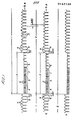
- Figure 1 of the drawings shows a typical example of a composite video signal (a frame signal) representing a frame, and including a field signal 1 representing an odd field in the composite video signal (the frame signal), and a field signal 2 representing an even field in the composite video signal (the frame signal).
- Reference numerals 3, 4, 5, 6, 7, 8 and 9 designate a vertical blanking period, front equalizing pulses, a vertical synchronizing signal, serrating pulses, back equalizing pulses, a horizontal synchronizing signal, and a video signal, respectively.
- FIG. 1 A portion A in Figure 1 is shown to an enlarged scale in Figure 2 of the drawings, in which reference numerals 10, 11, 12, 13 and 14 designate a horizontal blanking period, a front porch, a back porch, a pedestal level, and a sync tip level, respectively.
- the one-field/one-track recording method is classified into the so-called one-frame/two track recording method in which an odd field and an even field constituting a frame are sequentially recorded on two adjacent tracks respectively, and the so-called one-field recording method in which only one of an odd field and an even field only is recorded on one track.
- the so-called field/frame conversion mode is most frequently employed in which, utilizing the strong vertical correlation of horizontal scanning lines in a video signal, the same track is scanned twice to reproduce a frame signal from a field signal of one kind.
- This field/frame conversion mode is intended principally to improve the recording density so as to enable long-time recording in the case of a movie recording and to increase the number of pictures in the case of a still recording.
- the effect of interlaced scanning cannot be realized by merely repeatedly reproducing the same field signal twice.
- the converted frame signal includes a signal level difference and a pedestal level difference between the even and odd fields, resulting in appearance of flicker on the reproduced picture.
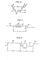
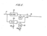
- this flicker preventing circuit includes an amplifier 2 0 , clamping circuits 21, 22, a gain-adjusting potentiometer VR 1 and a clamp-level adjusting potentiometer VR 2 associated with the combination of the 0.5H delay line 15 and the analog switch 16 of Figure 3.
- the gain of the amplifier 20 is adjusted by the gain-adjusting potentiometer VR 1 so that the converted frames signal has the same signal level in each field, and the clamping level is adjusted by the clamping-level adjusting potentiometer VR 2 so that the converted frame signal has the same pedestal level in each field.
- the above adjustment is usually made manually by the operator.
- the circuit of Figure 5 is unfit to meet the severe adjustment requirement of -40 dB or more demanded for preventing flicker, and is also unfit for mass production. Also, because the 0.5H delay line 15, analog switch 16, amplifier 20 and clamping circuits 21, 22 tend to undergo secular variations in addition to their inherent temperature dependencies, it has been impossible to completely eliminate the appearance of flicker attributable to the temperature dependences And secular variations of those parts, even when the appearance of flicker has been eliminated temporarily by adjustment of the potentiometers VR 1 and VR 2 .
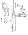
- FIG. 6 is a circuit diagram of the automatic flicker preventing circuit
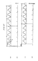
- Figure 7 illustrates the operation of various parts of the circuit of Figure 6.
- the automatic flicker preventing circuit includes a 0.5H delay line 15, a field-selecting analog switch 16, and an AGC loop 23 and a feedback-clamping loop 30.
- the AGC loop 23 acts to maintain constant the sync tip level (14 in Figure 2) and includes an automatic gain controller 24, the field-selecting analog switch 16, two input-selecting switches 25, 26, two peak detectors 27, 28, and a differential amplifier 29.
- the analog switch 16 presents a frame signal shown in Figure 7(a) as its output, and the input-selecting switches 25 and 26 are turned on/off as shown in Figures 7(c) and 7(d) respectively under control of a switch control pulse signal 35, which is shown in Figure 7(b) and selectively passed through an inverter 36. Consequently, the frame signal is applied to the peak detectors 27 and 28 at a time interval of IV as shown in Figures 7(e) and 7(f) respectively.
- the peak value of, for example, the even field signal detected by one of the peak detectors e.g.
- the peak detector 27, and the peak value of, for example, the odd field signal detected by the other peak detector 28, are applied to the differential amplifier 29, and the output signal 29a of the differential amplifier 29 indicative of the difference is applied to control the automatic gain controller 24 so as to attain coincidence of the peak values of the even and odd fields.
- the sync level and the signal level are maintained constant.
- the time constant selected is such that the AGC loop 23 responds to at least the unit field so that the signal level of a succeeding field signal becomes equal to that of a preceding field signal.
- the feedback-clamping loop 3Q acts to maintain constant the pedestal level (13 in Figure 2) and includes a sampling switch 31, an integrating circuit 32 and two clamping circuits 3 3, 34, besides the field selecting switch 16, Figure 7(g) shows the sampling timing of the sampling switch 31.
- the sampling switch 31 samples the pedestal level in each horizontal scanning period, and the integrating circuit 32 holds the sampled value and compares it with a reference value Vref 1 .
- the resultant difference signal 32a is applied from the integrating circuit 32 to the clamping circuits 33 and 34 each of which generates an output signal providing the pedestal level, so as to attain coincidence of the pedestal levels in the individual horizontal scanning periods.
- the time constant of this feedback-clamping loop 30 is selected to be lass than several H at the most so that the clamping level can be stabilized within the period of 1 H to 2H after change-over between the fields.
- flicker can be eliminated as early as possible even in the presence of variations in the characteristics of the two clamping circuits 33 and 34.
- Two capacitors 37 and 38 shown in Figure 6 are provided for the purpose of DC cut-off.
- the flicker preventing circuit described above the difference between the peak values (the sync tip levels) of an even field and an odd field is detected, and an automatic gain controller is controlled on the basis of the detected difference signal thereby maintaining constant the signal level in each of the fields.
- the pedestal level is sampled at a time interval of one horizontal scanning period (lH) to find the difference between the detected pedestal level and a reference value, and the clamping level is controlled on the basis of the detected difference signal thereby maintaining constant the pedestal level in each of the horizontal scanning periods.
- the pedestal level cannot be sampled in the vertical scanning period when a sampling pulse signal produced in synchronism with HD pulses derived from a synchronizing signal generator (SSG) is used for turning on/off the sampling switch 31. Accordingly, instead of making sampling of the pedestal level in the vertical scanning period, the voltage holding time of the integrating circuit 32 must be extended to about 4H so as to deal with the above situation. However, this leads to a problem of occurrence of a sag in the vertical scanning period and leads also to a problem of delayed response of the feedback-clamping loop. Further, there is the disadvantage that a synchronizing signal generator (SSG) and a sampling cancelling circuit are additionally required.
- SSG synchronizing signal generator
- the holding time of at least IV required for each of the peak detectors 27 and 28 has limited the response speed of the AGC loop, since these peak detectors 27 and 28 receive their input signals at a time interval of 1V only. Unless the AGC loop can respond sufficiently quickly, the AGC loop may not properly function in response to, for example, on/off of the power source or on/off of the input signal,
- the peak detectors 27 and 28 are provided independently of each other for detecting the peak values of the direct and delayed field signals respectively. Accordingly, when the temperature dependence of one of the peak detectors differs from that of the other, it leads to appearance of flicker although the flicker may not be very appreciable.
- a circuit for preventing flicker occurring on conversion of a field signal to a frame signal including delay means operative to delay a field signal supplied thereto by one half of a horizontal scanning period; a switching means operative to pass alternately the field signal directly or a delayed field signal from the delay means, the switching means being operated at a frequency of one vertical scanning period, and the output of the switching means being a frame signal; a feedback clamping loop comprising a sample and hold means sampling the pedestal level of the frame signal appearing at the output of the switching means, a clamping voltage generating means operative to compare the output signal from the sample and hold means with a reference value and generate a voltage signal proportional to the difference therebetween, and two clamping means connected to the direct and delayed field signal supply lines to the switching means respectively and controlled by the output signal from the clamping voltage generating means to maintain constant the pedestal level of the direct and delayed field signals, characterised by a synchronizing signal separating means operative to separate a synchronizing signal from the frame signal
- a circuit for preventing flicker occurring on conversion of a field signal to a frame signal including delay means operative to delay a field signal supplied thereto by one half of a horizontal scanning period; a switching means operative to pass alternately the field signal directly or a delayed field signal from the delay means, the switching means being operated at a frequency of one vertical scanning period, and the output of the switching means being a frame signal; a feedback clamping loop comprising a sample and hold means sampling the pedestal level of the frame signal appearing at the output of the switching means, a clamping voltage generating means operative to compare the output signal from the sample and hold means with a reference value and generate a voltage signal proportional to the difference therebetween, and two clamping means connected to the direct and delayed field signal supply lines to the switching means respectively and controlled by the output signal from - the clamping voltage generating means to maintain constant the pedestal level of the direct and delayed field signals, characterised by an automatic gain control loop comprising an automatic gain controller operative to amplify the frame signal
- a circuit for preventing flicker occurring on conversion of a field signal to a frame signal including delay means operative to delay a field signal supplied thereto by one half of a horizontal scanning period; a switching means operative to pass alternately the field signal directly or a delayed field signal from the delay means, the switching means being operated at a frequency of one vertical scanning period, and the output of the switching means being a frame signal; a feedback clamping loop comprising a sample and hold means sampling the pedestal level of the frame signal appearing at the output of the switching means, a clamping voltage generating means operative to compare the output signal from the sample -and hold means with a reference value and generate a voltage signal proportional to the difference therebetween, and two clamping means connected to the direct and delayed field signal supply lines to the switching means respectively and controlled by the output signal from the clamping voltage generating means to maintain constant the pedestal level of the direct and delayed field signals, characterised by an automatic gain control loop comprising an automatic gain controller connected in either the direct field signal line
- the embodiment of the present invention here shown comprises a 0.5H delay line 15, a change-over switch 16, an automatic gain controller 24, clamping circuits 33 and 34, DC cut-off capacitors 37 and 38, impedance-converting emitter follower circuits 39 to 43, an AGC loop 44, and a feedback-clamping loop 45.
- Reference numerals 17 and 18 designate a direct field signal and a 0.5H delayed field signal respectively.
- the feedback-clamping loop 45 includes a synchronizing signal,separating means 50 operative to separate a synchronizing signal 50a from a frame signal 46 appearing from the switch 16, a sampling pulse generating means 52 operative to produce a sampling pulse signal 52a on the basis of the separated synchronizing signal 50a, a sample and hold means 53 operative to sample the pedestal level of the frame signal 46 in response to the sampling pulse signal 52a, a clamping voltage generating means 54 operative to compare the output signal 53a of the sample and hold means 53 With a reference value Vref 1 And generate a voltage signal 54a proportional to the difference therebetween, and two clamping circuits 33 and 34 connected to the delayed and direct field signal lines 18 and 17, respectively.
- the waveform of the separated synchronizing signal 50a is shown in Figure 9(a), and that of the sampling pulse signal 52a is shown in Figure 9(b).
- the sampling pulse signal 52a is synchronous with the rising edges of the pulses of the synchronizing signal 50a, that is, synchronous with the change points from the sync tip level to the pedestal level of the signal 50a, and the pulse width of the signal 52a is equal to or smaller than that of the serrating pulses 6 appearing in the vertical synchronizing period 5 ( Figure 1). Therefore, the sample and hold means 53 can detect the pedestal level during the entire period including the vertical blanking period 3 ( Figure 1) of the frame signal 46.
- the clamping voltage generating means 54 compares the sampled pedestal level with the reference value Vref 1 and applies its output.signal 54a indicative of the difference therebetween to the clamping means 33 and 34 so that the direct and delayed field signals 17 and 18 have the same And constant pedestal level, Therefore, the feedback-clamping loop 45 can clamp the pedestal level during the entire period including the vertical blanking period. Also, since the sampling interval is not longer than 1H, the required voltage holding time of the sample and hold means 53 is as short as only about lH, so that the feedback-clamping loop 45 can respond quickly.
- the sampling pulse signal 52a for sampling the pedestal level is produced on the basis of the synchronizing signal 50a separated from the frame signal 46.
- the pedestal level can be sampled even in the vertical synchronizing period. Therefore, the feedback-clamping on the basis of the sampled pedestal level eliminates an undesirable sag appearing in the vertical synchronizing period.
- the voltage holding time of the sample and hold means 53 is short or only about 1H, the clamping operation is done with a good response performance regardless of on/off of the power source or position of the switch 16.
- no special unit such as a synchronizing signal generator (SSG) for producing horizontal synchronizing pulses (HD pulses) is necessary.
- SSG synchronizing signal generator
- This AGC loop 44 includes the automatic gain controller 24 operative to amplify the frame signal 46 applied-from the switch 16, a sample and hold means 48 operative to sample the peak, that is, the sync tip level of the amplified frame signal 47, a gain-control voltage generating means 49 operative to compare the output signal 48a of the sample and hold means 48 with a reference value Vref 2 and generate a voltage signal 49a proportional to the difference therebetween, the synchronizing signal separating means 50 operating to separate-the synchronizing signal 50a from the frame signal 46, and a sampling pulse generating means 51 operative to produce a sampling pulse signal 51a on the basis of the separated synchconizing signal 50a.
- This sampling pulse signal 51a has a waveform as shown in Figure 9(c). It will be seen in Figure 9(c) that the sampling pulse signal 51a is synchronous with the falling edges, that is, the change points from the pedestal level to the sync tip level of the synchronizing signal 50a, and its pulse width is equal to or smaller than that of the serrations of the sync level or equalizing pulses in the equalizing periods 4 and 7 ( Figure 1). Therefore, the sample and hold means 48 can detect the sync tip level during the entire period including the vertical blanking period 3( Figure 1) of the amplified frame signal 47. Thus, the sample and hold means 48 operates as a peak detector.
- the gain-control voltage generating means 49 compares the output signal 48a of the sample and hold means 48 with the reference value Vref 2 , and applies a voltage signal 49a indicative of the difference therebetween to the automatic gain controller 24, so that the sync tip level of the amplified frame signal 47 can be maintained constant. Therefore, the required voltage holding time of the sample and hold means 48 is short or only about 1H, so that the AGC loop 44 can respond very quickly. Thus, the AGC loop 44 makes its AGC operation immediately in response to on/off of the power source or operation of the switch 16.
- the AGC loop 23 in the known flicker preventing circuit shown in Figure 6 includes two peak detectors 27 and 28, and a difference between the temperature dependencies of these two peak detectors 27 and 28 can result in the appearance of flicker.
- the AGC loop 44 in ,n the circuit shown in Figure 8 includes only one peak detector, Thus, no flicker attributable to the temperature dependence of the single peak detector appears.
- the embodiment of the invention shown-in Figure 10 is a modification of the embodiment shown in Figure 8 in that its AGC loop 55 only is slightly different from the AGC loop 44 shown in Figure .8.
- the AGC loop 55 includes a peak detector 56 combined with the automatic gain controller 24 and the gain-control voltage generating means 49.
- the sampling pulse generating means 51 shown in Figure 8 is eliminated.
- the peak detector 56 detects the peak value, that is, the sync tip level of the amplified frame signal 47.
- the voltage holding time is selected to be about 1H
- the AGC loop 55 can respond very quickly as in the case of the embodiment shown in Figure 8. Further, since only one peak detector 56 is provided for the peak detection, no flicker atributable to the temperature dependence of the single peak detector 56 appears.
- the frame signal 46 obtained by conversion of the direct and delayed field signals 17 and 18 by the switch 16 is amplified by the automatic gain controller 24, and the peak value (the sync tip level) of the amplified frame signal 47 is detected by the peak detecting circuit 48 or 56 to be compared with the reference value Vref 2 .
- the automatic gain controller 24 is so controlled that the peak value of the amplified frame signal 47 can be maintaned constant. Therefore, only one peak detecting circuit suffices, and there is always an input applied thereto.
- the input signal is always applied to the peak detecting circuit, the voltage holding time which is as short as about 1H, suffices, and the AGC loop can respond very quickly. Also, since only one peak detecting circuit is provided, no flicker attributable to the temperature dependence of the single peak detecting circuit appears.
- the feedback-clamping loop 45 shown in each of Figures 8 and lO may be replaced by that 30 shown in Figure 6. In such a case, however, it is a general procedure that a sampling pulse signal is produced on the basis of HD pulses from a synchronizing signal generator (SSG) and is applied to the sampling switch 31.
- SSG synchronizing signal generator
- the feedback-clamping loop 45 shown in each of Figures 8 and 10 is advantageous over the loop 30 shown in Figure 6 in that the capability of clamping of the pedestal level even in the vertical synchronizing period eliminates occurrence of an undesirable sag, and the quick response ensures immediate starting of the clamping operation in response to on/off of the power source or operation of the switch 16.
- the flicker preventing circuit shown in Figure 11 is an improvement in the known circuit shown in Figure 6.
- the structure shown in Figure 11 is the same as that shown in Figure 6 except that two peak detectors 58 and 59 each having a voltage holding time of about 1H are disposed in a stage preceding the switch 16, and the clamped signal from the clamping circuits 33 and 34 is directly applied to the peak detectors 58 and 59 respectively to constitute an AGC loop 57.
- emitter follower circuits 60 and 61 are provided for the purpose of impedance conversion.
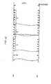
- the field signal 18 passed through the 0.5H delay line 15 is applied to one of the peak detectors, e.g. peak detector 58 ( Figure 12(c)), and, at the same time, the direct field signal 17 is applied to the other peak detector 59 ( Figure 12(a) ).
- the two peak detectors 58 and 59 detect the peak values, that is, the sync tip levels of the respective field signals at a time interval of 1H, and their output signals indicative of the detected sync tip levels (Figs. 12(d) and 12 (b) ) respectively are applied to the differential amplifier 29.
- the differential amplifier 29 applies its output signal 29a, proportional to the difference between the two inputs, to the automatic gain controller 24 to control the gain so that coincidence can be achieved between the sync tip levels of the direct field signal 17 and the delayed field signal 18.
- the voltage holding time required for each of the peak detectors 58 and 59 is as short as about 1H, since they always have inputs thereto unlike those shown in Figure 6. Therefore, the AGC loop 57 can respond very quickly.
- the feedback-clamping loop 30 in Figure 11 is the same as that 30 shown in Figure 6. In the loop 30, the pedestal level of the frame signal 62 sampled by the sampling switch 31 is held in the integrating circuit 32 and also compared with the reference value Vref 1 . The clamping potential signal 32a proportional to the difference therebetween is applied from the integrating circuit 32 to the clamping means 33 and 34 to control the latter, thereby maintaining constant the pedestal level.
- the peak detectors 58 and 59 in Figure 11 may be either peak detecting means or sample and hold means. However, it is necessary to set the detection timing so that the sync tip level of each field signal can be detected in a manner as shown in Figure 12.
- Figure 13 shows an embodiment which includes a modified feedback-clamping loop designated generally by the reference numeral 63.
- the AGC loop 57 is-the same as that shown in Figure 11.
- the feedback-clamping loop 63 in the embodiment shown in Figure 13 is improved in its response speed compared with the loops 30 shown in Figures 6 and 11, and reduces the possibility of a sag which may occur during the vertical synchronizing period 5 ( Figure 1).
- the sampling switch 31 is actuated by a sampling pulse signal produced on the basis of HD pulses from a synchronizing signal generator (SSG). Therefore, as previously described, it is normally unable to sample the pedestal level during the vertical synchronizing period 5, and it becomes necessary to extend the voltage holding time of the integrating circuit 32 to a considerably long period of about 4H.
- SSG synchronizing signal generator
- the feedback-clamping loop 63 in the embodiment shown in Figure 13 includes a synchronizing signal separating means 64 operative to separate the synchronizing signal 64a from the frame signal 62 obtained from the switch 16, a sampling pulse generating means 65 operative to produce a sampling pulse signal 65a on the basis of the separated synchronizing signal 64a, a sample and hold means 66 operative to sample the pedestal level of the frame signal 62 in response to the sampling pulse signal 65a, a clamping voltage generating means 67 operative to compare the output signal 66a of the sample and hold means 66 with a reference value Vref 1 and generate a voltage signal 67a proportional to the difference therebetween, and the aforementioned two clamping means 33 and 34 connected to the delayed and direct field signal lines 18 and 17, respectively.
- the waveform of the separated synchronizing signal 64a is shown in Figure 14(a), and that of the sampling pulse signal 65a is shown in Figure 14(b). It will be seen in Figure 14(b) that the sampling pulse signal 65a is synchronous with the rising edges of the pulses, that is, the change points from the sync tip level to the pedestal level of the synchronizing signal 64a, and the pulse width of the signal 65a is equal to or smaller than that of the serrating pulses 6 appearing in the vertical synchronizing period 5 ( Figure 1). Therefore, the sample and hold means 66 can detect the pedestal level during the entire period including the vertical blanking period 3 ( Figure 1) of the frame signal 62.
- the clamping voltage generating means 67 compares the sampled pedestal level with the reference valve Vref 1 and applies its output signal 67a indicative of the difference therebetween to the clamping means 33 and 34 so that the direct and delayed field signals 17 and 18 have the same and constant pedestal level. Therefore, the feedback-clamping loop 63 can clamp the pedestal level during the entire period including the vertical blanking period. Also, since the sampling interval is not longer than 1H, the required voltage holding time of the sample and hold circuit 66 is as short as only about 1H, so that the feedback-clamping loop 63 can operate with a high response speed.
- the automatic gain controller 24 is inserted in the same signal line as the 0.5H delay line 15 in the embodiments shown in Figures 11 and 13, it may otherwise be inserted in the direct field signal line, In such a case, it is preferable that the peak detectors 58 and 59 are connected to the plus and minus input terminals respectively of the differential amplifier 29 as shown in Figure 15, unlike the connections shown in Figures 11 and 13.
- the peak values of the direct field signal and delayed field signal respectively are detected before being converted into the frame signal. Therefore, the two peak detecting circuits 58 and 59 always have input signals applied thereto, and the voltage holding time is as short as about 1H, so that the AGC loop can make the AGC operation with a very high response speed. It is apparent that the frame signal after conversion can be automatically controlled to have the same signal level between the fields, because the automatic gain controller 24 is controlled by the difference signal indicative of the difference between the peak values of the-direct and delayed field signals.
- the pedestal level of the frame signal can be automatically maintained constant, because the pedestal level of the fieldframe converted signal is sampled at the time interval of one horizontal scanning period (lH) so as to control the clamping level of the direct and delayed field signals before being converted into the frame signal. Therefore, even in the presence of temperature dependencies and/or secular variations in the components of the field signal/frame signal conversion circuit, appearance of flicker can be minimized. Also, by virtue of the fact that the signal level and pedestal level can be automatically adjusted, the manual adjustment required hitherto during the manufacturing process is unnecessary, and the flicker preventing circuit is suitable for mass-production.
Landscapes
- Engineering & Computer Science (AREA)
- Multimedia (AREA)
- Signal Processing (AREA)
- Television Systems (AREA)
Applications Claiming Priority (6)
| Application Number | Priority Date | Filing Date | Title |
|---|---|---|---|
| JP58233483A JPS60126982A (ja) | 1983-12-13 | 1983-12-13 | フイ−ルド信号・フレ−ム信号変換におけるフリツカ防止回路 |
| JP58233481A JPS60126980A (ja) | 1983-12-13 | 1983-12-13 | フイ−ルド信号・フレ−ム信号変換におけるフイ−ドバツク・クランプ回路 |
| JP233481/83 | 1983-12-13 | ||
| JP58233482A JPS60126981A (ja) | 1983-12-13 | 1983-12-13 | フイ−ルド信号・フレ−ム信号変換におけるフリツカ防止回路 |
| JP233483/83 | 1983-12-13 | ||
| JP233482/83 | 1983-12-13 |
Publications (3)
| Publication Number | Publication Date |
|---|---|
| EP0147138A2 true EP0147138A2 (de) | 1985-07-03 |
| EP0147138A3 EP0147138A3 (en) | 1986-02-19 |
| EP0147138B1 EP0147138B1 (de) | 1989-03-08 |
Family
ID=27332002
Family Applications (1)
| Application Number | Title | Priority Date | Filing Date |
|---|---|---|---|
| EP84308709A Expired EP0147138B1 (de) | 1983-12-13 | 1984-12-13 | Schaltung zur Verhinderung von Flimmern |
Country Status (3)
| Country | Link |
|---|---|
| US (1) | US4626910A (de) |
| EP (1) | EP0147138B1 (de) |
| DE (1) | DE3477120D1 (de) |
Cited By (1)
| Publication number | Priority date | Publication date | Assignee | Title |
|---|---|---|---|---|
| US4816907A (en) * | 1986-04-25 | 1989-03-28 | U.S. Philips Corporation | Television synchronizing signal pattern correction circuit |
Families Citing this family (7)
| Publication number | Priority date | Publication date | Assignee | Title |
|---|---|---|---|---|
| JP2573925B2 (ja) * | 1985-07-16 | 1997-01-22 | 富士写真フイルム株式会社 | 画像ハ−ドコピ−作成装置 |
| JPS6218881A (ja) * | 1985-07-18 | 1987-01-27 | Fuji Photo Film Co Ltd | フイ−ルド/フレ−ム変換方式 |
| US5428456A (en) * | 1991-03-15 | 1995-06-27 | Eastman Kodak Company | Method and apparatus for adaptively reducing interline flicker of TV-displayed image |
| GB9307681D0 (en) * | 1993-04-14 | 1993-06-02 | Rca Thomson Licensing Corp | Line flicker suppression system |
| US5627555A (en) * | 1993-04-14 | 1997-05-06 | Rca Thomson Licensing Corporation | Line flicker suppression by adaptive de-interlacing |
| JPH07131677A (ja) * | 1993-11-02 | 1995-05-19 | Nec Corp | ビデオ信号のサグ補正回路 |
| KR0152049B1 (ko) * | 1995-08-03 | 1998-10-15 | 김광호 | 디지탈 변조시스템의 제어신호 부가장치 |
Citations (1)
| Publication number | Priority date | Publication date | Assignee | Title |
|---|---|---|---|---|
| JPS58189202A (ja) | 1982-04-30 | 1983-11-04 | Denki Kagaku Kogyo Kk | 微粒子状クロロプレン重合体凝固物の製造方法 |
Family Cites Families (9)
| Publication number | Priority date | Publication date | Assignee | Title |
|---|---|---|---|---|
| US3886589A (en) * | 1972-09-13 | 1975-05-27 | Matsushita Electric Industrial Co Ltd | Video recording system for reducing flicker in the skip field mode |
| NL7511784A (nl) * | 1975-03-24 | 1977-04-13 | Philips Nv | Werkwijze en inrichting voor het maken van een videoplaat. |
| US4121250A (en) * | 1976-07-26 | 1978-10-17 | Hughes Aircraft Company | Flicker free scan conversion system |
| DE2640759C2 (de) * | 1976-09-10 | 1982-10-14 | Robert Bosch Gmbh, 7000 Stuttgart | System zur Wiedergabe von Videosignalen |
| JPS5437528A (en) * | 1977-08-30 | 1979-03-20 | Sony Corp | Processing circuit for video signal |
| US4213151A (en) * | 1978-08-18 | 1980-07-15 | Rca Corporation | AGC keying signal circuit |
| JPS5552506A (en) * | 1978-10-05 | 1980-04-17 | Toshiba Corp | Agc circuit of vtr |
| JPS5745782A (en) * | 1980-09-02 | 1982-03-15 | Sony Corp | Flicker preventing circuit |
| US4386367A (en) * | 1981-06-26 | 1983-05-31 | Tektronix, Inc. | System and method for converting a non-interlaced video signal into an interlaced video signal |
-
1984
- 1984-12-11 US US06/680,654 patent/US4626910A/en not_active Expired - Lifetime
- 1984-12-13 EP EP84308709A patent/EP0147138B1/de not_active Expired
- 1984-12-13 DE DE8484308709T patent/DE3477120D1/de not_active Expired
Patent Citations (1)
| Publication number | Priority date | Publication date | Assignee | Title |
|---|---|---|---|---|
| JPS58189202A (ja) | 1982-04-30 | 1983-11-04 | Denki Kagaku Kogyo Kk | 微粒子状クロロプレン重合体凝固物の製造方法 |
Cited By (1)
| Publication number | Priority date | Publication date | Assignee | Title |
|---|---|---|---|---|
| US4816907A (en) * | 1986-04-25 | 1989-03-28 | U.S. Philips Corporation | Television synchronizing signal pattern correction circuit |
Also Published As
| Publication number | Publication date |
|---|---|
| DE3477120D1 (en) | 1989-04-13 |
| EP0147138B1 (de) | 1989-03-08 |
| US4626910A (en) | 1986-12-02 |
| EP0147138A3 (en) | 1986-02-19 |
Similar Documents
| Publication | Publication Date | Title |
|---|---|---|
| EP0133049B1 (de) | Gerät zur Aufzeichnung und Wiedergabe von Fernsehsignalen | |
| GB2079090A (en) | Variable aspect ratio television receivers | |
| JP2760809B2 (ja) | テレビジョン受信機 | |
| JPH0320957B2 (de) | ||
| US5057923A (en) | Image pickup device capable of picking up images while electronically enlarging the same | |
| JPS60160290A (ja) | ビデオ信号記録再生装置 | |
| EP0147138B1 (de) | Schaltung zur Verhinderung von Flimmern | |
| US4581642A (en) | Televison noise reduction system for a signal source having variable picture repetition | |
| EP0041868B1 (de) | Anordnung zur Verarbeitung von Videosignalen | |
| CA1070831A (en) | Apparatus for reading a record of disc form | |
| EP0278733B1 (de) | Vorrichtung für die Aufnahme und Wiedergabe eines Videosignals | |
| US4459620A (en) | Color video signal reproducing apparatus | |
| JPH0478070B2 (de) | ||
| JPH0478072B2 (de) | ||
| US4758900A (en) | Field/frame conversion method for magnetic picture recording with demodulation, interpolation and de-emphasis after conversion | |
| JPH0478071B2 (de) | ||
| JPH0451118B2 (de) | ||
| JPH055236B2 (de) | ||
| EP0196097A2 (de) | Verfahren zur Raster/Bildkonvertierung in der magnetischen Bildaufzeichnung und -wiedergabe | |
| EP0479135B1 (de) | Vorrichtung zum Verarbeiten eines Bildsignals | |
| JPH0554760B2 (de) | ||
| KR890004227B1 (ko) | 색신호 처리장치 | |
| JPH05316468A (ja) | ノイズリデューサ | |
| EP0296831A1 (de) | Spannungsgeregeltes Kammfilter | |
| JP2754545B2 (ja) | ドロップアウト補償回路 |
Legal Events
| Date | Code | Title | Description |
|---|---|---|---|
| PUAI | Public reference made under article 153(3) epc to a published international application that has entered the european phase |
Free format text: ORIGINAL CODE: 0009012 |
|
| AK | Designated contracting states |
Designated state(s): DE FR GB NL |
|
| PUAL | Search report despatched |
Free format text: ORIGINAL CODE: 0009013 |
|
| RHK1 | Main classification (correction) |
Ipc: H04N 5/21 |
|
| AK | Designated contracting states |
Designated state(s): DE FR GB NL |
|
| 17P | Request for examination filed |
Effective date: 19860816 |
|
| 17Q | First examination report despatched |
Effective date: 19880407 |
|
| GRAA | (expected) grant |
Free format text: ORIGINAL CODE: 0009210 |
|
| AK | Designated contracting states |
Kind code of ref document: B1 Designated state(s): DE FR GB NL |
|
| REF | Corresponds to: |
Ref document number: 3477120 Country of ref document: DE Date of ref document: 19890413 |
|
| ET | Fr: translation filed | ||
| PLBE | No opposition filed within time limit |
Free format text: ORIGINAL CODE: 0009261 |
|
| STAA | Information on the status of an ep patent application or granted ep patent |
Free format text: STATUS: NO OPPOSITION FILED WITHIN TIME LIMIT |
|
| 26N | No opposition filed | ||
| REG | Reference to a national code |
Ref country code: GB Ref legal event code: IF02 |
|
| PGFP | Annual fee paid to national office [announced via postgrant information from national office to epo] |
Ref country code: FR Payment date: 20031125 Year of fee payment: 20 |
|
| PGFP | Annual fee paid to national office [announced via postgrant information from national office to epo] |
Ref country code: GB Payment date: 20031209 Year of fee payment: 20 |
|
| PGFP | Annual fee paid to national office [announced via postgrant information from national office to epo] |
Ref country code: NL Payment date: 20031215 Year of fee payment: 20 |
|
| PGFP | Annual fee paid to national office [announced via postgrant information from national office to epo] |
Ref country code: DE Payment date: 20040130 Year of fee payment: 20 |
|
| PG25 | Lapsed in a contracting state [announced via postgrant information from national office to epo] |
Ref country code: GB Free format text: LAPSE BECAUSE OF EXPIRATION OF PROTECTION Effective date: 20041212 |
|
| PG25 | Lapsed in a contracting state [announced via postgrant information from national office to epo] |
Ref country code: NL Free format text: LAPSE BECAUSE OF EXPIRATION OF PROTECTION Effective date: 20041213 |
|
| REG | Reference to a national code |
Ref country code: GB Ref legal event code: PE20 |
|
| NLV7 | Nl: ceased due to reaching the maximum lifetime of a patent |
Effective date: 20041213 |