EP0143496B1 - Blooming-insensitive image sensor device and method of manufacturing same - Google Patents
Blooming-insensitive image sensor device and method of manufacturing same Download PDFInfo
- Publication number
- EP0143496B1 EP0143496B1 EP84201684A EP84201684A EP0143496B1 EP 0143496 B1 EP0143496 B1 EP 0143496B1 EP 84201684 A EP84201684 A EP 84201684A EP 84201684 A EP84201684 A EP 84201684A EP 0143496 B1 EP0143496 B1 EP 0143496B1
- Authority
- EP
- European Patent Office
- Prior art keywords
- channel regions
- conductivity type
- image sensor
- sensor device
- zones
- Prior art date
- Legal status (The legal status is an assumption and is not a legal conclusion. Google has not performed a legal analysis and makes no representation as to the accuracy of the status listed.)
- Expired
Links
- 238000004519 manufacturing process Methods 0.000 title claims abstract description 9
- 239000004065 semiconductor Substances 0.000 claims abstract description 64
- 239000000758 substrate Substances 0.000 claims abstract description 37
- 238000000926 separation method Methods 0.000 claims abstract description 25
- 238000009792 diffusion process Methods 0.000 claims description 16
- 230000000873 masking effect Effects 0.000 claims description 16
- 230000005855 radiation Effects 0.000 claims description 11
- 239000012535 impurity Substances 0.000 claims description 8
- 238000000034 method Methods 0.000 claims description 5
- 108091006146 Channels Proteins 0.000 description 91
- 238000005036 potential barrier Methods 0.000 description 13
- 230000010354 integration Effects 0.000 description 11
- 239000000463 material Substances 0.000 description 6
- 230000015572 biosynthetic process Effects 0.000 description 5
- 230000035945 sensitivity Effects 0.000 description 5
- VYPSYNLAJGMNEJ-UHFFFAOYSA-N Silicium dioxide Chemical compound O=[Si]=O VYPSYNLAJGMNEJ-UHFFFAOYSA-N 0.000 description 3
- 229910052814 silicon oxide Inorganic materials 0.000 description 3
- XUIMIQQOPSSXEZ-UHFFFAOYSA-N Silicon Chemical compound [Si] XUIMIQQOPSSXEZ-UHFFFAOYSA-N 0.000 description 2
- 229910052710 silicon Inorganic materials 0.000 description 2
- 239000010703 silicon Substances 0.000 description 2
- 230000003595 spectral effect Effects 0.000 description 2
- 102000004129 N-Type Calcium Channels Human genes 0.000 description 1
- 108090000699 N-Type Calcium Channels Proteins 0.000 description 1
- XAGFODPZIPBFFR-UHFFFAOYSA-N aluminium Chemical compound [Al] XAGFODPZIPBFFR-UHFFFAOYSA-N 0.000 description 1
- 229910052782 aluminium Inorganic materials 0.000 description 1
- 239000004411 aluminium Substances 0.000 description 1
- 238000010276 construction Methods 0.000 description 1
- 239000002019 doping agent Substances 0.000 description 1
Images

Classifications
-
- H—ELECTRICITY
- H01—ELECTRIC ELEMENTS
- H01L—SEMICONDUCTOR DEVICES NOT COVERED BY CLASS H10
- H01L29/00—Semiconductor devices adapted for rectifying, amplifying, oscillating or switching, or capacitors or resistors with at least one potential-jump barrier or surface barrier, e.g. PN junction depletion layer or carrier concentration layer; Details of semiconductor bodies or of electrodes thereof ; Multistep manufacturing processes therefor
- H01L29/66—Types of semiconductor device ; Multistep manufacturing processes therefor
- H01L29/68—Types of semiconductor device ; Multistep manufacturing processes therefor controllable by only the electric current supplied, or only the electric potential applied, to an electrode which does not carry the current to be rectified, amplified or switched
- H01L29/76—Unipolar devices, e.g. field effect transistors
-
- H—ELECTRICITY
- H01—ELECTRIC ELEMENTS
- H01L—SEMICONDUCTOR DEVICES NOT COVERED BY CLASS H10
- H01L27/00—Devices consisting of a plurality of semiconductor or other solid-state components formed in or on a common substrate
- H01L27/14—Devices consisting of a plurality of semiconductor or other solid-state components formed in or on a common substrate including semiconductor components sensitive to infrared radiation, light, electromagnetic radiation of shorter wavelength or corpuscular radiation and specially adapted either for the conversion of the energy of such radiation into electrical energy or for the control of electrical energy by such radiation
- H01L27/144—Devices controlled by radiation
- H01L27/146—Imager structures
- H01L27/148—Charge coupled imagers
- H01L27/14887—Blooming suppression
-
- H—ELECTRICITY
- H01—ELECTRIC ELEMENTS
- H01L—SEMICONDUCTOR DEVICES NOT COVERED BY CLASS H10
- H01L27/00—Devices consisting of a plurality of semiconductor or other solid-state components formed in or on a common substrate
- H01L27/14—Devices consisting of a plurality of semiconductor or other solid-state components formed in or on a common substrate including semiconductor components sensitive to infrared radiation, light, electromagnetic radiation of shorter wavelength or corpuscular radiation and specially adapted either for the conversion of the energy of such radiation into electrical energy or for the control of electrical energy by such radiation
- H01L27/144—Devices controlled by radiation
- H01L27/146—Imager structures
- H01L27/148—Charge coupled imagers
- H01L27/14831—Area CCD imagers
-
- Y—GENERAL TAGGING OF NEW TECHNOLOGICAL DEVELOPMENTS; GENERAL TAGGING OF CROSS-SECTIONAL TECHNOLOGIES SPANNING OVER SEVERAL SECTIONS OF THE IPC; TECHNICAL SUBJECTS COVERED BY FORMER USPC CROSS-REFERENCE ART COLLECTIONS [XRACs] AND DIGESTS
- Y10—TECHNICAL SUBJECTS COVERED BY FORMER USPC
- Y10S—TECHNICAL SUBJECTS COVERED BY FORMER USPC CROSS-REFERENCE ART COLLECTIONS [XRACs] AND DIGESTS
- Y10S438/00—Semiconductor device manufacturing: process
- Y10S438/965—Shaped junction formation
Definitions
- the invention relates to an image sensor device comprising a semiconductor substrate of a first conductivity type having a number of surface-adjoining channel regions of the first conductivity type which are directed at right angles to a system of electrodes present on and insulated from the surface, in which during operation charge produced by incident radiation is collected and transported and which are mutually separated by surface-adjoining channel separation zones of the second opposite conductivity type and further adjoin a semiconductor zone of the second conductivity type extending substantially parallel to the surface, the channel regions having a dopant concentration which exceeds that of the semiconductor zone, which in turn exceeds the doping concentration of the semiconductor substrate.
- the invention further relates to a method of manufacturing such a device.
- the application of suitable voltages between the electrodes, the semiconductor zone and the substrate will result in a potential variation between the surface and the substrate which exhibits a potential barrier at the area of the semiconductor zone.
- charge which, viewed from the surface, is produced above this potential barrier in the semiconductor material will contribute to the formation of the charge image, whereas charge produced beneath this potential barrier will not contribute to the formation of the charge image.
- the spectral sensitivity of the image sensor device is determined by the position of the potential barrier.
- GB-A-2054961 discloses an image sensor device of the kind mentioned in the opening paragraph in which the channel regions have a doping concentration which does not exceed that of the semiconductor zone and the substrate.
- charge collected in the channel regions can influence the potential variation between the surface and the semiconductor substrate in such a manner that the potential barrier, which was initially present at the area of the semiconductor zone, disappears when a given quantity of charge is exceeded during the integration period.
- the excess of charge can flow away to the semiconductor substrate.
- This phenomenon often designated as "blooming" can give rise to very disturbing lines in a television picture, which is formed by means of signals obtained with such an image sensor device.
- the known image sensor device comprises a semiconductor substrate on which two semiconductor layers are disposed of which the upper layer comprises the channel regions having a doping concentration which does not exceed that of the semiconductor substrate.
- Such a construction cannot be obtained by means of diffusion of impurities in semiconductor materials.
- a zone of the other conductivity type can be formed whose doping concentration exceeds that of the semiconductor body.
- a layer of the first conductivity type will have to be grown epitaxially onto a semiconductor substrate. In this layer structure, channel separation zones extending into the semiconductor zone can be formed by means of diffusion of impurities in both layers.
- the channel regions have a width which is determined during the manufacture of the channel separation zones. This zones will have a minimum width which is equal to the minimum dimensions of a window required for the diffusion, plus on both sides the distance over which lateral diffusion takes place. This distance is larger in the known image sensor device than the thickness of the layer in which the channel regions are formed. Starting from a desired centre distance between adjacent channel regions, the desired centre distance minus the width of the required diffusion window and well over twice the thickness of the channel regions is then left for the width of the channel regions. In practice, the desired centre distance is, for example, 10 pm, the width of the window is 4 pm and the thickness of the channel regions is 1 Ilm; for the width of the channel regions only about 3 ⁇ m is left.
- the known image sensor device consequently has comparatively narrow channel regions and comparatively wide channel separation zones. This is an undesirable situation because thus not only the quantity of charge that can be collected and transported per unit surface area is comparatively small, but also the image sensor device consequently has a comparatively low sensitivity. Charge produced in the channel separation zones can flow away to the semiconductor substrate and will then not contribute to the image formation.
- the invention has inter alia for its object to provide an image sensor device of the kind mentioned in the opening paragraph, in which charge collected in the channel regions also can influence the potential variation between the surface and the semiconductor substrate in such a manner that an excess of charge can flow away to the semiconductor substrate and which has comparatively wide channel regions and comparatively narrow channel separation zones.
- the image sensor device of the kind mentioned in the opening paragraph in accordance with the invention is characterized in that the semiconductor zone has a thickness which varies in the direction at right angles to the channel regions, the thickness housing minima at the centres of the channel regions.
- the image sensor device can be manufactured in a simple manner by means of diffusion of impurities in a semiconductor substrate of the first conductivity type.
- zones of the second conductivity type can be provided by means of a first masking with windows extending at a fixed relative centre distance and then zones of the first conductivity type forming the channel regions can be provided by means of a second masking with windows extending at the same relative centre distance.
- the second masking is then arranged so that the channel regions are formed halfway between the zones of the second conductivity type.
- the channel regions are then mutually separated by surface-adjoining zones of the second conductivity type (the channel separation zones), while they further adjoin a zone of the second conductivity type extending substantially parallel to the surface.
- This zone has a thickness, which extends in a direction at right angles to the channel regions and has minima at the centres of the channel regions.
- the channel regions have a doping concentration which exceeds that of the subjacent semiconductor zone, while the latter in turn has a doping concentration which exceeds that of the semiconductor substrate. As a result, an effective anti-blooming is possible.
- the width of the channel regions is equal to the width of the windows in the second masking plus the distance over which lateral diffusion takes place. This distance is substantially equal to the thickness of the channel regions. In this case a limiting factor is the minimum distance which has to be observed between two windows. With a desired centre distance between the channel regions, the maximum width of these channel regions is equal to this centre distance minus the minimum window distance and plus twice the thickness of the channel regions. In a practical embodiment corresponding to the foregoing, the centre distance is 10 pm, the minimum window width is 4 pm and the thickness of the channel regions is 1 um; the width of the channel regions then becomes at least 8 pm. As compared with the known image sensor device, the image sensor device according to the invention has comparatively wide channel regions and comparatively narrow channel separation zones.
- the invention further relates to a method of manufacturing an image sensor device of the kind mentioned in the opening paragraph.
- This method is characterized in that zones of the second conductivity type are provided in a semiconductor substrate of the first conductivity type by means of diffusion of impurities through a first masking with windows extending at a fixed relative centre distance and then zones of the first conductivity type forming the channel regions are provided through a second masking with windows extending at the same relative centre distance, the second masking being arranged so that the channel regions are formed halfway between the zones of the second conductivity type.
- an image sensor device in which the channel regions are mutually separated by surface-adjoining semiconductor zones of the second conductivity type (the channel separation zones) and which further adjoin a semiconductor zone of the second conductivity type.
- the channel regions have a 'doping concentration which exceeds that of the semiconductor zone, which in turn has a doping concentration which exceeds that of the semiconductor substrate.
- the semiconductor zone has a thickness which has in the direction at right angles to the channel regions a variation with minima at the centres of the channel regions.
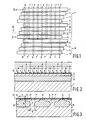
- Figures 1 to 3 show diagrammatically an image, sensor device comprising a semiconductor substrate 1 of a first conductivity type, in the example an n-type silicon substrate.
- a surface 2 thereof is adjoined by a number of channel regions 7 of the first conductivity type which are directed at right angles to a system of electrodes 3, 4, 5 and 6 present on the surface, in which during operation charge is collected and transported and which are mutually separated by channel separation zones 8 of the second opposite conductivity type adjoining the surface 2 and which further adjoin a semiconductor zone 9 of the second conductivity type extending substantially parallel to the surface 2.
- the electrodes 3,4, 5 and 6 are insulated from the surface 2 by an insulating layer 10 of, for example, silicon oxide.
- clock pulses are applied to the electrodes 3, 4, 5 and 6 and to electrodes 12, 13, 14 and 15, as a result of which the collected charge packets are transported through the channel regions 7 and are transferred, for example, to a storage register 16,
- the charge can then be read from this register during a next integration time for further signal processing.
- the storage register 16 is covered by a reflecting aluminium layer not shown so that the charge in this register cannot be modified by incident radiation.
- the channel regions 7 have a doping concentration which exceeds that of the semiconductor zone 9,which in turn exceeds that of the substrate 1.
- the doping concentration of the n-type channel regions is about 10 16 atoms/cm 3
- the doping concentration of the p-type semiconductor zone 9 is about 3.1015 atoms/cm 3
- the doping concentration of the n-type substrate 1 is about 5.10 14 atoms/cm 3 .
- the semiconductor zone 9 further has a thickness which has in the direction at right angles to the channel regions 7 a variation with minima at the centres of the channel regions 7.
- the potential in the image sensor device will have a variation in the direction at right angles to the surface 2 as shown diagrammatically in Figure 4.
- the potential V at the centre of the channel regions 7 is indicated as a function of the distance X from the surface 2.
- the semiconductor zone 9 is then connected to earth potential and the semiconductor substrate 1 is connected to a voltage of about +15 V.
- the curve 20 indicates in this Figure the potential variation at the beginning of an integration period.
- the potential variation has a potential well 21 which is located in the channel region 7 and a potential barrier 22 which is located at a depth of the semiconductor 9. During the integration period, the potential variation can vary via the curve 23 to the curve 24 due to the negative charge collected in the channel region 7.
- Potential wells can be formed in the longitudinal direction of the channel regions by applying to the electrodes 3, for example, a voltage V 2 and by applying to the electrodes 4, 5 and 6 the voltage V 1 ; beneath the electrodes 4, 5 and 6 the potential variation 20, 23, and 24 is then obtained, while beneath the electrode 3 the potential variation 27 is obtained. (In the Figure, the voltage drop across the insulating layer 10 is indicated by dotted lines).
- the "anti-blooming" described can be realized with very practical voltages between the electrodes 3, 4, 5 and 6 and the substrate if, according to a preferred embodiment of the invention, the semiconductor zone 9 is interrupted at the centres of the channel regions 7 and exhibits slots 17 at this area.
- the image sensor device can be manufactured in a simple manner, whereby the width of the channel regions 7 can be comparatively large and the width of the channel separation zones 8 can be comparatively small.
- the image sensor device according to the invention thus has a comparatively high sensitivity.
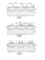
- FIG. 5 shows the stage at which there are provided in a semiconductor substrate 1 of the first conductivity type, in this case n-type silicon having an average doping concentration of about 5.10 14 atoms/cm 3 , zones 33 of the second conductivity type, so in this case p-type, by means of a usual diffusion of impurities via a masking 30 of, for example, silicon oxide with windows 32 extending at a fixed relative centre distance 31. These zones 33 have an average doping concentration of about 3.10 15 atoms/cm 3 .
- zones of the first conductivity type, so in this case n-type, forming the channel regions 7 are provided via a second masking 34, for example also of silicon oxide, with windows 35 extending at the same relative centre distance 31 by means of a usual diffusion of impurities so that the structure shown in Figure 7 is formed.
- the second masking 34 is then arranged so that the channel regions 7 are formed halfway between the zones 33.
- the channel regions 7 are then mutually separated by channel separation zones 8, while they further adjoin the zone 9 extending substantially parallel to the surface 2.
- This zone 9 has a thickness which extends in the direction at right angles to the channel regions and has minima at the centres of the channel regions 7.
- the channel regions 7 have a doping concentration, in this embodiment of about 10' 6 atoms/cm' on an average, which exceeds that of the zone 9, which is in the embodiment about 3.10 15 atoms/ cm on an average and which in turn exceeds that of the substrate 1, which is in the embodiment about 5.10 14 atoms/cm 3 .
- the width of the channel regions 7 is equal to the width of the windows 35 in the second masking 34 plus the distance over which lateral diffusion of the channel regions 7 beneath the masking 34 occurs. This distance is approximately equal to the thickness of the channel regions 7 and amounts, for example, to 1 pm. A limiting factor is the minimum distance which has to be observed between two adjacent windows 35. If a mask can be realized in which this distance is 4 um, the width of the channel regions becomes about 8 um and the width of the channel separation zones 8 becomes about 2 pm when the centre distance is 10 um.
- the slots 17 have in the direction at right angles to the channels 7 a dimension a, which exceeds half the thickness b of the semiconductor zone 9, measured just beside the channel separation zones 8.
- V at a substrate voltage of +15 V and a voltage at the channel separation zones of 0 V, V, can be about O V and V 2 can be about -5 V.
- the slots 17 are obtained in a simple manner when the aforementioned two diffusions are effected so that the zones 9 of the second conductivity type do not contact each other, but are separated by regions 7,1 of the first conductivity type.
Abstract
Description
- The invention relates to an image sensor device comprising a semiconductor substrate of a first conductivity type having a number of surface-adjoining channel regions of the first conductivity type which are directed at right angles to a system of electrodes present on and insulated from the surface, in which during operation charge produced by incident radiation is collected and transported and which are mutually separated by surface-adjoining channel separation zones of the second opposite conductivity type and further adjoin a semiconductor zone of the second conductivity type extending substantially parallel to the surface, the channel regions having a dopant concentration which exceeds that of the semiconductor zone, which in turn exceeds the doping concentration of the semiconductor substrate.
- The invention further relates to a method of manufacturing such a device.
- In such an image sensor device described in GB-A-2069759, during operation such voltages are applied to the electrodes that a pattern of potential wells mutually separated by potential barriers is formed in the channel regions. For a given integration time, charge produced in the semiconductor material by incident radiation is collected in these potential wells. Thus, a charge image corresponding to a radiation image is formed. After the integration time, clock voltages are applied to the electrodes, as a result of which the collected charge packets are transported through the channel regions and are transferred, for example, to a storage register. Such a method is the so-called frame- or field transfer method. Subsequently, the charge is further processed during the next integration period to television input signals.
- Due to the presence of the semiconductor zone extending substantially parallel to the surface, the application of suitable voltages between the electrodes, the semiconductor zone and the substrate will result in a potential variation between the surface and the substrate which exhibits a potential barrier at the area of the semiconductor zone. Thus, charge which, viewed from the surface, is produced above this potential barrier in the semiconductor material will contribute to the formation of the charge image, whereas charge produced beneath this potential barrier will not contribute to the formation of the charge image. Since long-wave radiation can penetrate more deeply into the semiconductor material than short-wave radiation, the spectral sensitivity of the image sensor device is determined by the position of the potential barrier.
- GB-A-2054961 discloses an image sensor device of the kind mentioned in the opening paragraph in which the channel regions have a doping concentration which does not exceed that of the semiconductor zone and the substrate. As a result, charge collected in the channel regions can influence the potential variation between the surface and the semiconductor substrate in such a manner that the potential barrier, which was initially present at the area of the semiconductor zone, disappears when a given quantity of charge is exceeded during the integration period. When during the integration period, due to a local strong irradiation such a quantity of charge is locally produced that the said given quantity is exceeded, the excess of charge can flow away to the semiconductor substrate. Thus, it can be prevented that this excess of charge can spread over a large number of adjacent potential wells present in the channel regions during the integration period. This phenomenon often designated as "blooming" can give rise to very disturbing lines in a television picture, which is formed by means of signals obtained with such an image sensor device.
- The known image sensor device comprises a semiconductor substrate on which two semiconductor layers are disposed of which the upper layer comprises the channel regions having a doping concentration which does not exceed that of the semiconductor substrate. Such a construction cannot be obtained by means of diffusion of impurities in semiconductor materials. In the case of diffusion of impurities in a semiconductor body of the one conductivity type, only a zone of the other conductivity type can be formed whose doping concentration exceeds that of the semiconductor body. In order to be able to manufacture the known image sensor device, a layer of the first conductivity type will have to be grown epitaxially onto a semiconductor substrate. In this layer structure, channel separation zones extending into the semiconductor zone can be formed by means of diffusion of impurities in both layers.
- Another disadvantage of the known image sensor device is that the channel regions have a width which is determined during the manufacture of the channel separation zones. This zones will have a minimum width which is equal to the minimum dimensions of a window required for the diffusion, plus on both sides the distance over which lateral diffusion takes place. This distance is larger in the known image sensor device than the thickness of the layer in which the channel regions are formed. Starting from a desired centre distance between adjacent channel regions, the desired centre distance minus the width of the required diffusion window and well over twice the thickness of the channel regions is then left for the width of the channel regions. In practice, the desired centre distance is, for example, 10 pm, the width of the window is 4 pm and the thickness of the channel regions is 1 Ilm; for the width of the channel regions only about 3 µm is left.
- The known image sensor device consequently has comparatively narrow channel regions and comparatively wide channel separation zones. This is an undesirable situation because thus not only the quantity of charge that can be collected and transported per unit surface area is comparatively small, but also the image sensor device consequently has a comparatively low sensitivity. Charge produced in the channel separation zones can flow away to the semiconductor substrate and will then not contribute to the image formation.
- The invention has inter alia for its object to provide an image sensor device of the kind mentioned in the opening paragraph, in which charge collected in the channel regions also can influence the potential variation between the surface and the semiconductor substrate in such a manner that an excess of charge can flow away to the semiconductor substrate and which has comparatively wide channel regions and comparatively narrow channel separation zones.
- The image sensor device of the kind mentioned in the opening paragraph in accordance with the invention is characterized in that the semiconductor zone has a thickness which varies in the direction at right angles to the channel regions, the thickness housing minima at the centres of the channel regions.
- The image sensor device according to the invention can be manufactured in a simple manner by means of diffusion of impurities in a semiconductor substrate of the first conductivity type. Thus, zones of the second conductivity type can be provided by means of a first masking with windows extending at a fixed relative centre distance and then zones of the first conductivity type forming the channel regions can be provided by means of a second masking with windows extending at the same relative centre distance. The second masking is then arranged so that the channel regions are formed halfway between the zones of the second conductivity type. The channel regions are then mutually separated by surface-adjoining zones of the second conductivity type (the channel separation zones), while they further adjoin a zone of the second conductivity type extending substantially parallel to the surface. This zone has a thickness, which extends in a direction at right angles to the channel regions and has minima at the centres of the channel regions. The channel regions have a doping concentration which exceeds that of the subjacent semiconductor zone, while the latter in turn has a doping concentration which exceeds that of the semiconductor substrate. As a result, an effective anti-blooming is possible.
- In the image sensor device according to the invention, the width of the channel regions is equal to the width of the windows in the second masking plus the distance over which lateral diffusion takes place. This distance is substantially equal to the thickness of the channel regions. In this case a limiting factor is the minimum distance which has to be observed between two windows. With a desired centre distance between the channel regions, the maximum width of these channel regions is equal to this centre distance minus the minimum window distance and plus twice the thickness of the channel regions. In a practical embodiment corresponding to the foregoing, the centre distance is 10 pm, the minimum window width is 4 pm and the thickness of the channel regions is 1 um; the width of the channel regions then becomes at least 8 pm. As compared with the known image sensor device, the image sensor device according to the invention has comparatively wide channel regions and comparatively narrow channel separation zones.
- The invention further relates to a method of manufacturing an image sensor device of the kind mentioned in the opening paragraph. This method is characterized in that zones of the second conductivity type are provided in a semiconductor substrate of the first conductivity type by means of diffusion of impurities through a first masking with windows extending at a fixed relative centre distance and then zones of the first conductivity type forming the channel regions are provided through a second masking with windows extending at the same relative centre distance, the second masking being arranged so that the channel regions are formed halfway between the zones of the second conductivity type.
- Thus, by means of simple diffusion techniques, an image sensor device is obtained, in which the channel regions are mutually separated by surface-adjoining semiconductor zones of the second conductivity type (the channel separation zones) and which further adjoin a semiconductor zone of the second conductivity type. The channel regions have a 'doping concentration which exceeds that of the semiconductor zone, which in turn has a doping concentration which exceeds that of the semiconductor substrate. The semiconductor zone has a thickness which has in the direction at right angles to the channel regions a variation with minima at the centres of the channel regions. The image sensor thus formed can be used in a manner such that the occurrence of blooming is strongly suppressed.
- The invention will be described more fully hereinafter by way of example with reference to the drawing. In the drawing:
- Fig. 1 shows diagrammatically in plan view an embodiment of the image sensor device according to the invention,
- Fig. 2 is a sectional view of the image sensor device of Fig. 1 taken on the line II-II,
- Fig. 3 is a sectional view of the image sensor device of Fig. 1 taken on the line III-III,
- Fig. 4 shows the potential variation in the image sensor device according to the invention in a direction at right angles to the surface, and
- Figures 5, 6 and 7 show successive stages in the manufacture of the image sensor device shown in Figures 1, 2 and 3.
- The Figures are schematic and not drawn to scale, whilst for the sake of clarity in the cross- sections especially the dimensions in the direction of thickness are greatly exaggerated. Semiconductor zones of the same conductivity type are cross-hatched in the same direction; corresponding parts are generally denoted by the same reference numerals.
- Figures 1 to 3 show diagrammatically an image, sensor device comprising a
semiconductor substrate 1 of a first conductivity type, in the example an n-type silicon substrate. Asurface 2 thereof is adjoined by a number ofchannel regions 7 of the first conductivity type which are directed at right angles to a system ofelectrodes channel separation zones 8 of the second opposite conductivity type adjoining thesurface 2 and which further adjoin asemiconductor zone 9 of the second conductivity type extending substantially parallel to thesurface 2. Theelectrodes surface 2 by aninsulating layer 10 of, for example, silicon oxide. - During operation, as will be described hereinafter, such voltages are applied to the
electrodes electrodes 3 is formed in thechannel regions 7. In these potential wells formed beneath theelectrodes semiconductor material first part 11 of the image sensor device a charge image is formed which corresponds to a radiation image. After the integration time, clock pulses are applied to theelectrodes electrodes channel regions 7 and are transferred, for example, to astorage register 16, The charge can then be read from this register during a next integration time for further signal processing. Thestorage register 16 is covered by a reflecting aluminium layer not shown so that the charge in this register cannot be modified by incident radiation. - During operation, voltages are applied between the electrodes, 3, 4, 5 and 6 and the
substrate 1, as a result of which a potential barrier is formed at the area of thesemiconductor zone 9. Charge produced above this potential barrier will contribute to the formation of the charge image, whereas charge produced beneath this potential barrier will not contribute to the formation of this charge image. Since long-wave radiation can penetrate more deeply into the semiconductor material than short-wave radiation, the spectral sensitivity of the image sensor device can be determined by the choice of the position of the potential barrier. - According to the invention, in the image sensor device of the kind described with reference to Figure 1, 2 and 3, the
channel regions 7 have a doping concentration which exceeds that of thesemiconductor zone 9,which in turn exceeds that of thesubstrate 1. In the example, the doping concentration of the n-type channel regions is about 1016 atoms/cm3, the doping concentration of the p-type semiconductor zone 9 is about 3.1015 atoms/cm3 and the doping concentration of the n-type substrate 1 is about 5.1014 atoms/cm3. Thesemiconductor zone 9 further has a thickness which has in the direction at right angles to the channel regions 7 a variation with minima at the centres of thechannel regions 7. Due to these measures, the potential in the image sensor device will have a variation in the direction at right angles to thesurface 2 as shown diagrammatically in Figure 4. In this Figure, the potential V at the centre of thechannel regions 7 is indicated as a function of the distance X from thesurface 2. Thesemiconductor zone 9 is then connected to earth potential and thesemiconductor substrate 1 is connected to a voltage of about +15 V. Thecurve 20 indicates in this Figure the potential variation at the beginning of an integration period. The potential variation has apotential well 21 which is located in thechannel region 7 and apotential barrier 22 which is located at a depth of thesemiconductor 9. During the integration period, the potential variation can vary via thecurve 23 to thecurve 24 due to the negative charge collected in thechannel region 7. When the situation indicated by thecurve 24 is reached, only such a smallpotential barrier 26 is still present between thepotential well 25 in thechannel region 7 and thesubstrate 1 that, when at this area a further quantity of charge is produced, this charge can flow away to thesubstrate 1. Potential wells can be formed in the longitudinal direction of the channel regions by applying to theelectrodes 3, for example, a voltage V2 and by applying to theelectrodes electrodes potential variation electrode 3 thepotential variation 27 is obtained. (In the Figure, the voltage drop across the insulatinglayer 10 is indicated by dotted lines). Thus, it is achieved that an excess of charge in such a potential well will flow away to thesubstrate 1 instead of to adjacent potential wells in thechannel region 7. This phenomenon, which is often designated as "blooming", can give rise to very disturbing lines in a television picture which is formed by means of signals obtained with such an image sensor device. - The "anti-blooming" described can be realized with very practical voltages between the
electrodes semiconductor zone 9 is interrupted at the centres of thechannel regions 7 andexhibits slots 17 at this area. - As will appear from the following, the image sensor device can be manufactured in a simple manner, whereby the width of the
channel regions 7 can be comparatively large and the width of thechannel separation zones 8 can be comparatively small. The image sensor device according to the invention thus has a comparatively high sensitivity. - Figures 5, 6 and 7 show a few successive stages in the manufacture of the image sensor device shown in Figures 1 to 3. Fig. 5 shows the stage at which there are provided in a
semiconductor substrate 1 of the first conductivity type, in this case n-type silicon having an average doping concentration of about 5.1014 atoms/cm3,zones 33 of the second conductivity type, so in this case p-type, by means of a usual diffusion of impurities via a masking 30 of, for example, silicon oxide withwindows 32 extending at a fixedrelative centre distance 31. Thesezones 33 have an average doping concentration of about 3.1015 atoms/cm3. Subsequently, as shown in Figure 6, zones of the first conductivity type, so in this case n-type, forming thechannel regions 7 are provided via asecond masking 34, for example also of silicon oxide, withwindows 35 extending at the samerelative centre distance 31 by means of a usual diffusion of impurities so that the structure shown in Figure 7 is formed. Thesecond masking 34 is then arranged so that thechannel regions 7 are formed halfway between thezones 33. Thechannel regions 7 are then mutually separated bychannel separation zones 8, while they further adjoin thezone 9 extending substantially parallel to thesurface 2. Thiszone 9 has a thickness which extends in the direction at right angles to the channel regions and has minima at the centres of thechannel regions 7. Thechannel regions 7 have a doping concentration, in this embodiment of about 10'6 atoms/cm' on an average, which exceeds that of thezone 9, which is in the embodiment about 3.1015 atoms/ cm on an average and which in turn exceeds that of thesubstrate 1, which is in the embodiment about 5.1014 atoms/cm3. - The width of the
channel regions 7 is equal to the width of thewindows 35 in the second masking 34 plus the distance over which lateral diffusion of thechannel regions 7 beneath the masking 34 occurs. This distance is approximately equal to the thickness of thechannel regions 7 and amounts, for example, to 1 pm. A limiting factor is the minimum distance which has to be observed between twoadjacent windows 35. If a mask can be realized in which this distance is 4 um, the width of the channel regions becomes about 8 um and the width of thechannel separation zones 8 becomes about 2 pm when the centre distance is 10 um. - After an insulating
layer 10 and a system ofelectrodes slots 17 do not extend beneath theelectrodes storage register 16 because they do not fulfil a function here; however, there is no objection against providing them here too. - Preferably, the
slots 17 have in the direction at right angles to the channels 7 a dimension a, which exceeds half the thickness b of thesemiconductor zone 9, measured just beside thechannel separation zones 8. In this case, at a substrate voltage of +15 V and a voltage at the channel separation zones of 0 V, V, can be about O V and V2 can be about -5 V. - In order to utilize charge present in the
channel separation zones 8 as far as possible, thechannel separation zones 8 have in the direction at right angles to the channel regions preferably a dimension c which is smaller than four times the thickness d of thechannel regions 7, measured just beside thechannel separation zones 8. Thus, it is ensured that in the direction at right angles to the channel regions 7 a potential variation is obtained which causes charge produced in thechannel separation zones 8 to flow to theadjacent channel zones 7 and not to thesubstrate 1 via thezone 9. - The
slots 17 are obtained in a simple manner when the aforementioned two diffusions are effected so that thezones 9 of the second conductivity type do not contact each other, but are separated byregions - As a matter of course, the invention is not limited to the embodiment described above, but many variations are possible for those skilled in the art without departing from the scope of the invention. For example, the electrode system present on the
surface 2 may have light windows and may comprise electrodes overlapping each other. Furthermore, the electrode system may form instead of the 4-phase clock system shown a 3- or 2-phase clock system. In the latter case and in the case in which the electrode system has light windows, additional semiconductor zones of the second conductivity type may be formed in the channel regions in order to obtain desired potentials in the channel regions. Furthermore the potential beneath theelectrode 3 can be adjusted as indicated bycurve 28 in Fig. 4, by applying a voltage V3 at theelectrode 3 which is between V, and V2. Thus apotential well 29 is formed as a result of which the sensitivity of the sensor will be improved since charge generated beneathelectrode 3 now will flow to the channel region beneathelectrodes substrate 1 which is the case when the potential is as indicated bycurve 27.
Claims (6)
Priority Applications (1)
| Application Number | Priority Date | Filing Date | Title |
|---|---|---|---|
| AT84201684T ATE32287T1 (en) | 1983-11-24 | 1984-11-20 | RADIATION RESISTANT IMAGE SENSOR ARRANGEMENT AND METHOD OF PRODUCTION. |
Applications Claiming Priority (2)
| Application Number | Priority Date | Filing Date | Title |
|---|---|---|---|
| NL8304035A NL8304035A (en) | 1983-11-24 | 1983-11-24 | BLOOMING INSENSITIVE IMAGE RECORDING DEVICE AND METHOD OF MANUFACTURE THEREOF. |
| NL8304035 | 1983-11-24 |
Publications (2)
| Publication Number | Publication Date |
|---|---|
| EP0143496A1 EP0143496A1 (en) | 1985-06-05 |
| EP0143496B1 true EP0143496B1 (en) | 1988-01-27 |
Family
ID=19842766
Family Applications (1)
| Application Number | Title | Priority Date | Filing Date |
|---|---|---|---|
| EP84201684A Expired EP0143496B1 (en) | 1983-11-24 | 1984-11-20 | Blooming-insensitive image sensor device and method of manufacturing same |
Country Status (13)
| Country | Link |
|---|---|
| US (2) | US4654682A (en) |
| EP (1) | EP0143496B1 (en) |
| JP (1) | JPS60134569A (en) |
| KR (1) | KR920007785B1 (en) |
| AT (1) | ATE32287T1 (en) |
| AU (1) | AU580272B2 (en) |
| CA (1) | CA1218443A (en) |
| DE (1) | DE3469113D1 (en) |
| ES (1) | ES8600594A1 (en) |
| HK (1) | HK82891A (en) |
| IE (1) | IE56332B1 (en) |
| NL (1) | NL8304035A (en) |
| SG (1) | SG51290G (en) |
Families Citing this family (7)
| Publication number | Priority date | Publication date | Assignee | Title |
|---|---|---|---|---|
| DE3586452T2 (en) * | 1984-10-18 | 1993-03-18 | Matsushita Electronics Corp | SOLID IMAGE SENSOR AND METHOD FOR THE PRODUCTION THEREOF. |
| FR2633455B1 (en) * | 1988-06-24 | 1990-08-24 | Thomson Csf | PHOTO-SENSITIVE MATRIX WITH FRAME TRANSFER D.T.C., WITH A VERTICAL ANTI-GLARE SYSTEM, AND METHOD FOR MANUFACTURING SUCH A MATRIX |
| NL9000776A (en) * | 1990-04-03 | 1991-11-01 | Philips Nv | METHOD FOR MANUFACTURING A LOADED-LINKED IMAGE RECORDING DEVICE, AND IMAGE RECORDING DEVICE OBTAINED BY THIS METHOD |
| JPH04335573A (en) * | 1991-05-10 | 1992-11-24 | Sony Corp | Ccd solid-state image sensing element |
| JPH04373274A (en) * | 1991-06-21 | 1992-12-25 | Sony Corp | Ccd solid-state image pickup element |
| DE69329100T2 (en) * | 1992-12-09 | 2001-03-22 | Koninkl Philips Electronics Nv | Charge coupled arrangement |
| JP3276005B2 (en) * | 1998-12-07 | 2002-04-22 | 日本電気株式会社 | Charge coupled device and method of manufacturing the same |
Family Cites Families (13)
| Publication number | Priority date | Publication date | Assignee | Title |
|---|---|---|---|---|
| US4025943A (en) * | 1976-03-22 | 1977-05-24 | Canadian Patents And Development Limited | Photogeneration channel in front illuminated solid state silicon imaging devices |
| US4181542A (en) * | 1976-10-25 | 1980-01-01 | Nippon Gakki Seizo Kabushiki Kaisha | Method of manufacturing junction field effect transistors |
| CH616024A5 (en) * | 1977-05-05 | 1980-02-29 | Centre Electron Horloger | |
| US4173064A (en) * | 1977-08-22 | 1979-11-06 | Texas Instruments Incorporated | Split gate electrode, self-aligned antiblooming structure and method of making same |
| GB2023340B (en) * | 1978-06-01 | 1982-09-02 | Mitsubishi Electric Corp | Integrated circuits |
| US4344222A (en) * | 1979-05-21 | 1982-08-17 | Ibm Corporation | Bipolar compatible electrically alterable read-only memory |
| GB2054961B (en) * | 1979-07-26 | 1983-07-20 | Gen Electric Co Ltd | Excess charge removal oin charge transfer devices |
| US4322882A (en) * | 1980-02-04 | 1982-04-06 | Fairchild Camera & Instrument Corp. | Method for making an integrated injection logic structure including a self-aligned base contact |
| NL8000998A (en) * | 1980-02-19 | 1981-09-16 | Philips Nv | SOLID RECORDING CAMERA WITH A SEMICONDUCTIVE PHOTOSENSITIVE TREAD PLATE. |
| US4450464A (en) * | 1980-07-23 | 1984-05-22 | Matsushita Electric Industrial Co., Ltd. | Solid state area imaging apparatus having a charge transfer arrangement |
| US4373252A (en) * | 1981-02-17 | 1983-02-15 | Fairchild Camera & Instrument | Method for manufacturing a semiconductor structure having reduced lateral spacing between buried regions |
| US4396438A (en) * | 1981-08-31 | 1983-08-02 | Rca Corporation | Method of making CCD imagers |
| US4406052A (en) * | 1981-11-12 | 1983-09-27 | Gte Laboratories Incorporated | Non-epitaxial static induction transistor processing |
-
1983
- 1983-11-24 NL NL8304035A patent/NL8304035A/en not_active Application Discontinuation
-
1984
- 1984-11-13 US US06/671,154 patent/US4654682A/en not_active Expired - Lifetime
- 1984-11-20 AT AT84201684T patent/ATE32287T1/en active
- 1984-11-20 EP EP84201684A patent/EP0143496B1/en not_active Expired
- 1984-11-20 DE DE8484201684T patent/DE3469113D1/en not_active Expired
- 1984-11-21 JP JP59244685A patent/JPS60134569A/en active Granted
- 1984-11-21 ES ES537816A patent/ES8600594A1/en not_active Expired
- 1984-11-21 KR KR1019840007286A patent/KR920007785B1/en not_active IP Right Cessation
- 1984-11-22 CA CA000468453A patent/CA1218443A/en not_active Expired
- 1984-11-22 IE IE2991/84A patent/IE56332B1/en unknown
- 1984-11-23 AU AU35837/84A patent/AU580272B2/en not_active Ceased
-
1986
- 1986-11-14 US US06/930,985 patent/US4697329A/en not_active Expired - Fee Related
-
1990
- 1990-07-04 SG SG512/90A patent/SG51290G/en unknown
-
1991
- 1991-10-24 HK HK828/91A patent/HK82891A/en not_active IP Right Cessation
Also Published As
| Publication number | Publication date |
|---|---|
| CA1218443A (en) | 1987-02-24 |
| IE56332B1 (en) | 1991-06-19 |
| US4697329A (en) | 1987-10-06 |
| ES537816A0 (en) | 1985-09-16 |
| JPS60134569A (en) | 1985-07-17 |
| IE842991L (en) | 1985-05-24 |
| ES8600594A1 (en) | 1985-09-16 |
| KR850004002A (en) | 1985-06-29 |
| KR920007785B1 (en) | 1992-09-17 |
| US4654682A (en) | 1987-03-31 |
| DE3469113D1 (en) | 1988-03-03 |
| ATE32287T1 (en) | 1988-02-15 |
| AU580272B2 (en) | 1989-01-12 |
| EP0143496A1 (en) | 1985-06-05 |
| JPH0527992B2 (en) | 1993-04-22 |
| HK82891A (en) | 1991-11-01 |
| NL8304035A (en) | 1985-06-17 |
| SG51290G (en) | 1990-08-31 |
| AU3583784A (en) | 1985-05-30 |
Similar Documents
| Publication | Publication Date | Title |
|---|---|---|
| US3896485A (en) | Charge-coupled device with overflow protection | |
| US4593303A (en) | Self-aligned antiblooming structure for charge-coupled devices | |
| US4028716A (en) | Bulk channel charge-coupled device with blooming suppression | |
| EP0362344B1 (en) | Solid-state image sensor | |
| US4168444A (en) | Imaging devices | |
| JP2781425B2 (en) | Method for manufacturing solid-state imaging device | |
| US5118631A (en) | Self-aligned antiblooming structure for charge-coupled devices and method of fabrication thereof | |
| EP0239151B1 (en) | Charge-coupled device | |
| EP0143496B1 (en) | Blooming-insensitive image sensor device and method of manufacturing same | |
| EP0915520B1 (en) | Solid-state image pickup device, process for its manufacture, and method of driving the device | |
| EP0453530B1 (en) | Solid-state image sensor | |
| EP0059547B1 (en) | Clock controlled anti-blooming for virtual phase ccd's | |
| KR930011473B1 (en) | Pseudo different shape ccd with short channel effect | |
| EP0125732B1 (en) | Charge transfer device | |
| US5442208A (en) | Charge-coupled device having charge reset | |
| US4992841A (en) | Pseudo uniphase charge coupled device | |
| EP0069649B1 (en) | Self-aligned antiblooming structure for charge-coupled devices and method of fabrication thereof | |
| US4463367A (en) | Frame-transfer charge-coupled image sensor device having channel sounding regions below light-admitting windows | |
| US5005062A (en) | Image sensor device of the frame transfer type | |
| CA1049652A (en) | Charge-coupled area array | |
| GB1576144A (en) | Methods of manufacturing charge transfer devices | |
| JPH0412067B2 (en) | ||
| JP2724889B2 (en) | Charge transfer element | |
| WO1989005039A1 (en) | Blooming control in ccd image sensors | |
| EP0601638B1 (en) | Charge-coupled device |
Legal Events
| Date | Code | Title | Description |
|---|---|---|---|
| PUAI | Public reference made under article 153(3) epc to a published international application that has entered the european phase |
Free format text: ORIGINAL CODE: 0009012 |
|
| AK | Designated contracting states |
Designated state(s): AT BE DE FR GB IT NL SE |
|
| 17P | Request for examination filed |
Effective date: 19851204 |
|
| 17Q | First examination report despatched |
Effective date: 19870317 |
|
| GRAA | (expected) grant |
Free format text: ORIGINAL CODE: 0009210 |
|
| AK | Designated contracting states |
Kind code of ref document: B1 Designated state(s): AT BE DE FR GB IT NL SE |
|
| REF | Corresponds to: |
Ref document number: 32287 Country of ref document: AT Date of ref document: 19880215 Kind code of ref document: T |
|
| REF | Corresponds to: |
Ref document number: 3469113 Country of ref document: DE Date of ref document: 19880303 |
|
| ITF | It: translation for a ep patent filed |
Owner name: ING. C. GREGORJ S.P.A. |
|
| ET | Fr: translation filed | ||
| PLBE | No opposition filed within time limit |
Free format text: ORIGINAL CODE: 0009261 |
|
| STAA | Information on the status of an ep patent application or granted ep patent |
Free format text: STATUS: NO OPPOSITION FILED WITHIN TIME LIMIT |
|
| 26N | No opposition filed | ||
| PGFP | Annual fee paid to national office [announced via postgrant information from national office to epo] |
Ref country code: BE Payment date: 19891114 Year of fee payment: 6 |
|
| PGFP | Annual fee paid to national office [announced via postgrant information from national office to epo] |
Ref country code: AT Payment date: 19891121 Year of fee payment: 6 |
|
| PGFP | Annual fee paid to national office [announced via postgrant information from national office to epo] |
Ref country code: SE Payment date: 19891128 Year of fee payment: 6 |
|
| PGFP | Annual fee paid to national office [announced via postgrant information from national office to epo] |
Ref country code: NL Payment date: 19891130 Year of fee payment: 6 |
|
| PG25 | Lapsed in a contracting state [announced via postgrant information from national office to epo] |
Ref country code: AT Effective date: 19901120 |
|
| PG25 | Lapsed in a contracting state [announced via postgrant information from national office to epo] |
Ref country code: SE Effective date: 19901121 |
|
| PG25 | Lapsed in a contracting state [announced via postgrant information from national office to epo] |
Ref country code: BE Effective date: 19901130 |
|
| BERE | Be: lapsed |
Owner name: N.V. PHILIPS' GLOEILAMPENFABRIEKEN Effective date: 19901130 |
|
| PG25 | Lapsed in a contracting state [announced via postgrant information from national office to epo] |
Ref country code: NL Effective date: 19910601 |
|
| NLV4 | Nl: lapsed or anulled due to non-payment of the annual fee | ||
| ITTA | It: last paid annual fee | ||
| EUG | Se: european patent has lapsed |
Ref document number: 84201684.2 Effective date: 19910705 |
|
| ITPR | It: changes in ownership of a european patent |
Owner name: CAMBIO RAGIONE SOCIALE;PHILIPS ELECTRONICS N.V. |
|
| REG | Reference to a national code |
Ref country code: FR Ref legal event code: CD |
|
| PGFP | Annual fee paid to national office [announced via postgrant information from national office to epo] |
Ref country code: DE Payment date: 19970127 Year of fee payment: 13 |
|
| PG25 | Lapsed in a contracting state [announced via postgrant information from national office to epo] |
Ref country code: DE Free format text: LAPSE BECAUSE OF NON-PAYMENT OF DUE FEES Effective date: 19980801 |
|
| REG | Reference to a national code |
Ref country code: FR Ref legal event code: CD |
|
| PGFP | Annual fee paid to national office [announced via postgrant information from national office to epo] |
Ref country code: GB Payment date: 20011130 Year of fee payment: 18 |
|
| REG | Reference to a national code |
Ref country code: GB Ref legal event code: IF02 |
|
| PG25 | Lapsed in a contracting state [announced via postgrant information from national office to epo] |
Ref country code: GB Free format text: LAPSE BECAUSE OF NON-PAYMENT OF DUE FEES Effective date: 20021120 |
|
| PGFP | Annual fee paid to national office [announced via postgrant information from national office to epo] |
Ref country code: FR Payment date: 20021126 Year of fee payment: 19 |
|
| REG | Reference to a national code |
Ref country code: FR Ref legal event code: TP |
|
| GBPC | Gb: european patent ceased through non-payment of renewal fee | ||
| PG25 | Lapsed in a contracting state [announced via postgrant information from national office to epo] |
Ref country code: FR Free format text: LAPSE BECAUSE OF NON-PAYMENT OF DUE FEES Effective date: 20040730 |
|
| REG | Reference to a national code |
Ref country code: FR Ref legal event code: ST |