EP0142253A2 - Integrierte Schaltung mit Bipolar- und Feldeffekttransistoren - Google Patents
Integrierte Schaltung mit Bipolar- und Feldeffekttransistoren Download PDFInfo
- Publication number
- EP0142253A2 EP0142253A2 EP84306574A EP84306574A EP0142253A2 EP 0142253 A2 EP0142253 A2 EP 0142253A2 EP 84306574 A EP84306574 A EP 84306574A EP 84306574 A EP84306574 A EP 84306574A EP 0142253 A2 EP0142253 A2 EP 0142253A2
- Authority
- EP
- European Patent Office
- Prior art keywords
- base
- type
- lateral
- bipolar
- integrated circuit
- Prior art date
- Legal status (The legal status is an assumption and is not a legal conclusion. Google has not performed a legal analysis and makes no representation as to the accuracy of the status listed.)
- Withdrawn
Links
Images

Classifications
-
- H—ELECTRICITY
- H10—SEMICONDUCTOR DEVICES; ELECTRIC SOLID-STATE DEVICES NOT OTHERWISE PROVIDED FOR
- H10D—INORGANIC ELECTRIC SEMICONDUCTOR DEVICES
- H10D10/00—Bipolar junction transistors [BJT]
- H10D10/60—Lateral BJTs
-
- H—ELECTRICITY
- H10—SEMICONDUCTOR DEVICES; ELECTRIC SOLID-STATE DEVICES NOT OTHERWISE PROVIDED FOR
- H10D—INORGANIC ELECTRIC SEMICONDUCTOR DEVICES
- H10D84/00—Integrated devices formed in or on semiconductor substrates that comprise only semiconducting layers, e.g. on Si wafers or on GaAs-on-Si wafers
- H10D84/40—Integrated devices formed in or on semiconductor substrates that comprise only semiconducting layers, e.g. on Si wafers or on GaAs-on-Si wafers characterised by the integration of at least one component covered by groups H10D12/00 or H10D30/00 with at least one component covered by groups H10D10/00 or H10D18/00, e.g. integration of IGFETs with BJTs
- H10D84/401—Combinations of FETs or IGBTs with BJTs
Definitions
- This invention relates to integrated circuits and in particular to circuits incorporating both bipolar and field effect devices on a common semiconductor chip.
- the invention also relates to a lateral bipolar transistor structure that is compatible with field effect processing techniques.
- the object of the present invention is to minimise or to overcome these disadvantages.
- a bipolar lateral npn transistor formed in a lightly doped p -type well contained in a lightly doped n -type well in a very lightly doped p -type substrate, the transistor including base collector and emitter regions, characterised in that the emitter comprises an n +- type region formed by diffusion through the same window as a further, medium doped, p-type base diffusion, wherein the base diffusion forms a narrow p-type layer between the n emitter and the p well material such that lateral extension of the base side of the collector/base depletion region is restricted thereby providing a narrow lateral base width and ensuring that the transistor, in use, acts predominantly in a lateral mode.
- a lateral bipolar transistor structure overcomes the high cost, low yield, process step of growing epitaxial material on the highly doped buried layers required for low collector resistance in the standard buried collector processes.
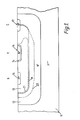
- the npn lateral transistor structure is formed in a very lightly doped p -type silicon substrate 11.
- a lightly doped n -type well 12 is deeply diffused into the substrate 11 and a further lightly doped p -type well 13 is diffused into the well 12.
- a p-type region 14 is diffused to form the intrinsic base, together with a p +- type region 15 to act as a base contact.
- N + regions are added for the emitter 16 and collector contact region 17, during which the emitter is diffused through the same window as the base 14, to end up with a narrow P region surrounding and self aligned to the emitter.
- the collector contact region 17 is disposed across the boundary between the p -type well 13 and the n -type well 12.
- the exact position of the collector is not critical and it is therefore not necessary to provide excessively fine masking tolerance.
- the approximate boundary of the base-collector depletion region is indicated by the dashed lines 21 and 22.
- the inner edge of this depletion region approximately follows the pn junction boundary 18 of the p -type and n -type wells 13 and 12 respectively and terminates at the semiconductor surface between the emitter 16 and collector 17 and immediately adjacent the p-type region surrounding the emitter.
- the boundary is distorted below the region beneath the emitter and collector contact regions such that the non-depleted region of the P-base 13 is wide below the emitter but very narrow at the surface. This defines a narrow active base region in the lateral emitter-collector path thus ensuring that the transistor operates predominantly in its lateral rather than its vertical mode.
- the structure is self aligning thus facilitating processing of the device.
- the transistor structure is formed in an n -type well in a p -type substrate it is compatible with current NMOS or CMOS processing wherein the individual devices are disposed in and isolated by N or P type wells in an opposite polarity substrate.
- Such a construction, compatible with the bipolar transistor of Fig. 1 is shown in Fig. 2.
- the arrangement shown comprises an n-channel (31) and p-channel (32) device each disposed in its respective n -type well 33 and 34.
- devices of only one polarity e.g. NMOS transistors, may be employed. In such a case, and where latch-up is not a problem, the n-channel transistor n -type well 33 is also not required.
- the p +- type and n +- type regions that form the drain and source regions of the two transistors may be formed simultaneously with the corresponding polarity zones of the bipolar transistors that are fabricated on the same chip.
- a further p +- type region 35 may be provided between the two complementary transistors 31 and 32 which zone is connected to the V ss supply of the circuit.
- a similar n +- type region 36 in the n-channel transistor well is coupled to the V DD supply. This reverse biassing of nested well junctions reduces the risk of latch-up of the CMOS portion of the circuitry caused by parasitic bipolar transistor action.
Landscapes
- Metal-Oxide And Bipolar Metal-Oxide Semiconductor Integrated Circuits (AREA)
- Bipolar Transistors (AREA)
Applications Claiming Priority (2)
| Application Number | Priority Date | Filing Date | Title |
|---|---|---|---|
| GB08327868A GB2148589B (en) | 1983-10-18 | 1983-10-18 | Improvements in intergrated circuits |
| GB8327868 | 1983-10-18 |
Publications (2)
| Publication Number | Publication Date |
|---|---|
| EP0142253A2 true EP0142253A2 (de) | 1985-05-22 |
| EP0142253A3 EP0142253A3 (de) | 1986-10-15 |
Family
ID=10550391
Family Applications (1)
| Application Number | Title | Priority Date | Filing Date |
|---|---|---|---|
| EP84306574A Withdrawn EP0142253A3 (de) | 1983-10-18 | 1984-09-27 | Integrierte Schaltung mit Bipolar- und Feldeffekttransistoren |
Country Status (4)
| Country | Link |
|---|---|
| US (1) | US4642667A (de) |
| EP (1) | EP0142253A3 (de) |
| JP (1) | JPS6098670A (de) |
| GB (1) | GB2148589B (de) |
Cited By (1)
| Publication number | Priority date | Publication date | Assignee | Title |
|---|---|---|---|---|
| GR20000100444A (el) * | 2000-12-19 | 2002-10-09 | I.S.D. Λυσεις Ολοκληρωμενων Συστηματων Ανωνυμος Εταιρεια | Διακοπτης πυλης μεταδοσης για προστασια εναντι της ηλεκτροστατικης εκφορτισης (esd) για τεχνολογικες τριπλου πηγαδιου cmos/bicmos |
Families Citing this family (17)
| Publication number | Priority date | Publication date | Assignee | Title |
|---|---|---|---|---|
| US5260226A (en) * | 1987-07-10 | 1993-11-09 | Kabushiki Kaisha Toshiba | Semiconductor device having different impurity concentration wells |
| US5726475A (en) * | 1987-07-10 | 1998-03-10 | Kabushiki Kaisha Toshiba | Semiconductor device having different impurity concentration wells |
| EP0298421B1 (de) * | 1987-07-10 | 1993-12-15 | Kabushiki Kaisha Toshiba | Halbleiterbauelement mit Bereichen unterschiedlicher Störstellenkonzentration |
| US4812891A (en) * | 1987-12-17 | 1989-03-14 | Maxim Integrated Products | Bipolar lateral pass-transistor for CMOS circuits |
| US4862310A (en) * | 1988-04-29 | 1989-08-29 | Dallas Semiconductor Corporation | Low leakage battery protection diode structure |
| USRE35442E (en) * | 1990-07-06 | 1997-02-04 | Sgs-Thomson Microelectronics, S.R.L. | Mixed technology integrated circuit comprising CMOS structures and efficient lateral bipolar transistors with a high early voltage and fabrication thereof |
| US5138413A (en) * | 1990-10-22 | 1992-08-11 | Harris Corporation | Piso electrostatic discharge protection device |
| US5253202A (en) * | 1991-02-05 | 1993-10-12 | International Business Machines Corporation | Word line driver circuit for dynamic random access memories |
| US5994770A (en) * | 1991-07-09 | 1999-11-30 | Dallas Semiconductor Corporation | Portable electronic data carrier |
| US5848541A (en) * | 1994-03-30 | 1998-12-15 | Dallas Semiconductor Corporation | Electrical/mechanical access control systems |
| US5831827A (en) * | 1994-04-28 | 1998-11-03 | Dallas Semiconductor Corporation | Token shaped module for housing an electronic circuit |
| US5604343A (en) * | 1994-05-24 | 1997-02-18 | Dallas Semiconductor Corporation | Secure storage of monetary equivalent data systems and processes |
| US5679944A (en) * | 1994-06-15 | 1997-10-21 | Dallas Semiconductor Corporation | Portable electronic module having EPROM memory, systems and processes |
| US6469362B2 (en) * | 2000-02-15 | 2002-10-22 | Winbond Electronics Corp. | High-gain pnp bipolar junction transistor in a CMOS device and method for forming the same |
| US20050085028A1 (en) * | 2003-10-21 | 2005-04-21 | International Business Machines Corporation | Method and structure to suppress external latch-up |
| US7002218B2 (en) * | 2004-02-26 | 2006-02-21 | Microchip Technology Incorporated | Low capacitance ESD-protection structure under a bond pad |
| CN114929586B (zh) | 2020-01-07 | 2025-10-21 | 因特格拉生物科学有限公司 | 移液管吸头支架系统 |
Family Cites Families (9)
| Publication number | Priority date | Publication date | Assignee | Title |
|---|---|---|---|---|
| US3391035A (en) * | 1965-08-20 | 1968-07-02 | Westinghouse Electric Corp | Method of making p-nu-junction devices by diffusion |
| US3766446A (en) * | 1969-11-20 | 1973-10-16 | Kogyo Gijutsuin | Integrated circuits comprising lateral transistors and process for fabrication thereof |
| US4152717A (en) * | 1975-07-18 | 1979-05-01 | Tokyo Shibaura Electric Co., Ltd. | Complementary MOSFET device |
| US4038107B1 (en) * | 1975-12-03 | 1995-04-18 | Samsung Semiconductor Tele | Method for making transistor structures |
| US4180827A (en) * | 1977-08-31 | 1979-12-25 | International Business Machines Corporation | NPN/PNP Fabrication process with improved alignment |
| CA1131801A (en) * | 1978-01-18 | 1982-09-14 | Johannes A. Appels | Semiconductor device |
| FR2436501A1 (fr) * | 1978-09-15 | 1980-04-11 | Thomson Csf | Transistors bipolaires a tension elevee, circuits integres comportant de tels transistors, et procede de fabrication de tels circuits |
| US4403395A (en) * | 1979-02-15 | 1983-09-13 | Texas Instruments Incorporated | Monolithic integration of logic, control and high voltage interface circuitry |
| JPS56131954A (en) * | 1980-03-19 | 1981-10-15 | Nippon Telegr & Teleph Corp <Ntt> | Semiconductor device |
-
1983
- 1983-10-18 GB GB08327868A patent/GB2148589B/en not_active Expired
-
1984
- 1984-09-27 EP EP84306574A patent/EP0142253A3/de not_active Withdrawn
- 1984-10-04 JP JP59209015A patent/JPS6098670A/ja active Pending
- 1984-10-17 US US06/661,819 patent/US4642667A/en not_active Expired - Fee Related
Cited By (1)
| Publication number | Priority date | Publication date | Assignee | Title |
|---|---|---|---|---|
| GR20000100444A (el) * | 2000-12-19 | 2002-10-09 | I.S.D. Λυσεις Ολοκληρωμενων Συστηματων Ανωνυμος Εταιρεια | Διακοπτης πυλης μεταδοσης για προστασια εναντι της ηλεκτροστατικης εκφορτισης (esd) για τεχνολογικες τριπλου πηγαδιου cmos/bicmos |
Also Published As
| Publication number | Publication date |
|---|---|
| GB2148589A (en) | 1985-05-30 |
| GB2148589B (en) | 1987-04-23 |
| US4642667A (en) | 1987-02-10 |
| EP0142253A3 (de) | 1986-10-15 |
| JPS6098670A (ja) | 1985-06-01 |
| GB8327868D0 (en) | 1983-11-16 |
Similar Documents
| Publication | Publication Date | Title |
|---|---|---|
| US4642667A (en) | Integrated circuits | |
| US4825275A (en) | Integrated bipolar-CMOS circuit isolation for providing different backgate and substrate bias | |
| US5376816A (en) | Bi-cmos integrated circuit device having buried region use in common for bipolar and mos transistors | |
| US5087579A (en) | Method for fabricating an integrated bipolar-CMOS circuit isolation for providing different backgate and substrate bias | |
| US4425516A (en) | Buffer circuit and integrated semiconductor circuit structure formed of bipolar and CMOS transistor elements | |
| US5646433A (en) | Pad protection diode structure | |
| US4912054A (en) | Integrated bipolar-CMOS circuit isolation process for providing different backgate and substrate bias | |
| US4143392A (en) | Composite jfet-bipolar structure | |
| US5060044A (en) | Integrated bipolar-CMOS circuit isolation for providing different backgate and substrate bias | |
| JP2998662B2 (ja) | 半導体装置 | |
| JPH0691200B2 (ja) | 両方向入出力セル | |
| US5172209A (en) | Integral Bi-CMOS logic circuit | |
| JPS58223362A (ja) | 半導体装置 | |
| JPH03276757A (ja) | 半導体装置 | |
| WO2000013234A1 (en) | Integrated circuits | |
| US6229185B1 (en) | CMOS integrated circuit for lessening latch-up susceptibility | |
| JP2553600B2 (ja) | BiMOS半導体集積回路 | |
| JP3108125B2 (ja) | 半導体集積回路 | |
| US4035828A (en) | Semiconductor integrated circuit device | |
| CA1072643A (en) | Logic gate circuits | |
| KR100226798B1 (ko) | 바이씨모스를 이용한 캐스캐이드 구조 | |
| KR930004718B1 (ko) | 인버터 회로 | |
| Murphy et al. | Simplified bipolar technology and its application to systems | |
| KR950007082A (ko) | 정전기 보호장치를 구비하는 반도체 집적회로 및 그 제조방법 | |
| JPH0314232B2 (de) |
Legal Events
| Date | Code | Title | Description |
|---|---|---|---|
| PUAI | Public reference made under article 153(3) epc to a published international application that has entered the european phase |
Free format text: ORIGINAL CODE: 0009012 |
|
| AK | Designated contracting states |
Designated state(s): AT BE CH DE FR IT LI LU NL SE |
|
| RAP1 | Party data changed (applicant data changed or rights of an application transferred) |
Owner name: STC PLC |
|
| PUAL | Search report despatched |
Free format text: ORIGINAL CODE: 0009013 |
|
| AK | Designated contracting states |
Kind code of ref document: A3 Designated state(s): AT BE CH DE FR IT LI LU NL SE |
|
| RAP1 | Party data changed (applicant data changed or rights of an application transferred) |
Owner name: STC PLC |
|
| STAA | Information on the status of an ep patent application or granted ep patent |
Free format text: STATUS: THE APPLICATION IS DEEMED TO BE WITHDRAWN |
|
| 18D | Application deemed to be withdrawn |
Effective date: 19870416 |
|
| RIN1 | Information on inventor provided before grant (corrected) |
Inventor name: MAGEE, TERENCE ERNEST |