EP0140979A1 - Legierung enthaltende flüssigmetall-ion-arten - Google Patents
Legierung enthaltende flüssigmetall-ion-arten Download PDFInfo
- Publication number
- EP0140979A1 EP0140979A1 EP84901430A EP84901430A EP0140979A1 EP 0140979 A1 EP0140979 A1 EP 0140979A1 EP 84901430 A EP84901430 A EP 84901430A EP 84901430 A EP84901430 A EP 84901430A EP 0140979 A1 EP0140979 A1 EP 0140979A1
- Authority
- EP
- European Patent Office
- Prior art keywords
- ion source
- alloy
- liquid metal
- ion
- metal ion
- Prior art date
- Legal status (The legal status is an assumption and is not a legal conclusion. Google has not performed a legal analysis and makes no representation as to the accuracy of the status listed.)
- Granted
Links
- 229910045601 alloy Inorganic materials 0.000 title claims abstract description 54
- 239000000956 alloy Substances 0.000 title claims abstract description 54
- 229910001338 liquidmetal Inorganic materials 0.000 title claims abstract description 21
- 229910052796 boron Inorganic materials 0.000 claims abstract description 29
- 229910052710 silicon Inorganic materials 0.000 claims abstract description 26
- 229910052799 carbon Inorganic materials 0.000 claims abstract description 21
- 229910052698 phosphorus Inorganic materials 0.000 claims abstract description 21
- 239000000203 mixture Substances 0.000 claims abstract description 15
- 229910052785 arsenic Inorganic materials 0.000 claims abstract description 14
- 229910052802 copper Inorganic materials 0.000 claims abstract description 4
- 229910052763 palladium Inorganic materials 0.000 claims abstract description 4
- 229910052737 gold Inorganic materials 0.000 claims abstract description 3
- 229910052697 platinum Inorganic materials 0.000 claims abstract description 3
- 229910052703 rhodium Inorganic materials 0.000 claims abstract description 3
- 229910052707 ruthenium Inorganic materials 0.000 claims abstract description 3
- 229910052709 silver Inorganic materials 0.000 claims abstract description 3
- 150000002500 ions Chemical class 0.000 abstract description 75
- 229910052759 nickel Inorganic materials 0.000 abstract description 2
- PXHVJJICTQNCMI-UHFFFAOYSA-N Nickel Chemical compound [Ni] PXHVJJICTQNCMI-UHFFFAOYSA-N 0.000 abstract 3
- 239000000463 material Substances 0.000 description 36
- 238000002844 melting Methods 0.000 description 23
- 230000008018 melting Effects 0.000 description 22
- 238000010884 ion-beam technique Methods 0.000 description 8
- 229910002056 binary alloy Inorganic materials 0.000 description 7
- OKTJSMMVPCPJKN-UHFFFAOYSA-N Carbon Chemical compound [C] OKTJSMMVPCPJKN-UHFFFAOYSA-N 0.000 description 5
- 229910025794 LaB6 Inorganic materials 0.000 description 5
- 239000011521 glass Substances 0.000 description 5
- 238000010438 heat treatment Methods 0.000 description 5
- 230000002035 prolonged effect Effects 0.000 description 4
- 238000010586 diagram Methods 0.000 description 2
- 238000001035 drying Methods 0.000 description 2
- 230000000694 effects Effects 0.000 description 2
- 230000005684 electric field Effects 0.000 description 2
- 239000006023 eutectic alloy Substances 0.000 description 2
- 229910001385 heavy metal Inorganic materials 0.000 description 2
- 229910052742 iron Inorganic materials 0.000 description 2
- 239000004065 semiconductor Substances 0.000 description 2
- 229910000967 As alloy Inorganic materials 0.000 description 1
- 229910000521 B alloy Inorganic materials 0.000 description 1
- 229910018104 Ni-P Inorganic materials 0.000 description 1
- 229910018536 Ni—P Inorganic materials 0.000 description 1
- 238000004458 analytical method Methods 0.000 description 1
- -1 carbide Inorganic materials 0.000 description 1
- 239000003575 carbonaceous material Substances 0.000 description 1
- 239000002019 doping agent Substances 0.000 description 1
- 238000010894 electron beam technology Methods 0.000 description 1
- 230000006698 induction Effects 0.000 description 1
- 238000002164 ion-beam lithography Methods 0.000 description 1
- 239000007788 liquid Substances 0.000 description 1
- 238000001819 mass spectrum Methods 0.000 description 1
- 229910003465 moissanite Inorganic materials 0.000 description 1
- 239000010453 quartz Substances 0.000 description 1
- 230000005855 radiation Effects 0.000 description 1
- 230000009257 reactivity Effects 0.000 description 1
- 229910010271 silicon carbide Inorganic materials 0.000 description 1
- VYPSYNLAJGMNEJ-UHFFFAOYSA-N silicon dioxide Inorganic materials O=[Si]=O VYPSYNLAJGMNEJ-UHFFFAOYSA-N 0.000 description 1
- 229910021484 silicon-nickel alloy Inorganic materials 0.000 description 1
- 238000005245 sintering Methods 0.000 description 1
- 238000005211 surface analysis Methods 0.000 description 1
- 229910002058 ternary alloy Inorganic materials 0.000 description 1
- 229910052721 tungsten Inorganic materials 0.000 description 1
- 230000008016 vaporization Effects 0.000 description 1
- 238000009834 vaporization Methods 0.000 description 1
Images
Classifications
-
- H—ELECTRICITY
- H01—ELECTRIC ELEMENTS
- H01J—ELECTRIC DISCHARGE TUBES OR DISCHARGE LAMPS
- H01J37/00—Discharge tubes with provision for introducing objects or material to be exposed to the discharge, e.g. for the purpose of examination or processing thereof
- H01J37/02—Details
- H01J37/04—Arrangements of electrodes and associated parts for generating or controlling the discharge, e.g. electron-optical arrangement or ion-optical arrangement
- H01J37/08—Ion sources; Ion guns
-
- H—ELECTRICITY
- H01—ELECTRIC ELEMENTS
- H01J—ELECTRIC DISCHARGE TUBES OR DISCHARGE LAMPS
- H01J27/00—Ion beam tubes
- H01J27/02—Ion sources; Ion guns
- H01J27/022—Details
-
- H—ELECTRICITY
- H01—ELECTRIC ELEMENTS
- H01J—ELECTRIC DISCHARGE TUBES OR DISCHARGE LAMPS
- H01J27/00—Ion beam tubes
- H01J27/02—Ion sources; Ion guns
- H01J27/26—Ion sources; Ion guns using surface ionisation, e.g. field effect ion sources, thermionic ion sources
Definitions
- This invention relates to an ion source material from which ion sources of elements having high melting points, such as B, Si, P or As, can be efficiently and stably drawn out as a single element ion for an extended period of time in a liquid metal ion source.
- ion sources of elements having high melting points such as B, Si, P or As
- liquid metal ion sources having high luminance has been earnestly desired to cope with a remarkable progress of the performance of micro-dry processes (e.g. ion beam lithography, dry process, and micro-doping) and submicron surface analysis.
- micro-dry processes e.g. ion beam lithography, dry process, and micro-doping
- submicron surface analysis e.g. ion beam lithography, dry process, and micro-doping
- the principle of the operation of this liquid metal ion source is as follows.
- an ion source material which has been melted by resistance heating or electron beam heating is supplied to an emitter chip consisting of W, Ta, C and the like, and a strong electric field is then applied to the tip of the chip so as to draw out ions electrolytically dissociated by the electric field from the tip of the chip. It is therefore important for an ion source that an intended ion beam can be drawn out stably for an extended period.
- alloys having melting points of from 40 0 to 1,000°C such as Pt 82 B 18 , Pd 40 Ni 40 B 20 , Pt 27 Ni 13 B 60 , Au 36.5 pt 20 Ge 13.5 B 30 , Pd 40 Ni 40 B 10 As 10 , Pt 72 As 28 , or Pd 24 Sn 68 As 8 , have been used as the ion source material of the kind described above.
- U.S. Patent No. 4,367,429 may be mentioned as an example of the prior art references disclosing such an ion source material.
- the ion source materials involve the critical problem that the life of the ion source is as short as up to 10 hours owing to either of the following reasons.
- the present invention is directed to draw out stably for a long period those ion sources which have high melting points, such as B, Si, P or As.
- the present invention is completed as a result of extensive studies in order to obtain an ion source material (alloy) which has a low melting point and a low vapor pressure at that temperature, which does not at all react, or hardly reacts, with a glass carbon material or a SiC system, a WC system or a LaB 6 system which can be used as the chip material at a high temperature for a long period, and which has high wettability with them.
- Ni provides an eutectic alloy having a relatively low melting point (800 to 1,000°C) with a high melting ion source element such as B, Si, P or As on a lower concentration side (20 to 50 at %) of the element, and then produced ion source materials of the binary alloy systems.
- a high melting ion source element such as B, Si, P or As on a lower concentration side (20 to 50 at %) of the element
- the life of the ion source could be prolonged in comparison with the prior art material, but only by about 100 hours at most.
- the inventors attempted to lower the melting point of the Ni-based binary alloy having a composition close to the eutectic alloy composition, and the vapor pressure and the vis - cosity at that temperature by adding various additional elements, and also to reduce the reactivity with the emitter chip material (principally, glass carbon, carbide, LaB 6 or the like) to improve the wettability.
- the liquid ion source alloy of the present invention consists of at least three elements including Ni, and the sum of at least two elements selected from the group consisting of B, Si, P, C and As is from 32 to 70 at%.
- the alloy it is preferred that at least 1 at% each of the two elements other than Ni are contained in the alloy, because the amount of the additional element(s) to be added to the Ni-based binary alloy is preferably at least 1 at% in order to enhance the effect of the addition. Even if the amount is below 1 at%, the alloy exhibits better characteristics than the binary alloy, because the additional element exerts its effect even in a trace quantity.
- Si, P and/or C for Ni-B alloy B, Si and/or C for Ni-P alloy, B for Ni-Si alloy, and B, Si,P and/or C for Ni-As alloy.
- the liquid metal ion source alloy of the present .invention haying the composition described above has a melting point of below about 1000°C, satisfies the target characteristics described already, and has a long life besides the excellent characteristics.
- the melting point becomes undesirably high.
- a Ni-based alloy which contains B and Si and in which the sum of concentrations of B and Si is from 35 to 70 at% is found suitable and drastically improves the life of the ion source, because not only the melting point is below 1,000°C, but also it hardly reacts with the emitter chip material but has high wettability.
- the melting point and viscosity of the alloy can be further reduced and its wettability with the chip material can be further improved by adding up to 20 at% of P and/or C to the alloy system.
- Ni e.g., P, B, C and/or Si
- T is at least one element selected from the group consisting of B, C and Si
- each of B, C and/or Si is at least 1 at%.
- Ni of the Ni-based alloys was partially substituted (up to 10 at%) by elements such as Cu, Ru, Rh, Pd, Ag, Au or Pt, the melting point of the alloys could be further reduced and the life of the ion source could be further improved.
- the content of the ion source material is preferably limited to 10 at% or below in order to prevent the heavy metal from being incorporated during ion doping.
- the Ni-based ion source material of the present invention obtained in the manner described above can prolong the life of the ion source over 100 hours particularly when a carbide (SiC or WC), LaB 6 or the like is used as the emitter chip material.
- the life can be likewise prolonged in the same way as above by substituting part or the whole of Ni of the Ni-based alloy of the invention by Fe or Co.
- the sum of concentrations of Fe, Co and Ni must be from 70 to 85 at%.
- the ion source material in accordance with the present invention is found to be capable of solving the critical problem of the conventional liquid metal ion sources in that the life is short, and is also found to be an excellent material from which high-melting element ion sources such as B, Si, P or As can be drawn out efficiently and stably for an extended period as a single element ion.
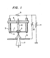
- Figure 1 is a schematic diagram of the ion source using the ion source material of the present invention.
- the ion source was composed of a resistance heater 1 consisting of a sheet-shaped sintered carbon having a width of 2 to 3 mm, a length of 20 mm and a thickness of 200 ⁇ m, an ion source material 2, a current lead-in terminal 3, a set screw 4, an ion drawing-cut electrode 5, a needle-like emitter chip (glass carbon or carbide such as SiC or WC, or LaB6) , a support bed 8, a heating power source 9, a drawing-out power source 10, and a heating power source 11.
- Reference numeral 7 repre- .sents ion beams.
- Ni 43 B 45 Si 10 C 2 , Ni 45 B 45 P 10 and Ni 50 B 30 Si 10 P 5 C 5 alloys were used as the ion source materials for the B ion, Ni 65 P 25 C 10 , Ni 60 P 30 B 10 and Ni 50 Cu 5 P 35 B 10 alloys, as the ion source materials for the P ion, Ni 45 Si 45 B 10 , Ni 35 Si 55 B 10 and Ni 40 Pd 5 Si 45 B 10 alloys, as the ion source materials for the Si ion, and Ni 50 As 40 Si 10 , Ni 50 As 40 B 10 and Ni 45 As 40 B 10 C 5 alloys , as the ion source materials for the As ion. These alloys were produced by plasma melting and RF induction heating.
- the P- or As-containing alloy systems were put into a quartz tube in vacuum after sintering, and were thereafter heated and melted.
- the melting points of these alloys are tabulated in Table 1.
- the melting points of Ni 50 B 50 , Ni 50 Si 50 , Ni 75 P 25 and Ni 6o As 40 alloys are also shown in Table 1 for comparison. It can be understood that the melting points could be further lowered by adding B, P, C, Si, Cu, Pd or the like to the binary alloy systems.
- Ion source samples having a diameter of 1 to 2 mm were produced from the alloys prepared above, were placed on the resistance heater 1 shown in Figure 1 and were melted so as to examine the life of the ion sources. As a result, it was confirmed that when glass carbon or SiC or LaB 6 was used as the emitter chip material, all the samples showed good wettability with the chip, but hardly reacted with the chip, and the ion beams could be drawn out for more than 100 hours.
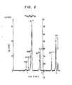
- FIG. 2 shows the mass spectra of ions emitted from an alloy of Ni 45 B 45 Si 10 with an emitted angle of ions in a few m rad as a typical example of the present invention.
- the drawing-out voltage was 10.5 kV
- the total ion current was approximately 150 pA.
- the melting point of the alloy can be lowered and its life as the ion source can be prolonged.
Landscapes
- Chemical & Material Sciences (AREA)
- Engineering & Computer Science (AREA)
- Combustion & Propulsion (AREA)
- Analytical Chemistry (AREA)
- Electron Sources, Ion Sources (AREA)
Applications Claiming Priority (2)
| Application Number | Priority Date | Filing Date | Title |
|---|---|---|---|
| JP65426/83 | 1983-04-15 | ||
| JP58065426A JPS59191225A (ja) | 1983-04-15 | 1983-04-15 | 液体金属イオン種合金 |
Publications (3)
| Publication Number | Publication Date |
|---|---|
| EP0140979A1 true EP0140979A1 (de) | 1985-05-15 |
| EP0140979A4 EP0140979A4 (de) | 1988-01-26 |
| EP0140979B1 EP0140979B1 (de) | 1991-02-27 |
Family
ID=13286735
Family Applications (1)
| Application Number | Title | Priority Date | Filing Date |
|---|---|---|---|
| EP19840901430 Expired EP0140979B1 (de) | 1983-04-15 | 1984-04-13 | Legierung enthaltende flüssigmetall-ion-arten |
Country Status (5)
| Country | Link |
|---|---|
| EP (1) | EP0140979B1 (de) |
| JP (1) | JPS59191225A (de) |
| CA (1) | CA1225229A (de) |
| DE (1) | DE3484167D1 (de) |
| WO (1) | WO1984004202A1 (de) |
Cited By (4)
| Publication number | Priority date | Publication date | Assignee | Title |
|---|---|---|---|---|
| WO1986006210A1 (en) * | 1985-04-08 | 1986-10-23 | Hughes Aircraft Company | Manufacture of liquid metal ion source |
| WO1987006390A3 (en) * | 1986-04-14 | 1987-11-05 | Hughes Aircraft Co | Liquid metal ion source and alloy for ion emission of multiple ionic species |
| WO1987006407A3 (en) * | 1986-04-14 | 1987-11-05 | Hughes Aircraft Co | Liquid metal ion source and alloy |
| EP0248914A4 (de) * | 1985-12-13 | 1988-09-28 | Hitachi Ltd | Quelle flüssiger metallionen. |
Family Cites Families (2)
| Publication number | Priority date | Publication date | Assignee | Title |
|---|---|---|---|---|
| US4367429A (en) * | 1980-11-03 | 1983-01-04 | Hughes Aircraft Company | Alloys for liquid metal ion sources |
| JPS57131360A (en) * | 1981-02-03 | 1982-08-14 | Rikagaku Kenkyusho | Electric field evaporation type ion source using liquid alloy |
-
1983
- 1983-04-15 JP JP58065426A patent/JPS59191225A/ja active Granted
-
1984
- 1984-04-13 DE DE8484901430T patent/DE3484167D1/de not_active Expired - Lifetime
- 1984-04-13 EP EP19840901430 patent/EP0140979B1/de not_active Expired
- 1984-04-13 WO PCT/JP1984/000188 patent/WO1984004202A1/ja not_active Ceased
- 1984-04-16 CA CA000452060A patent/CA1225229A/en not_active Expired
Non-Patent Citations (2)
| Title |
|---|
| JAPANESE JOURNAL OF APPLIED PHYSICS, vol. 21, no. 5, May 1982, pages L277-L278; T. ISHITANI et al.: "Carbon needle emitter for boron and aluminum ion liquid-metal-ion sources" * |
| See also references of WO8404202A1 * |
Cited By (5)
| Publication number | Priority date | Publication date | Assignee | Title |
|---|---|---|---|---|
| WO1986006210A1 (en) * | 1985-04-08 | 1986-10-23 | Hughes Aircraft Company | Manufacture of liquid metal ion source |
| EP0248914A4 (de) * | 1985-12-13 | 1988-09-28 | Hitachi Ltd | Quelle flüssiger metallionen. |
| WO1987006390A3 (en) * | 1986-04-14 | 1987-11-05 | Hughes Aircraft Co | Liquid metal ion source and alloy for ion emission of multiple ionic species |
| WO1987006407A3 (en) * | 1986-04-14 | 1987-11-05 | Hughes Aircraft Co | Liquid metal ion source and alloy |
| US4775818A (en) * | 1986-04-14 | 1988-10-04 | Hughes Aircraft Company | Liquid metal ion source and alloy |
Also Published As
| Publication number | Publication date |
|---|---|
| DE3484167D1 (de) | 1991-04-04 |
| EP0140979B1 (de) | 1991-02-27 |
| JPH0421976B2 (de) | 1992-04-14 |
| EP0140979A4 (de) | 1988-01-26 |
| JPS59191225A (ja) | 1984-10-30 |
| CA1225229A (en) | 1987-08-11 |
| WO1984004202A1 (fr) | 1984-10-25 |
Similar Documents
| Publication | Publication Date | Title |
|---|---|---|
| US4467240A (en) | Ion beam source | |
| EP0248914B1 (de) | Quelle flüssiger metallionen | |
| US4367429A (en) | Alloys for liquid metal ion sources | |
| US6952075B2 (en) | Cold cathode and cold cathode discharge device | |
| US5606141A (en) | Electrical conductor in lamps | |
| US3719854A (en) | Tungsten alloy x-ray target | |
| EP0140979A1 (de) | Legierung enthaltende flüssigmetall-ion-arten | |
| JP3404640B2 (ja) | タングステン電極材 | |
| JP3264775B2 (ja) | 熱電界放射電子銃 | |
| GB1567071A (en) | Filament for alkali metal ionisation detector | |
| US5028756A (en) | Electrode wire for electric spark cutting | |
| US6511632B1 (en) | Cathode material of electron beam device and preparation method thereof | |
| KR100315123B1 (ko) | 전자빔 장치용 음극 물질 | |
| GB2150745A (en) | Liquid metal ion source | |
| Hesse et al. | Development of a cobalt liquid alloy ion source | |
| EP0333369A1 (de) | Matrixkathode aus einer festen Lösung | |
| US5196273A (en) | Tantalum carbide composite materials | |
| JPS6056327A (ja) | 液体金属イオン種合金 | |
| Fane | A sintered nickel matrix cathode | |
| JPS61248335A (ja) | 液体金属イオン源 | |
| JPS6132934A (ja) | 液体金属イオン種合金 | |
| SU1091246A1 (ru) | Способ изготовлени термоэлектронного катода | |
| JPS60249225A (ja) | 液体金属イオン源 | |
| JPS617535A (ja) | 液体金属イオン源 | |
| Bartha | Application of Tungsten Alloys in the Lighting Industry |
Legal Events
| Date | Code | Title | Description |
|---|---|---|---|
| PUAI | Public reference made under article 153(3) epc to a published international application that has entered the european phase |
Free format text: ORIGINAL CODE: 0009012 |
|
| 17P | Request for examination filed |
Effective date: 19841206 |
|
| AK | Designated contracting states |
Designated state(s): DE FR GB NL |
|
| A4 | Supplementary search report drawn up and despatched |
Effective date: 19880126 |
|
| 17Q | First examination report despatched |
Effective date: 19890127 |
|
| GRAA | (expected) grant |
Free format text: ORIGINAL CODE: 0009210 |
|
| RBV | Designated contracting states (corrected) |
Designated state(s): DE GB |
|
| AK | Designated contracting states |
Kind code of ref document: B1 Designated state(s): DE GB |
|
| REF | Corresponds to: |
Ref document number: 3484167 Country of ref document: DE Date of ref document: 19910404 |
|
| K2C3 | Correction of patent specification (complete document) published |
Effective date: 19910227 |
|
| PLBE | No opposition filed within time limit |
Free format text: ORIGINAL CODE: 0009261 |
|
| STAA | Information on the status of an ep patent application or granted ep patent |
Free format text: STATUS: NO OPPOSITION FILED WITHIN TIME LIMIT |
|
| 26N | No opposition filed | ||
| PGFP | Annual fee paid to national office [announced via postgrant information from national office to epo] |
Ref country code: DE Payment date: 19980527 Year of fee payment: 15 |
|
| PGFP | Annual fee paid to national office [announced via postgrant information from national office to epo] |
Ref country code: GB Payment date: 19990325 Year of fee payment: 16 |
|
| PG25 | Lapsed in a contracting state [announced via postgrant information from national office to epo] |
Ref country code: DE Free format text: LAPSE BECAUSE OF NON-PAYMENT OF DUE FEES Effective date: 20000201 |
|
| PG25 | Lapsed in a contracting state [announced via postgrant information from national office to epo] |
Ref country code: GB Free format text: LAPSE BECAUSE OF NON-PAYMENT OF DUE FEES Effective date: 20000413 |
|
| GBPC | Gb: european patent ceased through non-payment of renewal fee |
Effective date: 20000413 |