EP0140246B1 - Dünnschicht-Elektrolumineszenzanzeige - Google Patents
Dünnschicht-Elektrolumineszenzanzeige Download PDFInfo
- Publication number
- EP0140246B1 EP0140246B1 EP19840112241 EP84112241A EP0140246B1 EP 0140246 B1 EP0140246 B1 EP 0140246B1 EP 19840112241 EP19840112241 EP 19840112241 EP 84112241 A EP84112241 A EP 84112241A EP 0140246 B1 EP0140246 B1 EP 0140246B1
- Authority
- EP
- European Patent Office
- Prior art keywords
- layer
- dark field
- display device
- electroluminescent display
- set forth
- Prior art date
- Legal status (The legal status is an assumption and is not a legal conclusion. Google has not performed a legal analysis and makes no representation as to the accuracy of the status listed.)
- Expired
Links
Images
Classifications
-
- H—ELECTRICITY
- H05—ELECTRIC TECHNIQUES NOT OTHERWISE PROVIDED FOR
- H05B—ELECTRIC HEATING; ELECTRIC LIGHT SOURCES NOT OTHERWISE PROVIDED FOR; CIRCUIT ARRANGEMENTS FOR ELECTRIC LIGHT SOURCES, IN GENERAL
- H05B33/00—Electroluminescent light sources
- H05B33/12—Light sources with substantially two-dimensional [2D] radiating surfaces
- H05B33/22—Light sources with substantially two-dimensional [2D] radiating surfaces characterised by the chemical or physical composition or the arrangement of auxiliary dielectric or reflective layers
Definitions
- the present invention relates to an electroluminescent display device with the features of the generic clause of claim 1.
- Electroluminescent devices generally comprise a phosphor layer disposed between two electrode layers with one of the electrodes being transparent so as to permit viewability of the phosphor layer. It is known to provide a dark field layer behind the phosphor layer in order to improve the contrast ratio of the device when using a segmented back electrode layer; that is to say, to provide visibility of the phosphor layer overlying the back electrode segments even under ambient conditions of high brightness. See U.S. Patent 3,560,784 for an example of a dark field layer, the material of which may comprise arsenic sulphide, arsenic selenide, arsenic sulfoselenide or mixtures thereof. However, these arsenic compounds either do not provide a satisfactory dark color or they change color during use.
- CdTe cadmium telluride
- an object of the present invention to provide an improved electroluminescent display device and in particular an improved dark field material for such a device.
- Another object of the present invention is to provide an improved dark field in accordance with the preceding object and which is characterized by an improved contrast ratio of the device.
- Still another object of the present invention is to provide a dark field material in accordance with the preceding objects and which is non-toxic and meets the safety specifications for commercial products required by OSHA (Occupational Safety and Health Act).
- a further object of the present invention is to provide an improved dark field layer in a thin film electroluminescent display device in which for at least some applications, only a single transparent dielectric layer of the device is employed in comparison with the typical first and second transparent dielectric layers used in the past in electroluminescent thin film display devices.
- Still a further object of the present invention is to provide an improved dark field material for a thin film electroluminescent display device in which the dark field layer is formed of constituents which are readily analyzable, and thus precisely controllable, to provide enhanced flexibility in controlling parameters of the dark field layer such as contrast ratio.
- the dark field layer is a composition of a dielectric material with a noble metal.
- the improved dark field layer comprises a composition of a dielectric material, preferably a ceramic, in combination with a noble metal, which in the preferred embodiment is gold.
- the ceramic is preferably magnesium oxide.
- the preferred composition of magnesium oxide and gold may be formed by a sputtering technique, examples of which are described in further detail hereinafter.
- the dark field material for a thin film electroluminescent display device is formed by a composition of a dielectric material with a noble metal.
- the dark field layer serves the basic purpose of enhancing the contrast between the displayed information which is usually in segment form and the background.
- a composition of, for example, magnesium oxide and gold which are co-evaporated, preferably by an electron beam technique, provide a dark field material that is non-toxic, is readily analyzable and meets the safety specifications for commercial products.
- the layer has also been found to unexpectedly provide contrast enhancement.
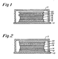
- Fig. 1 there is shown a version of an electroluminescent display device incorporating the dark field of this invention.
- Fig. 2 one of the two transparent dielectric layers shown in Fig. has been removed because, in accordance with the present invention, the improved dark field layer also functions as a substitute for one of the dielectric layers.
- the dielectric/ noble metal composition serves both as the dark field and as the second dielectric.
- a glass substrate 10 on which are formed a number of multiple thin-film layers, which may be enclosed by a glass seal 11. These layers include a transparent electrode 12, a first transparent dielectric layer 14, an electroluminescent phosphor layer 16, a second transparent dielectric layer 18, a dark field layer 20, and a back segmented electrode 22.
- the transparent dielectric layers may be of yttria, and the electroluminescent phosphor layer may be of, for example, zinc sulphide.
- the second transparent dielectric layer 18 is shown, but it is noted that in the embodiment of Fig. 2, this layer is not present.
- the dark field layer 20 in Fig. 2 instead serves both as the dark field and as the second dielectric layer.
- the composition of the dark field layer 20, which in its broadest sense comprises a dielectric material, preferably a ceramic, and a noble metal, preferably gold, may be deposited by co-evaporation using standard deposition techniques.
- co-evaporation is used with e-beam equipment.
- the evaporation may take place in one chamber of a two-chamber system.
- the two chamber system has two e-beam guns, each with its own power supply.
- magnesium oxide may be in pellet form and loaded into one crucible, and gold is disposed in the second crucible.
- the deposition may be measured by means of conventional crystal monitors. One crystal monitor is placed over each crucible being disposed as close as possible to the position where the substrate is.
- the co-evaporation technique using separate crucibles is carried out in a vacuum of preferably better than 133x10-5 Pa (1 x 10- 5 torr).
- the percentage of gold in the composition is instrumental in controlling the resistivity of the cermet.
- control of gold (noble metal) concentration reference is made to EP-A-139281 (priority; 11.10.83. published 2.5.85), assigned to the present assignee.
- the dark field layer had a thickness of 0.5x 10- 6 m (0.5 micron).
- the preferred film thickness is in the range of 500-900 nm. (5000-9000 Angstroms).
- the lateral resistance between back electrode segments is on the order of 10 megohms while the perpendicular resistance across the film thickness is on the order of 1 k ohm or less.
- a contrast ratio of 2:1 is measured at an ambient light level of 2,69 X 10 4 cd/m 2 (2500 foot-candles) with the back electrode segments at 160 volts and 205 cd/m 2 (60 foot-lamberts). With those parameters, display devices have been operated successfully up to 500 hours of operating time.
- sputtering may be used in a reactive atmosphere of say argon and oxygen in a ratio of 70%-30%, respectively.
- composition MgO/Au is that the material itself as well as the process forming it, is non-toxic. Also, the admixed metal (Au) and the metal of the metal oxide (Mg) are two different materials and thus the ratio between these constituents is readily analyzable and, thus, provides for an added degree of control over such parameters of the dark field layer as electrical conductivity and optical absorption.
- the composition may comprise other noble metals in place of the gold such as platinum or silver.
- the dielectric portion of the composition may be a ceramic. This can be a metal oxide or a metal nitride (such as aluminum nitride) or can even be a semiconductor such as silicon dioxide or germanium dioxide.
- the noble metal portion of the composition is in the form of a relatively stable metal thus not tending to react with the metallic in the ceramic portion of the composition.
- the noble metal, such as gold does not readily oxidize if it is mixed with the magnesium oxide.
- the dark field layer may be deposited by techniques other than co-evaporation or electron beam evaporation, such as by sputtering.
Landscapes
- Electroluminescent Light Sources (AREA)
Claims (13)
Applications Claiming Priority (2)
| Application Number | Priority Date | Filing Date | Title |
|---|---|---|---|
| US54022383A | 1983-10-11 | 1983-10-11 | |
| US540223 | 1983-10-11 |
Publications (2)
| Publication Number | Publication Date |
|---|---|
| EP0140246A1 EP0140246A1 (de) | 1985-05-08 |
| EP0140246B1 true EP0140246B1 (de) | 1987-09-16 |
Family
ID=24154526
Family Applications (1)
| Application Number | Title | Priority Date | Filing Date |
|---|---|---|---|
| EP19840112241 Expired EP0140246B1 (de) | 1983-10-11 | 1984-10-11 | Dünnschicht-Elektrolumineszenzanzeige |
Country Status (3)
| Country | Link |
|---|---|
| EP (1) | EP0140246B1 (de) |
| CA (1) | CA1243762A (de) |
| DE (1) | DE3466342D1 (de) |
Cited By (5)
| Publication number | Priority date | Publication date | Assignee | Title |
|---|---|---|---|---|
| WO2006108291A1 (en) * | 2005-04-15 | 2006-10-19 | Ifire Technology Corp. | Magnesium oxide-containing barrier layer for thick dielectric electroluminescent displays |
| US7481887B2 (en) | 2002-05-24 | 2009-01-27 | Micron Technology, Inc. | Apparatus for controlling gas pulsing in processes for depositing materials onto micro-device workpieces |
| US7581511B2 (en) | 2003-10-10 | 2009-09-01 | Micron Technology, Inc. | Apparatus and methods for manufacturing microfeatures on workpieces using plasma vapor processes |
| US7588804B2 (en) | 2002-08-15 | 2009-09-15 | Micron Technology, Inc. | Reactors with isolated gas connectors and methods for depositing materials onto micro-device workpieces |
| US9023436B2 (en) | 2004-05-06 | 2015-05-05 | Micron Technology, Inc. | Methods for depositing material onto microfeature workpieces in reaction chambers and systems for depositing materials onto microfeature workpieces |
Families Citing this family (4)
| Publication number | Priority date | Publication date | Assignee | Title |
|---|---|---|---|---|
| US4849674A (en) * | 1987-03-12 | 1989-07-18 | The Cherry Corporation | Electroluminescent display with interlayer for improved forming |
| GB2195823B (en) * | 1986-09-29 | 1990-01-10 | Ricoh Kk | Thin film electroluminescent device |
| US5445898A (en) * | 1992-12-16 | 1995-08-29 | Westinghouse Norden Systems | Sunlight viewable thin film electroluminescent display |
| US6610352B2 (en) | 2000-12-22 | 2003-08-26 | Ifire Technology, Inc. | Multiple source deposition process |
Family Cites Families (5)
| Publication number | Priority date | Publication date | Assignee | Title |
|---|---|---|---|---|
| US3560784A (en) * | 1968-07-26 | 1971-02-02 | Sigmatron Inc | Dark field, high contrast light emitting display |
| US4312915A (en) * | 1978-01-30 | 1982-01-26 | Massachusetts Institute Of Technology | Cermet film selective black absorber |
| CA1144265A (en) * | 1978-12-29 | 1983-04-05 | John M. Lo | High contrast display device having a dark layer |
| FI60332C (fi) * | 1980-04-24 | 1981-12-10 | Lohja Ab Oy | Elektroluminensstruktur |
| JPS5871589A (ja) * | 1981-10-22 | 1983-04-28 | シャープ株式会社 | 薄膜el素子 |
-
1984
- 1984-10-05 CA CA000464835A patent/CA1243762A/en not_active Expired
- 1984-10-11 EP EP19840112241 patent/EP0140246B1/de not_active Expired
- 1984-10-11 DE DE8484112241T patent/DE3466342D1/de not_active Expired
Cited By (5)
| Publication number | Priority date | Publication date | Assignee | Title |
|---|---|---|---|---|
| US7481887B2 (en) | 2002-05-24 | 2009-01-27 | Micron Technology, Inc. | Apparatus for controlling gas pulsing in processes for depositing materials onto micro-device workpieces |
| US7588804B2 (en) | 2002-08-15 | 2009-09-15 | Micron Technology, Inc. | Reactors with isolated gas connectors and methods for depositing materials onto micro-device workpieces |
| US7581511B2 (en) | 2003-10-10 | 2009-09-01 | Micron Technology, Inc. | Apparatus and methods for manufacturing microfeatures on workpieces using plasma vapor processes |
| US9023436B2 (en) | 2004-05-06 | 2015-05-05 | Micron Technology, Inc. | Methods for depositing material onto microfeature workpieces in reaction chambers and systems for depositing materials onto microfeature workpieces |
| WO2006108291A1 (en) * | 2005-04-15 | 2006-10-19 | Ifire Technology Corp. | Magnesium oxide-containing barrier layer for thick dielectric electroluminescent displays |
Also Published As
| Publication number | Publication date |
|---|---|
| EP0140246A1 (de) | 1985-05-08 |
| CA1243762A (en) | 1988-10-25 |
| DE3466342D1 (en) | 1987-10-22 |
Similar Documents
| Publication | Publication Date | Title |
|---|---|---|
| EP0139281B1 (de) | Dünnschicht-Elektrolumineszenzanzeige | |
| Fraser et al. | Highly conductive, transparent films of sputtered In2− x Sn x O 3− y | |
| EP0781076B1 (de) | Transparentes, leitfähiges Laminat und elektrolumineszentes Element | |
| US4758765A (en) | Black layer for thin film EL display device | |
| US4482841A (en) | Composite dielectrics for low voltage electroluminescent displays | |
| EP0140246B1 (de) | Dünnschicht-Elektrolumineszenzanzeige | |
| JPH05334924A (ja) | 透明導電薄膜の製造法 | |
| US5445898A (en) | Sunlight viewable thin film electroluminescent display | |
| US4455506A (en) | Contrast enhanced electroluminescent device | |
| GB2106317A (en) | Electroluminescent display devices | |
| US4675092A (en) | Method of producing thin film electroluminescent structures | |
| GB2039146A (en) | High contrast display device having a dark layer | |
| Igasaki et al. | Some properties of Al-doped ZnO transparent conducting films prepared by RF reactive sputtering | |
| EP0159531B1 (de) | Dünnfilm-Elektrolumineszenzanordnung | |
| EP0707320A1 (de) | Durchsichtige Leiter mit Zink-Indium-Oxide und Verfahren zur Herstellung dieser Filme | |
| Lloyd | Properties of cadmium stannate films prepared by rf sputtering from powder targets | |
| EP0146967B1 (de) | Fotoleitende Speicherplatte für eine Bildaufnahmeröhre und ihr Herstellungsverfahren | |
| Sichel et al. | Characteristics of the electrochromic materials Au-Wo3 and Pt-Wo3 | |
| US4948529A (en) | Stable high resistance transparent coating | |
| Miyata et al. | Transparent electrode properties of Cd Sn oxide films by dc reactive sputtering | |
| Mauch et al. | Comparison of ZnS: Mn AC TFEL devices prepared by manganese diffusion and coevaporation | |
| EP0109589A1 (de) | Elektrolumineszente Dünnfilm-Anzeigevorrichtung | |
| JP2003346559A (ja) | 透明導電膜、及びその形成方法 | |
| US4040927A (en) | Cadmium tellurite thin films | |
| Mateleshko et al. | Electrooptical properties of DC electroluminescent ZnS: Mn, Cu powder panels with chalcogenide glass intermediate layer |
Legal Events
| Date | Code | Title | Description |
|---|---|---|---|
| PUAI | Public reference made under article 153(3) epc to a published international application that has entered the european phase |
Free format text: ORIGINAL CODE: 0009012 |
|
| 17P | Request for examination filed |
Effective date: 19841011 |
|
| AK | Designated contracting states |
Designated state(s): BE DE FR GB NL |
|
| 17Q | First examination report despatched |
Effective date: 19860613 |
|
| GRAA | (expected) grant |
Free format text: ORIGINAL CODE: 0009210 |
|
| AK | Designated contracting states |
Kind code of ref document: B1 Designated state(s): BE DE FR GB NL |
|
| REF | Corresponds to: |
Ref document number: 3466342 Country of ref document: DE Date of ref document: 19871022 |
|
| PGFP | Annual fee paid to national office [announced via postgrant information from national office to epo] |
Ref country code: NL Payment date: 19871031 Year of fee payment: 4 |
|
| ET | Fr: translation filed | ||
| PLBE | No opposition filed within time limit |
Free format text: ORIGINAL CODE: 0009261 |
|
| STAA | Information on the status of an ep patent application or granted ep patent |
Free format text: STATUS: NO OPPOSITION FILED WITHIN TIME LIMIT |
|
| 26N | No opposition filed | ||
| PG25 | Lapsed in a contracting state [announced via postgrant information from national office to epo] |
Ref country code: GB Effective date: 19891011 |
|
| PG25 | Lapsed in a contracting state [announced via postgrant information from national office to epo] |
Ref country code: BE Effective date: 19891031 |
|
| BERE | Be: lapsed |
Owner name: GTE PRODUCTS CORP. Effective date: 19891031 |
|
| PG25 | Lapsed in a contracting state [announced via postgrant information from national office to epo] |
Ref country code: NL Effective date: 19900501 |
|
| GBPC | Gb: european patent ceased through non-payment of renewal fee | ||
| NLV4 | Nl: lapsed or anulled due to non-payment of the annual fee | ||
| PG25 | Lapsed in a contracting state [announced via postgrant information from national office to epo] |
Ref country code: FR Effective date: 19900629 |
|
| PG25 | Lapsed in a contracting state [announced via postgrant information from national office to epo] |
Ref country code: DE Effective date: 19900703 |
|
| REG | Reference to a national code |
Ref country code: FR Ref legal event code: ST |