EP0138023B1 - Semiconductor vibration detection device with lever structure - Google Patents
Semiconductor vibration detection device with lever structure Download PDFInfo
- Publication number
- EP0138023B1 EP0138023B1 EP84110517A EP84110517A EP0138023B1 EP 0138023 B1 EP0138023 B1 EP 0138023B1 EP 84110517 A EP84110517 A EP 84110517A EP 84110517 A EP84110517 A EP 84110517A EP 0138023 B1 EP0138023 B1 EP 0138023B1
- Authority
- EP
- European Patent Office
- Prior art keywords
- layer
- polysilicon
- etching
- detection device
- forming
- Prior art date
- Legal status (The legal status is an assumption and is not a legal conclusion. Google has not performed a legal analysis and makes no representation as to the accuracy of the status listed.)
- Expired - Lifetime
Links
- 239000004065 semiconductor Substances 0.000 title claims description 43
- 238000001514 detection method Methods 0.000 title claims description 34
- 229910021420 polycrystalline silicon Inorganic materials 0.000 claims description 47
- 229920005591 polysilicon Polymers 0.000 claims description 47
- 125000006850 spacer group Chemical group 0.000 claims description 22
- 238000005530 etching Methods 0.000 claims description 20
- 150000004767 nitrides Chemical class 0.000 claims description 20
- 238000004519 manufacturing process Methods 0.000 claims description 15
- 238000001259 photo etching Methods 0.000 claims description 11
- 229910052796 boron Inorganic materials 0.000 claims description 9
- ZOXJGFHDIHLPTG-UHFFFAOYSA-N Boron Chemical compound [B] ZOXJGFHDIHLPTG-UHFFFAOYSA-N 0.000 claims description 7
- 238000005468 ion implantation Methods 0.000 claims description 5
- ILAHWRKJUDSMFH-UHFFFAOYSA-N boron tribromide Chemical compound BrB(Br)Br ILAHWRKJUDSMFH-UHFFFAOYSA-N 0.000 claims description 4
- 230000000873 masking effect Effects 0.000 claims description 3
- 230000003014 reinforcing effect Effects 0.000 claims description 3
- 229910015845 BBr3 Inorganic materials 0.000 claims description 2
- -1 boron ions Chemical class 0.000 claims description 2
- 238000009792 diffusion process Methods 0.000 claims description 2
- 239000012535 impurity Substances 0.000 claims description 2
- 239000003990 capacitor Substances 0.000 claims 1
- 238000002513 implantation Methods 0.000 claims 1
- 239000010410 layer Substances 0.000 description 43
- 238000000034 method Methods 0.000 description 18
- 239000000243 solution Substances 0.000 description 8
- 238000004518 low pressure chemical vapour deposition Methods 0.000 description 6
- XLYOFNOQVPJJNP-UHFFFAOYSA-N water Substances O XLYOFNOQVPJJNP-UHFFFAOYSA-N 0.000 description 6
- 230000015572 biosynthetic process Effects 0.000 description 4
- BLRPTPMANUNPDV-UHFFFAOYSA-N Silane Chemical compound [SiH4] BLRPTPMANUNPDV-UHFFFAOYSA-N 0.000 description 3
- 230000001133 acceleration Effects 0.000 description 3
- 239000003963 antioxidant agent Substances 0.000 description 3
- 230000003078 antioxidant effect Effects 0.000 description 3
- 230000003647 oxidation Effects 0.000 description 3
- 238000007254 oxidation reaction Methods 0.000 description 3
- NBIIXXVUZAFLBC-UHFFFAOYSA-N Phosphoric acid Chemical compound OP(O)(O)=O NBIIXXVUZAFLBC-UHFFFAOYSA-N 0.000 description 2
- YCIMNLLNPGFGHC-UHFFFAOYSA-N catechol Chemical compound OC1=CC=CC=C1O YCIMNLLNPGFGHC-UHFFFAOYSA-N 0.000 description 2
- 238000005229 chemical vapour deposition Methods 0.000 description 2
- 238000005979 thermal decomposition reaction Methods 0.000 description 2
- PIICEJLVQHRZGT-UHFFFAOYSA-N Ethylenediamine Chemical compound NCCN PIICEJLVQHRZGT-UHFFFAOYSA-N 0.000 description 1
- KRHYYFGTRYWZRS-UHFFFAOYSA-N Fluorane Chemical compound F KRHYYFGTRYWZRS-UHFFFAOYSA-N 0.000 description 1
- XAGFODPZIPBFFR-UHFFFAOYSA-N aluminium Chemical compound [Al] XAGFODPZIPBFFR-UHFFFAOYSA-N 0.000 description 1
- 229910052782 aluminium Inorganic materials 0.000 description 1
- 229910000147 aluminium phosphate Inorganic materials 0.000 description 1
- QVGXLLKOCUKJST-UHFFFAOYSA-N atomic oxygen Chemical compound [O] QVGXLLKOCUKJST-UHFFFAOYSA-N 0.000 description 1
- 239000000470 constituent Substances 0.000 description 1
- 238000010276 construction Methods 0.000 description 1
- 230000005484 gravity Effects 0.000 description 1
- 229960002050 hydrofluoric acid Drugs 0.000 description 1
- 238000002347 injection Methods 0.000 description 1
- 239000007924 injection Substances 0.000 description 1
- 150000002500 ions Chemical class 0.000 description 1
- 239000000463 material Substances 0.000 description 1
- 238000005259 measurement Methods 0.000 description 1
- 239000000203 mixture Substances 0.000 description 1
- 229910052760 oxygen Inorganic materials 0.000 description 1
- 239000001301 oxygen Substances 0.000 description 1
- 238000001020 plasma etching Methods 0.000 description 1
- 230000002787 reinforcement Effects 0.000 description 1
- 238000000926 separation method Methods 0.000 description 1
- 239000002356 single layer Substances 0.000 description 1
- 238000004544 sputter deposition Methods 0.000 description 1
- 239000000126 substance Substances 0.000 description 1
- 238000005406 washing Methods 0.000 description 1
Images

Classifications
-
- H—ELECTRICITY
- H01—ELECTRIC ELEMENTS
- H01L—SEMICONDUCTOR DEVICES NOT COVERED BY CLASS H10
- H01L29/00—Semiconductor devices specially adapted for rectifying, amplifying, oscillating or switching and having potential barriers; Capacitors or resistors having potential barriers, e.g. a PN-junction depletion layer or carrier concentration layer; Details of semiconductor bodies or of electrodes thereof ; Multistep manufacturing processes therefor
- H01L29/66—Types of semiconductor device ; Multistep manufacturing processes therefor
- H01L29/84—Types of semiconductor device ; Multistep manufacturing processes therefor controllable by variation of applied mechanical force, e.g. of pressure
-
- G—PHYSICS
- G01—MEASURING; TESTING
- G01H—MEASUREMENT OF MECHANICAL VIBRATIONS OR ULTRASONIC, SONIC OR INFRASONIC WAVES
- G01H11/00—Measuring mechanical vibrations or ultrasonic, sonic or infrasonic waves by detecting changes in electric or magnetic properties
- G01H11/06—Measuring mechanical vibrations or ultrasonic, sonic or infrasonic waves by detecting changes in electric or magnetic properties by electric means
-
- G—PHYSICS
- G01—MEASURING; TESTING
- G01P—MEASURING LINEAR OR ANGULAR SPEED, ACCELERATION, DECELERATION, OR SHOCK; INDICATING PRESENCE, ABSENCE, OR DIRECTION, OF MOVEMENT
- G01P15/00—Measuring acceleration; Measuring deceleration; Measuring shock, i.e. sudden change of acceleration
- G01P15/02—Measuring acceleration; Measuring deceleration; Measuring shock, i.e. sudden change of acceleration by making use of inertia forces using solid seismic masses
- G01P15/08—Measuring acceleration; Measuring deceleration; Measuring shock, i.e. sudden change of acceleration by making use of inertia forces using solid seismic masses with conversion into electric or magnetic values
- G01P15/0802—Details
-
- G—PHYSICS
- G01—MEASURING; TESTING
- G01P—MEASURING LINEAR OR ANGULAR SPEED, ACCELERATION, DECELERATION, OR SHOCK; INDICATING PRESENCE, ABSENCE, OR DIRECTION, OF MOVEMENT
- G01P15/00—Measuring acceleration; Measuring deceleration; Measuring shock, i.e. sudden change of acceleration
- G01P15/02—Measuring acceleration; Measuring deceleration; Measuring shock, i.e. sudden change of acceleration by making use of inertia forces using solid seismic masses
- G01P15/08—Measuring acceleration; Measuring deceleration; Measuring shock, i.e. sudden change of acceleration by making use of inertia forces using solid seismic masses with conversion into electric or magnetic values
- G01P2015/0805—Measuring acceleration; Measuring deceleration; Measuring shock, i.e. sudden change of acceleration by making use of inertia forces using solid seismic masses with conversion into electric or magnetic values being provided with a particular type of spring-mass-system for defining the displacement of a seismic mass due to an external acceleration
- G01P2015/0822—Measuring acceleration; Measuring deceleration; Measuring shock, i.e. sudden change of acceleration by making use of inertia forces using solid seismic masses with conversion into electric or magnetic values being provided with a particular type of spring-mass-system for defining the displacement of a seismic mass due to an external acceleration for defining out-of-plane movement of the mass
- G01P2015/0825—Measuring acceleration; Measuring deceleration; Measuring shock, i.e. sudden change of acceleration by making use of inertia forces using solid seismic masses with conversion into electric or magnetic values being provided with a particular type of spring-mass-system for defining the displacement of a seismic mass due to an external acceleration for defining out-of-plane movement of the mass for one single degree of freedom of movement of the mass
- G01P2015/0828—Measuring acceleration; Measuring deceleration; Measuring shock, i.e. sudden change of acceleration by making use of inertia forces using solid seismic masses with conversion into electric or magnetic values being provided with a particular type of spring-mass-system for defining the displacement of a seismic mass due to an external acceleration for defining out-of-plane movement of the mass for one single degree of freedom of movement of the mass the mass being of the paddle type being suspended at one of its longitudinal ends
-
- H—ELECTRICITY
- H04—ELECTRIC COMMUNICATION TECHNIQUE
- H04R—LOUDSPEAKERS, MICROPHONES, GRAMOPHONE PICK-UPS OR LIKE ACOUSTIC ELECTROMECHANICAL TRANSDUCERS; DEAF-AID SETS; PUBLIC ADDRESS SYSTEMS
- H04R19/00—Electrostatic transducers
- H04R19/005—Electrostatic transducers using semiconductor materials
Definitions
- the present invention relates to a semiconductor vibration detection device which detects vibration by means of a movable lever installed on a semiconductor base so as to allow a part of the lever to be free to vibrate, in particular, to a process for manufacturing the detection device which makes it possible to produce the movable lever accurately.
- the present inventor has previously invented a vibration detection device as is disclosed in EP-A-0 102 069 falling under Article 54(3) EPC.
- the vibration detection device includes a semiconductor base and a movable lever which is installed on the semiconductor base with at least one of its ends fixed to the semiconductor base so as to allow a part of it to be free to vibrate.
- On the vibrating part of the movable lever there is provided an electrode layer in the form of one united body.
- the movable lever may also consist of a single layer of doped polysilicon which is formed by selectively etching an undoped polysilicon spacer layer.
- On the semiconductor surface, opposite to the movable lever there is prepared a fixed electrode layer.
- a condenser is formed by the electrode layer on the movable lever and the electrode layer on the semiconductor base. This makes it possible to detect vibrations to the device, through measurement of the variations in the condenser capacity due to vibrations of the movable lever.
- the above described type of a vibration detection device is extremely effective. However, there has not yet been found a method of manufacturing such a device with high precision in an easy way and a concrete lever structure facilitating the manufacturing of the device.
- An object of the present invention is to provide a method of manufacturing a semiconductor vibration detection device which allows with high accuracy to obtain a movable lever.
- Another object of the present invention is to provide a semiconductor vibration detection device having a movable lever which can be manufactured in a short time at an inexpensive cost.
- Another object of the present invention is to provide a semiconductor vibration detection device having an enhanced strength of the lever against the forces applied to it in the lateral direction.
- Still another object of the present invention is to provide a semiconductor vibration detection device which is capable of improving the yield rate of manufacture.
- the movable lever has a triple layer structure in which the middle section is a highly doped P + polysilicon layer that is formed to be alkali-etching-proof and the top and the bottom nitride layers sandwiching the middle layer are also alkali-etching-proof.
- FIG. 1 there is shown a semiconductor vibration detection device embodying the present invention.
- the semiconductor vibration detection device essentially comprises a semiconductor base 12 and a movable lever 14 with its own frequency of natural vibration which is installed on the semiconductor base 12 in the form of a cantilever.
- the movable lever 14 has a construction in which an alkali-etching-proof highly doped P + polysilicon layer 16 that serves as an electrode layer is sandwiched by alkali-etching-proof nitride layers 18 and 20.
- an alkali-etching-proof highly doped P + polysilicon layer 16 that serves as an electrode layer is sandwiched by alkali-etching-proof nitride layers 18 and 20.
- the P + region 24, performing the function of a fixed electrode layer forms a condenser together with the highly doped P + polysilicon layer 16 of the movable lever 14.
- the capacity of the condenser varies in accordance with the changes in the separation between the movable lever 14 and the P + region 24. Consequently, by setting up a circuit which can detect the variations in the capacity between the movable lever 14 and the P + region 24, it is possible, by examining the output of the circuit, to determine whether there is applied to the movable lever 14 a vibration corresponding to the frequency of its natural vibration.
- a circuit for detecting the variations in the capacity can be formed compactly on the base 12 in integrated form.
- P + regions 24, 26 and 28 to be used as fixed electrode layer, source and drain are formed in the base 12 of the N type Si.
- a layer of thermally oxidized SiO is formed on the surface of the base 12 to a thickness of, for example, 700 nm (7000 A).
- SiH 4 is thermally decomposed by the low pressure CVD method, for example, at a temperature of about 620°C to form an impurity-free polysilicon layer with thickness of 1 to 3 ⁇ m. Then a polysilicon spacer 30 is formed by photo-etching.
- a nitride layer of thickness of about 50 nm (500 A) is formed all over the surface of the base 12 by thermally decomposing NH 3 and SiH 2 CI 2 at about 750°C by, for example, the low pressure CVD method.
- an antioxidant layer 32 which deters the oxidation of the polysilicon spacer 30 is formed by photo-etching.
- the thermally oxidized Si0 2 layer is removed by photo-etching at the gate region and the contact region 34, and an oxidized gate layer 36 is formed by thermal oxidation in an oxygen atmosphere of, for example, 1,050°C.
- an ion implantation through the oxidized layer for controlling the threshold voltage Vth may be carried out as needed.
- a bottom nitride layer 20 with a thickness of about 30 nm (300 A) is formed all over the surface of the device, for example, by the low pressure CVD method.
- a polysilicon layer of thickness between 500 nm and 1000 nm (5000 A and 10,000 A) is formed all over the device by the low pressure CVD method, for example.
- the polysilicon layer is doped with a high-concentration boron by, for example, the impurity diffusion method using BBr 3 to form a high-concentration P + polysilicon layer 16.
- a cantilever pattern 38 is then formed by plasma etching using CF 4 , and the top nitride layer 18 for the electrode outlet 40 is removed by photo-etching.
- a hole is created by photo-etching at the contact region 34 in the thermally oxidized layer.
- the electrode wirings 42 and 44 are formed by, e.g., sputter deposition and photo-etching.
- a PSG layer with thickness of 1.2 11m, for example, is formed all over the device surface bythermally decomposing SiH 4 and PH 3 at about 400°C by the normal pressure CVD method, for instance.
- a protection layer 46 is formed by photo-etching except for the regions over the bonding pad and the movable lever.
- the entire device surface is etched with an etching solution such as a strong alkaline water solution (a mixture of ethylenediamine, pyrocatechol and water, for instance).
- the polysilicon spacer 30 which contains no boron is etched at a rate of about 50 um/h, completing the semiconductor device as shown in Fig. 1.
- the high-concentration P + polysilicon layer 16 which represents the principal constituent of the movable lever 14 will hardly be etched sideways because of its high concentration of boron. Accordingly, the movable lever 14 can be manufactured with high accuracy.
- the movable lever 14 can be made to have various shapes in the photo-etching process described in conjunction with Fig. 2F.
- the movable lever 14 may be made to have a shape in which its center of gravity is shifted toward the tip side of the lever from its lengthwise midpoint.
- a slender hole may be created at the lengthwise midpoint of the movable lever 14 in order to have, during the final stage of the etching, the strong alkaline water solution to penetrate through the hole to reduce the time required for etching the polysilicon spacer 30 which is directly beneath the movable lever 14.
- the semiconductor vibration detection device formed as described in the foregoing may be applied practically to the detection of engine knocking of automotive vehicles, specific, vibrations of about 7 kHz are generated from the engine during the knocking. Therefore, for detecting knocking, the movable lever 14 needs be formed to have a frequency of natural vibration of 7 kHz.
- the semiconductor vibration detection device has to be arranged in such a way as to have the acceleration and the centrifugal force to be exerted perpendicularly to the arm of the movable lever 14 in order to detect the capacity changes due to the acceleration and the centrifugal force.
- FIG. 3 there is shown another embodiment of the semiconductor vibration detection device in accordance with the present invention.
- the supporting region of the movable lever 14 is reinforced by the arranged formation of a high-concentration P + polysilicon spacer 50.
- Figs. 4A through 41 the processes for Figs. 4A, 4B and 4E through 41 are identical to those of Figs. 2A, 2B and 2D through 2H so that no further explanation will be given.
- those parts that carry the same reference numerals as in Figs. 1 and 2 signify the identical parts in these Figures.
- a bottom nitride layer of about 50 nm (500 A) thickness is formed all over the device surface by the low pressure CVD method, for instance, through thermal decomposition of NH 3 and SiH 2 CL 2 at about 750°C.
- an Si0 2 layer of about 700 nm (7000 A) thickness is formed by thermal decomposition of SiH 4 at about 400°C by, for example, the CVD method at the standard pressure.
- an ion implantation masking 52 is formed by photo-etching through removal of the Si0 2 layer at the reinforcing region of the movable lever.
- a polysilicon spacer 50 is formed in the unmasked portion of the polysilicon spacer 30 by the ion implantation method through injection of boron ions with accelerated energy of 100 keV at the rate of 3 ⁇ 10 16 ions/c m 2 .
- the ion implantation masking 52 is etched away using dilated fluoric acid, and then an antioxidant layer 32 is formed by photo-etching to deter oxidation of the high concentration P + polysilicon spacer 50 and the polysilicon spacer 30.
- the polysilicon spacer 30 is etched away in the final stage with a strong alkaline water solution.
- the rate of etching of the high concentration P + polysilicon spacer 50 by the strong alkaline water solution stays at an extremely low value due to doping of boron at a high concentration. Therefore, the high concentration P + polysilicon spacer 50 survives, completing the formation of the semiconductor device as shown in Fig. 3.
- the semiconductor vibration detection device embodying the present invention includes a movable lever and an oppositely situated fixed electrode.
- the movable lever is fastened to the semiconductor base with at least one of its ends and includes a vibrating part which, incorporating an electrode as a unified body, extends approximately parallel to the semiconductor base.
- the fixed electrode is formed on the semiconductor base opposite to the vibrating part of the movable lever. Between the electrode on the movable lever and the fixed electrode there is formed a condenser.
- the movable lever has a triple layer structure in which a highly doped P + polysilicon layer that is formed to be alkali-etching-proof is covered by alkali-etching-proof nitride layers on both sides.
- the device has the following features.
Landscapes
- Physics & Mathematics (AREA)
- General Physics & Mathematics (AREA)
- Engineering & Computer Science (AREA)
- Microelectronics & Electronic Packaging (AREA)
- Power Engineering (AREA)
- Ceramic Engineering (AREA)
- Condensed Matter Physics & Semiconductors (AREA)
- Computer Hardware Design (AREA)
- Pressure Sensors (AREA)
- Weting (AREA)
- Measurement Of Mechanical Vibrations Or Ultrasonic Waves (AREA)
- Semiconductor Integrated Circuits (AREA)
Description
- The present invention relates to a semiconductor vibration detection device which detects vibration by means of a movable lever installed on a semiconductor base so as to allow a part of the lever to be free to vibrate, in particular, to a process for manufacturing the detection device which makes it possible to produce the movable lever accurately.
- In recent years, demand for detecting machinery vibrations with high precision has been increasing. In particular, need has been in existence for a vibration detection device which is capable of measuring minute vibration in a reliable manner.
- The present inventor has previously invented a vibration detection device as is disclosed in EP-A-0 102 069 falling under Article 54(3) EPC. The vibration detection device includes a semiconductor base and a movable lever which is installed on the semiconductor base with at least one of its ends fixed to the semiconductor base so as to allow a part of it to be free to vibrate. On the vibrating part of the movable lever, there is provided an electrode layer in the form of one united body. The movable lever may also consist of a single layer of doped polysilicon which is formed by selectively etching an undoped polysilicon spacer layer. On the semiconductor surface, opposite to the movable lever, there is prepared a fixed electrode layer. In this way, a condenser is formed by the electrode layer on the movable lever and the electrode layer on the semiconductor base. This makes it possible to detect vibrations to the device, through measurement of the variations in the condenser capacity due to vibrations of the movable lever. The above described type of a vibration detection device is extremely effective. However, there has not yet been found a method of manufacturing such a device with high precision in an easy way and a concrete lever structure facilitating the manufacturing of the device.
- An object of the present invention is to provide a method of manufacturing a semiconductor vibration detection device which allows with high accuracy to obtain a movable lever.
- Another object of the present invention is to provide a semiconductor vibration detection device having a movable lever which can be manufactured in a short time at an inexpensive cost.
- Another object of the present invention is to provide a semiconductor vibration detection device having an enhanced strength of the lever against the forces applied to it in the lateral direction.
- Still another object of the present invention is to provide a semiconductor vibration detection device which is capable of improving the yield rate of manufacture.
- Briefly described, these and other objects of the present invention are accomplished by the provision of an improved semiconductor vibration detection device and corresponding methods of fabrication as set out in the claims. According to the invention, the movable lever has a triple layer structure in which the middle section is a highly doped P+ polysilicon layer that is formed to be alkali-etching-proof and the top and the bottom nitride layers sandwiching the middle layer are also alkali-etching-proof.
- These and other objects, features and advantages of the present invention will be more apparent from the following description of a preferred embodiment, taken in conjunction with the accompanying drawings, in which:
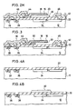
- Fig. 1 is a cross section view of a semiconductor vibration detection device embodying the present invention;
- Figs. 2A through 2H show processes for manufacturing the semiconductor vibration detection device shown in Fig. 1;
- Fig. 3 is a cross section view of another embodiment of the semiconductor vibration detection device in accordance with the present invention; and
- Figs. 4A through 4H show the processes for manufacturing the semiconductor vibration detection device shown in Fig. 3.
- Referring to Fig. 1, there is shown a semiconductor vibration detection device embodying the present invention.
- The semiconductor vibration detection device essentially comprises a
semiconductor base 12 and amovable lever 14 with its own frequency of natural vibration which is installed on thesemiconductor base 12 in the form of a cantilever. Themovable lever 14 has a construction in which an alkali-etching-proof highly doped P+ polysilicon layer 16 that serves as an electrode layer is sandwiched by alkali-etching-proof nitride layers movable lever 14, there is formed on the semiconductor base 12 a P+ region 24 via a thermally oxidized Si02 layer 22. The P+ region 24, performing the function of a fixed electrode layer, forms a condenser together with the highly doped P+ polysilicon layer 16 of themovable lever 14. Therefore, if the.movable lever 14 resonates to an external vibration, the capacity of the condenser varies in accordance with the changes in the separation between themovable lever 14 and the P+ region 24. Consequently, by setting up a circuit which can detect the variations in the capacity between themovable lever 14 and the P+ region 24, it is possible, by examining the output of the circuit, to determine whether there is applied to the movable lever 14 a vibration corresponding to the frequency of its natural vibration. Such a circuit for detecting the variations in the capacity can be formed compactly on thebase 12 in integrated form. - Now, the manufacturing processes for the semiconductor vibration detection device will be described by referring to Figs. 2A through 2H.
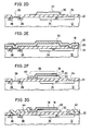
- As shown in Fig. 2A, P+ regions 24, 26 and 28 to be used as fixed electrode layer, source and drain, are formed in the
base 12 of the N type Si. On the surface of thebase 12 there is formed a layer of thermally oxidized SiO to a thickness of, for example, 700 nm (7000 A). - In Fig. 2B, all over the surface of the
base 12, SiH4 is thermally decomposed by the low pressure CVD method, for example, at a temperature of about 620°C to form an impurity-free polysilicon layer with thickness of 1 to 3 µm. Then apolysilicon spacer 30 is formed by photo-etching. - In Fig. 2C, next, a nitride layer of thickness of about 50 nm (500 A) is formed all over the surface of the
base 12 by thermally decomposing NH3 and SiH2CI2 at about 750°C by, for example, the low pressure CVD method. Then, anantioxidant layer 32 which deters the oxidation of thepolysilicon spacer 30 is formed by photo-etching. - In Fig. 2D, the thermally oxidized Si02 layer is removed by photo-etching at the gate region and the
contact region 34, and an oxidizedgate layer 36 is formed by thermal oxidation in an oxygen atmosphere of, for example, 1,050°C. Following this, an ion implantation through the oxidized layer for controlling the threshold voltage Vth may be carried out as needed. - In Fig. 2E, after removal of the
antioxidant layer 32 by hot phosphoric acid (150°C), abottom nitride layer 20 with a thickness of about 30 nm (300 A) is formed all over the surface of the device, for example, by the low pressure CVD method. Then, a polysilicon layer of thickness between 500 nm and 1000 nm (5000 A and 10,000 A) is formed all over the device by the low pressure CVD method, for example. The polysilicon layer is doped with a high-concentration boron by, for example, the impurity diffusion method using BBr3 to form a high-concentration P+ polysilicon layer 16. Following this, atop nitride layer 18, which is about 2 nm (20 A) thicker than thebottom nitride layer 20, is formed all over the device surface by, for example, the low pressure CVD method. - In Fig. 2F, a
cantilever pattern 38 is then formed by plasma etching using CF4, and thetop nitride layer 18 for theelectrode outlet 40 is removed by photo-etching. - In Fig. 2G, a hole is created by photo-etching at the
contact region 34 in the thermally oxidized layer. Then, theelectrode wirings - In Fig. 2H, a PSG layer with thickness of 1.2 11m, for example, is formed all over the device surface bythermally decomposing SiH4 and PH3 at about 400°C by the normal pressure CVD method, for instance. Then, a
protection layer 46 is formed by photo-etching except for the regions over the bonding pad and the movable lever. As the last step, the entire device surface is etched with an etching solution such as a strong alkaline water solution (a mixture of ethylenediamine, pyrocatechol and water, for instance). With this process, thepolysilicon spacer 30 which contains no boron is etched at a rate of about 50 um/h, completing the semiconductor device as shown in Fig. 1. During this process, the high-concentration P+ polysilicon layer 16 which represents the principal constituent of themovable lever 14 will hardly be etched sideways because of its high concentration of boron. Accordingly, themovable lever 14 can be manufactured with high accuracy. - It might be mentioned that the
movable lever 14 can be made to have various shapes in the photo-etching process described in conjunction with Fig. 2F. For instance, themovable lever 14 may be made to have a shape in which its center of gravity is shifted toward the tip side of the lever from its lengthwise midpoint. Moreover, a slender hole may be created at the lengthwise midpoint of themovable lever 14 in order to have, during the final stage of the etching, the strong alkaline water solution to penetrate through the hole to reduce the time required for etching thepolysilicon spacer 30 which is directly beneath themovable lever 14. - The semiconductor vibration detection device formed as described in the foregoing may be applied practically to the detection of engine knocking of automotive vehicles, specific, vibrations of about 7 kHz are generated from the engine during the knocking. Therefore, for detecting knocking, the
movable lever 14 needs be formed to have a frequency of natural vibration of 7 kHz. On the other hand, for applications to the acceleration sensor and the tachometer, the semiconductor vibration detection device has to be arranged in such a way as to have the acceleration and the centrifugal force to be exerted perpendicularly to the arm of themovable lever 14 in order to detect the capacity changes due to the acceleration and the centrifugal force. - Referring to Fig. 3, there is shown another embodiment of the semiconductor vibration detection device in accordance with the present invention. In this embodiment, the supporting region of the
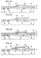
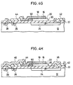
movable lever 14 is reinforced by the arranged formation of a high-concentration P+ polysilicon spacer 50. - Now, the manufacturing processes of the second embodiment of the semiconductor vibration detection device in accordance with the present invention will be described by referring to Figs. 4A through 41. Here, the processes for Figs. 4A, 4B and 4E through 41 are identical to those of Figs. 2A, 2B and 2D through 2H so that no further explanation will be given. Moreover, those parts that carry the same reference numerals as in Figs. 1 and 2 signify the identical parts in these Figures.
- As shown in Fig. 4C, a bottom nitride layer of about 50 nm (500 A) thickness is formed all over the device surface by the low pressure CVD method, for instance, through thermal decomposition of NH3 and SiH2CL2 at about 750°C. On top of it, there is formed an Si02 layer of about 700 nm (7000 A) thickness through thermal decomposition of SiH4 at about 400°C by, for example, the CVD method at the standard pressure. Then, an ion implantation masking 52 is formed by photo-etching through removal of the Si02 layer at the reinforcing region of the movable lever. Following this, a
polysilicon spacer 50 is formed in the unmasked portion of thepolysilicon spacer 30 by the ion implantation method through injection of boron ions with accelerated energy of 100 keV at the rate of 3×10¹⁶ ions/cm 2. - In Fig. 4D, the ion implantation masking 52 is etched away using dilated fluoric acid, and then an
antioxidant layer 32 is formed by photo-etching to deter oxidation of the high concentration P+ polysilicon spacer 50 and thepolysilicon spacer 30. Subsequent to this, via processes of Figs. 4E through 41, thepolysilicon spacer 30 is etched away in the final stage with a strong alkaline water solution. During the final process, the rate of etching of the high concentration P+ polysilicon spacer 50 by the strong alkaline water solution stays at an extremely low value due to doping of boron at a high concentration. Therefore, the high concentration P+ polysilicon spacer 50 survives, completing the formation of the semiconductor device as shown in Fig. 3. - Through reinforcement of the supporting region of the movable lever, it becomes possible to prevent the warping of the movable lever. Due to the increased strength against the lateral forces of the movable lever thus obtained, it becomes possible to suppress the objection that the movable lever tends to break, for example, during etching or washing with water. This leads to an improvement regarding the yield for the formation of the movable lever.
- In summary, the semiconductor vibration detection device embodying the present invention includes a movable lever and an oppositely situated fixed electrode. The movable lever is fastened to the semiconductor base with at least one of its ends and includes a vibrating part which, incorporating an electrode as a unified body, extends approximately parallel to the semiconductor base. The fixed electrode is formed on the semiconductor base opposite to the vibrating part of the movable lever. Between the electrode on the movable lever and the fixed electrode there is formed a condenser. The movable lever has a triple layer structure in which a highly doped P+ polysilicon layer that is formed to be alkali-etching-proof is covered by alkali-etching-proof nitride layers on both sides. The device has the following features.
- (1) In order to form the movable lever in the final stage, it is only necessary to etch away the polysilicon surrounding the movable lever with an alkaline etching solution. Then, the etching of polysilicon with an alkaline etching solution does not utilize anisotropy so that etching can proceed from all directions. Therefore, the formation of the movable lever can be accomplished in a short time (for instance, about 2 hours for a movable lever with a width of 100 µm) without regard to the length of the movable lever.
- (2) By to the reduction in the etching time in the final stage, it now becomes possible to use inexpensive aluminum and PSG film as materials for electrodes and protecting layers, respectively, in spite of the fact that both substances possess certain etching rate against the alkaline etching solution. This will contribute to reduce the cost for manufacturing the semiconductor vibration detection device.
- (3) Since anisotropy is not utilized in conjunction with the etching, there exists no requirement for installing an ultra-high precision orientation flat on the wafer and for carrying out the direction setting for each side of the pattern for the etching window. This circumstance facilitates the etching process, and makes it possible to manufacture the movable lever in a highly precise manner.
Claims (9)
Applications Claiming Priority (2)
| Application Number | Priority Date | Filing Date | Title |
|---|---|---|---|
| JP58163270A JPS6055655A (en) | 1983-09-07 | 1983-09-07 | Semiconductor device having beam structure |
| JP163270/83 | 1983-09-07 |
Publications (3)
| Publication Number | Publication Date |
|---|---|
| EP0138023A2 EP0138023A2 (en) | 1985-04-24 |
| EP0138023A3 EP0138023A3 (en) | 1986-11-20 |
| EP0138023B1 true EP0138023B1 (en) | 1990-12-19 |
Family
ID=15770613
Family Applications (1)
| Application Number | Title | Priority Date | Filing Date |
|---|---|---|---|
| EP84110517A Expired - Lifetime EP0138023B1 (en) | 1983-09-07 | 1984-09-04 | Semiconductor vibration detection device with lever structure |
Country Status (4)
| Country | Link |
|---|---|
| US (1) | US4571661A (en) |
| EP (1) | EP0138023B1 (en) |
| JP (1) | JPS6055655A (en) |
| DE (1) | DE3483764D1 (en) |
Families Citing this family (43)
| Publication number | Priority date | Publication date | Assignee | Title |
|---|---|---|---|---|
| JPS6197572A (en) * | 1984-10-19 | 1986-05-16 | Nissan Motor Co Ltd | Manufacture of semiconductor acceleration sensor |
| US4812888A (en) * | 1984-11-11 | 1989-03-14 | Cornell Research Foundation, Inc. | Suspended gate field effect semiconductor pressure transducer device |
| US4674319A (en) * | 1985-03-20 | 1987-06-23 | The Regents Of The University Of California | Integrated circuit sensor |
| JPS61234064A (en) * | 1985-04-10 | 1986-10-18 | Nissan Motor Co Ltd | Semiconductor vibration detector |
| DE3515349A1 (en) * | 1985-04-27 | 1986-10-30 | Messerschmitt-Bölkow-Blohm GmbH, 8012 Ottobrunn | ELECTRICAL TRANSMITTER FOR MEASURING MECHANICAL SIZES |
| FR2599833B1 (en) * | 1986-06-10 | 1992-02-14 | Metravib Sa | INTEGRATED MECHANICAL SENSOR ON SILICON AND MANUFACTURING METHOD |
| US4948757A (en) * | 1987-04-13 | 1990-08-14 | General Motors Corporation | Method for fabricating three-dimensional microstructures and a high-sensitivity integrated vibration sensor using such microstructures |
| US5343064A (en) * | 1988-03-18 | 1994-08-30 | Spangler Leland J | Fully integrated single-crystal silicon-on-insulator process, sensors and circuits |
| US4996627A (en) * | 1989-01-30 | 1991-02-26 | Dresser Industries, Inc. | High sensitivity miniature pressure transducer |
| US6864677B1 (en) | 1993-12-15 | 2005-03-08 | Kazuhiro Okada | Method of testing a sensor |
| DE4000903C1 (en) * | 1990-01-15 | 1990-08-09 | Robert Bosch Gmbh, 7000 Stuttgart, De | |
| US5421213A (en) * | 1990-10-12 | 1995-06-06 | Okada; Kazuhiro | Multi-dimensional force detector |
| US6314823B1 (en) * | 1991-09-20 | 2001-11-13 | Kazuhiro Okada | Force detector and acceleration detector and method of manufacturing the same |
| FR2700065B1 (en) * | 1992-12-28 | 1995-02-10 | Commissariat Energie Atomique | Method of manufacturing accelerometers using silicon on insulator technology. |
| US5635629A (en) * | 1993-08-03 | 1997-06-03 | Nippondenso Co., Ltd. | Knock sensor |
| JP3213945B2 (en) * | 1993-08-03 | 2001-10-02 | 株式会社デンソー | Knock sensor |
| JP3385688B2 (en) * | 1993-12-13 | 2003-03-10 | 株式会社デンソー | Semiconductor yaw rate sensor and method of manufacturing the same |
| DE4445553A1 (en) * | 1993-12-21 | 1995-06-22 | Nippon Denso Co | Semiconductor accelerometer for motor vehicle engine or safety control |
| US5508231A (en) * | 1994-03-07 | 1996-04-16 | National Semiconductor Corporation | Apparatus and method for achieving mechanical and thermal isolation of portions of integrated monolithic circuits |
| JP3435844B2 (en) * | 1994-03-07 | 2003-08-11 | 株式会社デンソー | Semiconductor acceleration sensor and manufacturing method thereof |
| JP3269274B2 (en) * | 1994-03-15 | 2002-03-25 | 株式会社デンソー | Acceleration sensor |
| US5578843A (en) * | 1994-10-06 | 1996-11-26 | Kavlico Corporation | Semiconductor sensor with a fusion bonded flexible structure |
| JP3435850B2 (en) * | 1994-10-28 | 2003-08-11 | 株式会社デンソー | Semiconductor dynamic quantity sensor and method of manufacturing the same |
| US5550090A (en) * | 1995-09-05 | 1996-08-27 | Motorola Inc. | Method for fabricating a monolithic semiconductor device with integrated surface micromachined structures |
| US5942791A (en) * | 1996-03-06 | 1999-08-24 | Gec-Marconi Limited | Micromachined devices having microbridge structure |
| GB9604786D0 (en) * | 1996-03-06 | 1996-09-25 | Marconi Gec Ltd | Micromachined devices |
| JPH102912A (en) * | 1996-06-14 | 1998-01-06 | Mitsubishi Electric Corp | Semiconductor-acceleration sensor and its manufacture |
| US5966617A (en) * | 1996-09-20 | 1999-10-12 | Kavlico Corporation | Multiple local oxidation for surface micromachining |
| WO1998024119A1 (en) * | 1996-11-22 | 1998-06-04 | Siemens Aktiengesellschaft | Process for manufacturing micromechanical functional elements |
| US5870482A (en) * | 1997-02-25 | 1999-02-09 | Knowles Electronics, Inc. | Miniature silicon condenser microphone |
| US6552469B1 (en) * | 1998-06-05 | 2003-04-22 | Knowles Electronics, Llc | Solid state transducer for converting between an electrical signal and sound |
| US6091125A (en) * | 1998-12-02 | 2000-07-18 | Northeastern University | Micromechanical electronic device |
| US6651504B1 (en) | 1999-09-16 | 2003-11-25 | Ut-Battelle, Llc | Acoustic sensors using microstructures tunable with energy other than acoustic energy |
| DE10006035A1 (en) * | 2000-02-10 | 2001-08-16 | Bosch Gmbh Robert | Micro-mechanical component production, used as sensor element or actuator element, comprises providing functional element and/or functional layer with protective layer |
| DE60118208T2 (en) * | 2000-08-11 | 2007-04-12 | Knowles Electronics, LLC, Itasca | WIDE BAND MINIATURE CONVERTER |
| US6710417B2 (en) * | 2001-09-27 | 2004-03-23 | Seagate Technology Llc | Armor coated MEMS devices |
| KR100419233B1 (en) * | 2002-03-11 | 2004-02-21 | 삼성전자주식회사 | MEMS device and a fabrication method thereof |
| US6767751B2 (en) * | 2002-05-28 | 2004-07-27 | Silicon Light Machines, Inc. | Integrated driver process flow |
| EP1445670A1 (en) | 2003-02-06 | 2004-08-11 | ETA SA Manufacture Horlogère Suisse | Balance-spring resonator spiral and its method of fabrication |
| JP2007111831A (en) * | 2005-10-21 | 2007-05-10 | Seiko Epson Corp | Method for manufacturing mems element, and mems element |
| EP1818736A1 (en) * | 2006-02-09 | 2007-08-15 | The Swatch Group Research and Development Ltd. | Shockproof collet |
| EP2105807B1 (en) * | 2008-03-28 | 2015-12-02 | Montres Breguet SA | Monobloc elevated curve spiral and method for manufacturing same |
| JP6604626B2 (en) | 2015-08-21 | 2019-11-13 | 国立大学法人東北大学 | Detection device |
Family Cites Families (6)
| Publication number | Priority date | Publication date | Assignee | Title |
|---|---|---|---|---|
| US3738880A (en) * | 1971-06-23 | 1973-06-12 | Rca Corp | Method of making a semiconductor device |
| FR2143553B1 (en) * | 1971-06-29 | 1974-05-31 | Sescosem | |
| GB1417170A (en) * | 1972-12-22 | 1975-12-10 | Mullard Ltd | Methods of manufacturing semiconductor devices |
| US4035198A (en) * | 1976-06-30 | 1977-07-12 | International Business Machines Corporation | Method of fabricating field effect transistors having self-registering electrical connections between gate electrodes and metallic interconnection lines, and fabrication of integrated circuits containing the transistors |
| US4312680A (en) * | 1980-03-31 | 1982-01-26 | Rca Corporation | Method of manufacturing submicron channel transistors |
| US4395438A (en) * | 1980-09-08 | 1983-07-26 | Amdahl Corporation | Low pressure chemical vapor deposition of silicon nitride films |
-
1983
- 1983-09-07 JP JP58163270A patent/JPS6055655A/en active Granted
-
1984
- 1984-08-31 US US06/646,166 patent/US4571661A/en not_active Expired - Lifetime
- 1984-09-04 DE DE8484110517T patent/DE3483764D1/en not_active Expired - Fee Related
- 1984-09-04 EP EP84110517A patent/EP0138023B1/en not_active Expired - Lifetime
Also Published As
| Publication number | Publication date |
|---|---|
| EP0138023A3 (en) | 1986-11-20 |
| US4571661A (en) | 1986-02-18 |
| DE3483764D1 (en) | 1991-01-31 |
| JPH0114711B2 (en) | 1989-03-14 |
| EP0138023A2 (en) | 1985-04-24 |
| JPS6055655A (en) | 1985-03-30 |
Similar Documents
| Publication | Publication Date | Title |
|---|---|---|
| EP0138023B1 (en) | Semiconductor vibration detection device with lever structure | |
| US5616523A (en) | Method of manufacturing sensor | |
| US5313836A (en) | Semiconductor sensor for accelerometer | |
| DE69601977T2 (en) | Forming a silicon structure in a cavity by anodizing, oxidizing and etching | |
| US4507705A (en) | Vibration analyzing device | |
| JP3367113B2 (en) | Acceleration sensor | |
| US5552347A (en) | Fabrication process for a semiconductor pressure sensor for sensing pressure applied thereto | |
| US5744719A (en) | Integrated micromechanical sensor device | |
| US6021675A (en) | Resonating structure and method for forming the resonating structure | |
| US8785231B2 (en) | Method of making semiconductor device | |
| JP3551527B2 (en) | Method for manufacturing semiconductor strain-sensitive sensor | |
| EP0994330A1 (en) | Method for manufacturing an angular rate sensor | |
| US20060001113A1 (en) | Magnetic sensor of very high sensitivity | |
| US5520051A (en) | Strain sensing device | |
| US5700702A (en) | Method for manufacturing an acceleration sensor | |
| JPS61212052A (en) | Semiconductor device with beam structure | |
| US6838385B2 (en) | Method for manufacturing electric capacitance type acceleration sensor | |
| JP3055508B2 (en) | Manufacturing method of pressure detector | |
| JP2000019197A (en) | Manufacture of semiconductor sensor | |
| JPH023302B2 (en) | ||
| JPH06196721A (en) | Semiconductor accelerometer and manufacture thereof | |
| JP3405222B2 (en) | Semiconductor acceleration sensor element and method of manufacturing the same | |
| KR100293268B1 (en) | Pressure sensor and method for fabricating the same | |
| JP4178585B2 (en) | Manufacturing method of semiconductor substrate | |
| JPH04329676A (en) | Manufacture of semiconductor acceleration sensor |
Legal Events
| Date | Code | Title | Description |
|---|---|---|---|
| PUAI | Public reference made under article 153(3) epc to a published international application that has entered the european phase |
Free format text: ORIGINAL CODE: 0009012 |
|
| 17P | Request for examination filed |
Effective date: 19840904 |
|
| AK | Designated contracting states |
Designated state(s): DE FR GB |
|
| RAP1 | Party data changed (applicant data changed or rights of an application transferred) |
Owner name: NISSAN MOTOR CO., LTD. |
|
| PUAL | Search report despatched |
Free format text: ORIGINAL CODE: 0009013 |
|
| RHK1 | Main classification (correction) |
Ipc: H01L 27/20 |
|
| AK | Designated contracting states |
Kind code of ref document: A3 Designated state(s): DE FR GB |
|
| 17Q | First examination report despatched |
Effective date: 19891121 |
|
| GRAA | (expected) grant |
Free format text: ORIGINAL CODE: 0009210 |
|
| AK | Designated contracting states |
Kind code of ref document: B1 Designated state(s): DE FR GB |
|
| REF | Corresponds to: |
Ref document number: 3483764 Country of ref document: DE Date of ref document: 19910131 |
|
| ET | Fr: translation filed | ||
| PLBE | No opposition filed within time limit |
Free format text: ORIGINAL CODE: 0009261 |
|
| STAA | Information on the status of an ep patent application or granted ep patent |
Free format text: STATUS: NO OPPOSITION FILED WITHIN TIME LIMIT |
|
| 26N | No opposition filed | ||
| PGFP | Annual fee paid to national office [announced via postgrant information from national office to epo] |
Ref country code: GB Payment date: 19980828 Year of fee payment: 15 |
|
| PGFP | Annual fee paid to national office [announced via postgrant information from national office to epo] |
Ref country code: FR Payment date: 19980909 Year of fee payment: 15 |
|
| PGFP | Annual fee paid to national office [announced via postgrant information from national office to epo] |
Ref country code: DE Payment date: 19980914 Year of fee payment: 15 |
|
| PG25 | Lapsed in a contracting state [announced via postgrant information from national office to epo] |
Ref country code: GB Free format text: LAPSE BECAUSE OF NON-PAYMENT OF DUE FEES Effective date: 19990904 |
|
| GBPC | Gb: european patent ceased through non-payment of renewal fee |
Effective date: 19990904 |
|
| PG25 | Lapsed in a contracting state [announced via postgrant information from national office to epo] |
Ref country code: FR Free format text: LAPSE BECAUSE OF NON-PAYMENT OF DUE FEES Effective date: 20000531 |
|
| PG25 | Lapsed in a contracting state [announced via postgrant information from national office to epo] |
Ref country code: DE Free format text: LAPSE BECAUSE OF NON-PAYMENT OF DUE FEES Effective date: 20000701 |
|
| REG | Reference to a national code |
Ref country code: FR Ref legal event code: ST |