JP4178585B2 - Manufacturing method of semiconductor substrate - Google Patents
Manufacturing method of semiconductor substrate Download PDFInfo
- Publication number
- JP4178585B2 JP4178585B2 JP11908998A JP11908998A JP4178585B2 JP 4178585 B2 JP4178585 B2 JP 4178585B2 JP 11908998 A JP11908998 A JP 11908998A JP 11908998 A JP11908998 A JP 11908998A JP 4178585 B2 JP4178585 B2 JP 4178585B2
- Authority
- JP
- Japan
- Prior art keywords
- pressure
- diaphragm
- reference chamber
- oxide film
- substrate
- Prior art date
- Legal status (The legal status is an assumption and is not a legal conclusion. Google has not performed a legal analysis and makes no representation as to the accuracy of the status listed.)
- Expired - Fee Related
Links
Images


Description
【0001】
【発明の属する技術分野】
本発明は、圧力センサなどに用いる圧力基準室を内部に備えた半導体基板の製造方法に関する。
【0002】
【発明が解決しようとする課題】
ダイヤフラムにかかる圧力を検出するようにした半導体圧力センサなどにおいては、内部に圧力基準室を設ける構成のものがある。この場合、圧力基準室は、検出精度の向上を図るために、内部に残存する気体をできるだけ少なくして温度の変動による圧力基準室内の基準圧力の変動を低減するようにしている。
【0003】
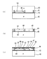
このような半導体圧力センサの製造に用いる半導体基板として、上述した圧力基準室に相当する部分をあらかじめ形成したものが供されている。これは、例えば、図19に示すように、2枚のシリコン基板を用いて貼り合わせ技術により圧力基準室を形成する方法である。
【0004】
すなわち、まず、同図(a)に示すように、第1のシリコン基板1にエッチングなどの方法により圧力基準室用の凹部2を形成し、第2のシリコン基板3の表面に酸化膜4を形成した状態で、第1のシリコン基板1の凹部2が第2のシリコン基板3の酸化膜4を形成した面により閉塞されるように密着させて貼り合わせる。このとき、貼り合わせは、真空中にて行なわれる。これによって、貼り合わせた状態では、凹部2が閉塞されて圧力基準室5として形成され内部は真空状態となる(同図(b)参照)。
【0005】
次に、第1のシリコン基板1側の露出している面を研磨することにより圧力基準室5の底面部の肉厚を所望の厚さ寸法に形成してダイヤフラム6となる部分を形成する。この後、ダイヤフラム6部分にピエゾ抵抗効果を有する抵抗体を複数個形成してそれらをブリッジ接続した状態とすることにより半導体圧力センサが形成される。
【0006】
これにより、半導体圧力センサ本体が置かれている環境の圧力がダイヤフラム6に作用すると、圧力基準室5内部との圧力差に応じた力でダイヤフラム6が変位し、抵抗体の抵抗値がピエゾ抵抗効果により変化するようになる。すると、ブリッジ回路の出力端子に圧力に応じた電圧が出力されるようになるので、これを検出すれば圧力を検出することができる。
【0007】
ところで、このような半導体圧力センサは、ダイヤフラム6にかかる圧力を、その応力で変化する抵抗体の抵抗値の変化として検出する原理であるから、ダイヤフラム6の厚さ寸法つまり、圧力に応じて変化する度合いが検出精度を決定する要素となる。つまり、ダイヤフラム6を薄く形成すれば、その分だけ検出精度を向上させることができるのである。また、逆に、検出精度を低下させることなくダイヤフラム6の面積を小さくするためには、ダイヤフラム6の厚さ寸法を薄くする必要がある。
【0008】
ところが、上述したような半導体基板の製造方法では、原理的に、内部が真空状態に近い圧力基準室5を形成した後にダイヤフラム6部分を形成するための研磨工程を実施せざるを得ないため、ダイヤフラム6の厚さを薄く(例えば1〜10μm程度)するように研磨を進めると、場合によっては、図17(c)に示すように、研磨途中で圧力基準室5内と外部との圧力差でダイヤフラム6部分が応力を受けて変形してしまうことがある。
【0009】
上述のような製造工程を経てダイヤフラムを形成する際に、そのとき研磨工程中に発生するダイヤフラム部分の変形が無視できない程度の大きさになる場合には、形成されるダイヤフラム6の厚さ寸法が全体として不均一になり、このことに起因して圧力に応じた変位の精度が低下したり、場合によっては、ダイヤフラム6の中央部が圧力基準室5内で接触した状態となってそれ以上の変位が妨げられてしまうような状態になる不具合がある。
【0010】
本発明は、上記事情に鑑みてなされたもので、その目的は、圧力基準室の背面部のダイヤフラム部分の厚さを薄くする加工を行なう場合でも、その加工工程の途中に圧力基準室内外の圧力差で受ける変形応力に起因して圧力測定に悪影響を及ぼすことを無くすることができる半導体基板の製造方法を提供することにある。
【0011】
【課題を解決するための手段】
請求項1の発明によれば、凹部形成工程で第1の基板に凹部を形成し、次の貼り合わせ工程でこれを大気圧相当の雰囲気中で第2の基板と貼り合わせることにより圧力基準室の形状を形成し、この後、減圧工程にて圧力基準室内を減圧するようにしているので、貼り合わせ工程を減圧した雰囲気中で行なう必要がなく、これによって貼り合わせ工程を簡単且つ容易に行なうことができ、しかも、減圧工程を実施する前に圧力基準室の形成される部分の基板の厚さを研磨などにより加工したり、あるいは素子を形成する工程を実施する際に内部の圧力との差で変形するなどの不具合が発生することがないので、精度の良い加工を行なうことができるようになる。
【0014】
また、貼り合わせ工程では、圧力基準室用の凹部内を外部と隔絶するように密閉状態とし、さらに、減圧工程では、熱処理を行なうことで、圧力基準室用の凹部内の気体を基板部材と化合させることにより消費させ、これによって内部を減圧するようにしたので、簡単且つ確実に圧力基準室を減圧した状態に形成することができるようになる。
そして、研磨工程を減圧工程の前に実施するので、圧力基準室用の凹部が形成された部分の基板を研磨してダイヤフラム形成部を設ける場合に、内外の圧力差による応力で研磨中にダイヤフラム形成部が変形するといったことがなくなり、圧力センサなどに用いるダイヤフラムを精度良く加工形成することができるようになる。
そして、請求項2の発明によれば、圧力基準室用の凹部内に残存する酸素を基板部材と化合させて酸化物を生成することにより減圧するので、特殊な反応物質などを用いることなく簡単且つ安価に成し得る。
【0015】
請求項3の発明によれば、上述の反応が促進するように、あらかじめ圧力基準室用の凹部内を半導体面が露出するように表面処理しておくので、効率的に減圧工程を実施することができるようになる。そして、請求項4の発明によれば、その表面処理として、酸化膜を除去することにより、圧力基準室用の凹部内の酸素を消費しやすくするので、確実且つ迅速に減圧工程を実施させることができるようになる。
【0022】
【発明の実施の形態】
(第1の実施形態)
以下、本発明の第1の実施形態について図1ないし図6を参照しながら説明する。
図1は、本発明の半導体基板の製造方法を適用して作製した半導体基板11を用いて形成した半導体圧力センサのセンサチップ12の断面構造を模式的に示すもので、図2はその上面図を示すものである。
【0023】
第1の基板としての単結晶シリコン基板13には、酸化膜14を介して下面側に第2の基板としてのベースシリコン基板15が貼り付けられている。単結晶シリコン基板13の下面側中央部には圧力基準室16が外部と隔絶された状態に形成され、内部は略真空となるようにガスが排気されている。また、圧力基準室16は単結晶シリコン基板13の側面に延びるように形成された連通孔17と連通した状態に形成されており、その連通孔17は途中で上方から形成された封止孔18の部分で酸化膜19により封止されている。
【0024】
圧力基準室16の上面は、所定の厚さ寸法まで研磨されたダイヤフラム20として設けられている。このダイヤフラム20は、外部の圧力に応じて変位する程度の厚さ寸法に設定されており、そのダイヤフラム20部分にはピエゾ抵抗効果を有する4つの抵抗体21が拡散などの方法により形成されている。各抵抗体21にはオーミックコンタクトをとるための高不純物濃度領域22が形成されている。この高不純物濃度領域22の表面のコンタクト領域を除いて基板の全面に絶縁膜としての酸化膜23が形成されている。
【0025】
この上面には、4つの抵抗体21をブリッジ接続するようにアルミニウム電極パターン24が形成されており、それらの端部にはボンディングパッド24aが形成されている。そして、このボンディングパッド24a部分を除いた全面に、保護用で上述した封止を行なったと同じ酸化膜19が配設されている。このような構成としたセンサチップ12は、図示しないボンディングワイヤによりボンディングパッド24a部分で外部回路に接続された状態で使用される。これによってブリッジ回路に外部から電圧が印加されると共に、検出出力が外部に導出できる。
【0026】
そして、このセンサチップ12を圧力測定の環境下にさらすと、ダイヤフラム20が外部から受ける圧力で圧力基準室16内の圧力との差により生ずる応力で変位するので、抵抗体21はピエゾ抵抗効果で抵抗値が変化するようになる。この抵抗値の変化を検出出力として圧力に応じた電圧信号を得ることができるようになる。この場合、圧力基準室16は略真空状態つまり気体が存在しない状態に設けられているので、温度が変動してもその温度変動に応じて内部の圧力が変動することがほとんどないので、温度補償回路などを設けることなく、正確な圧力を検出することができるようになるものである。
【0027】
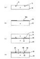
次に、上述のセンサチップ12の製造方法について、図3ないし図6も参照して説明する。図3は、概略的な製造工程を説明する流れ図で、以下、この製造工程にしたがって説明する。
まず、酸化膜形成工程P1では、第1の基板である単結晶シリコン基板13の表面に熱酸化などの方法により酸化膜25を形成する(図4(a)参照)。この場合、酸化膜25の膜厚は、例えば、0.1〜1.0μm程度である。なお、この酸化膜25は、熱酸化以外にCVD法などにより形成することもできる。
【0028】
次に、連通孔形成工程P2では、単結晶シリコン基板13の酸化膜25の一部をフォトリソグラフィ処理によって開口し(同図(b)参照)、露出した部分の単結晶シリコン基板13をフッ素イオンなどによるドライエッチング処理により連通孔17を設けるための凹部13aを形成する(同図(c)参照)。凹部13aの大きさは、例えば、開口部が50〜1000μm程度の寸法で、深さが10μm程度以下に形成している。
【0029】
この場合、エッチング処理は、KOH(水酸化カリウム)液あるいはTMAH(テトラメチルアンモニア水溶液)などを用いたウェットエッチング処理を適用することもできる。続いて、圧力基準室用凹部形成工程P3では、同様にしてフォトリソグラフィ処理によって酸化膜25に開口部を形成し、露出した単結晶シリコン基板13の部分をエッチングにより除去して圧力基準室16用の凹部13bを形成する(同図(d)参照)。
【0030】
この後、酸化膜除去工程P4では、単結晶シリコン基板13の表面に形成されている酸化膜25をエッチング処理により除去した状態とする。なお、このように酸化膜25を除去するのは、次の貼り合わせ工程P5で、単結晶シリコン基板13に反りが生じている場合に貼り合わせ不良が発生するのを防止するためである。第2の基板としてのベースシリコン基板15に対して、別途に酸化膜形成工程P1aにて、表面に酸化膜14を形成する(図5(a)参照)。
【0031】
次に、貼り合わせ工程P5では、単結晶シリコン基板13およびベースシリコン基板15をそれぞれ前処理を行なった後に、単結晶シリコン基板13の圧力基準室用の凹部13bを形成した面側とベースシリコン基板15の酸化膜14を形成した面側とを、大気圧中において密着させるようにして貼り合わせ(同図(b)参照)、続けて熱処理を行なう(熱処理温度は800℃〜1150℃の範囲で、低温の場合には最高3時間程度、高温の場合には最低0.5時間程度の熱処理を行なう)。これにより、貼り合わせた基板の内部に圧力基準室16が形成されるが、この状態では、連通孔17により外部と連通した状態となっているので、圧力基準室16内は大気圧のままである。
【0032】
そして、研磨工程P6では、この状態で、単結晶シリコン基板13の上面側を研磨して、圧力基準室用凹部13bの上部に位置する部分をダイヤフラム20として形成する(同図(c)参照)。このとき、研磨により調整するダイヤフラム20の厚さ寸法は、例えば、1〜10μm程度である。なお、このとき、圧力基準室16内は上述同様に大気圧に保持されているので、研磨によってダイヤフラム20の部分の厚さが薄くなっても、圧力差によって撓むことがないので、均一な厚さ寸法に研磨することができる。
【0033】
そして、上述のようにして形成された状態で、センサチップ12としての機能を達成させるための素子を形成する素子形成工程P7を実施する。この場合においては、ダイヤフラム20の部分にピエゾ抵抗効果を有する抵抗体21を拡散法などの周知の技術を用いて不純物を導入することにより形成し、この後、抵抗体21とオーミック接触が取れるように高濃度不純物領域22を形成する(図6(a)参照)。
【0034】
次に、封止孔形成工程P8では、単結晶シリコン基板13の上面側から封止孔18を形成する。単結晶シリコン基板13の上面に前述同様のフォトリソグラフィ処理を施して封止孔18に対応した部分のシリコン面を露出させ、エッチング処理により下方に向けてエッチングを行なって連通孔17の位置まで掘り下げて封止孔18を形成する(同図(b)参照)。
【0035】
この後、減圧工程としての封止工程P9にて、真空中で単結晶シリコン基板13の上面全面に酸化膜19を形成する(同図(c)参照)。これにより、封止孔18部分にも酸化膜19が形成され、連通孔17部分を封止するようになり、圧力基準室16内が真空状態に形成される。この場合、圧力基準室16内の圧力は、例えば、真空状態の程度として100Pa(パスカル)以下程度とすることが好ましく、さらに低い圧力に設定することは検出精度の向上につながる。なお、酸化膜19に代えて、シリコン窒化膜などを形成することもできる。
【0036】
最後に、電極パッド部開口処理工程P10にて、アルミニウム電極パターン24のボンディングパッド24a部分の酸化膜19をフォトリソグラフィ処理により開口すると、図1および図2に示すような構成のセンサチップ12を得ることができる。
【0037】
このような本実施形態によれば、ダイヤフラム20を形成してから(研磨工程P6を実施してから)圧力基準室16内部を減圧する封止工程P7を実施するので、研磨中に圧力基準室16内外の圧力差によるダイヤフラム20の撓みが発生するのを防止でき、これによって、ダイヤフラム20の膜厚を均一に精度良く形成することができる。
【0038】
また、本実施形態によれば、上述のごとくダイヤフラム20の厚さ寸法を薄く形成することができるので、ダイヤフラム20部分の面積を小さくすることにより検出精度の低下を招くのを防止できるようになり、素子の小形化を図ることができるようになる。
【0039】
さらに、本実施形態によれば、連通孔17を形成しておいて素子形成工程P7を経た後に封止工程P9にて真空中で封止孔18を封止することにより圧力基準室15内を真空に減圧するので、内部を確実に減圧することができると共に、その真空度の設定も確実に行なうことができる。
【0040】
(第2の実施形態)
図7ないし図12は本発明の第2の実施形態を示すもので、以下、第1の実施形態と異なる点について説明する。図7は、半導体基板26を用いて形成した半導体圧力センサのセンサチップ27の断面構造を模式的に示すもので、図2はその上面図を示すものである。
【0041】
第1の基板としての単結晶シリコン基板28は、酸化膜29を介して下面側に第2の基板としてのベースシリコン基板30が貼り付けられた状態とされている。単結晶シリコン基板28の下面側中央部には圧力基準室31が外部と隔絶された状態に形成されており、内部は略真空状態となるように脱気されている。また、後述するように、脱気される過程で形成される酸化膜31aが内壁面に設けられている。
【0042】
圧力基準室31の上面には、所定の厚さ寸法のダイヤフラム32が形成されている。ダイヤフラム32は、外部の圧力に応じて変位する程度の厚さ寸法に設定されており、そのダイヤフラム32部分には、前述同様にして4つの抵抗体33および高不純物濃度領域34が形成されている。この高不純物濃度領域34のコンタクト領域を除いて全面に絶縁膜としての酸化膜35が形成されている。4つの抵抗体21をブリッジ接続するアルミニウム電極パターン36は、端部にボンディングパッド36aが形成されている。そして、このボンディングパッド36a部分を除いた全面に、保護用の酸化膜37が配設されている。
【0043】
次に、上述のセンサチップ27の製造方法について、図9ないし図12も参照して説明する。図9に示す概略工程にしたがって、まず、酸化膜形成工程T1では、第1の基板である単結晶シリコン基板28の表面に熱酸化などの方法により酸化膜38を形成する(図10(a)参照)。次に、圧力基準室用凹部形成工程T2では、単結晶シリコン基板28の酸化膜38の一部をフォトリソグラフィ処理によって開口し(同図(b)参照)、露出した部分をエッチングにより除去して圧力基準室31用の凹部28aを形成する(同図(c)参照)。
【0044】
この後、酸化膜除去工程T3では、単結晶シリコン基板28の表面に形成されている酸化膜38をエッチング処理により除去した状態とする。なお、このように酸化膜38を除去するのは、後の減圧工程T6で圧力基準室31用の凹部28a内の脱気が効率良く行なわれるようにするためと、単結晶シリコン基板28の反りによる貼り合わせ不良を防止するためである。第2の基板としてのベースシリコン基板30に対して、別途に酸化膜形成工程T1aにて、表面に酸化膜29を形成する(図11(a)参照)。
【0045】
次に、貼り合わせ工程T4では、単結晶シリコン基板28およびベースシリコン基板30をそれぞれ前処理を行なった後に大気圧中において密着させるように貼り合わせ(同図(b)参照)、続けて熱処理を行なう(熱処理温度は800℃〜1150℃の範囲で、低温の場合には最高3時間程度、高温の場合には最低0.5時間程度の熱処理を行なう)。これにより、貼り合わせた基板の内部に圧力基準室31が形成されるが、この状態では、内部は大気圧のままである。
【0046】
そして、研磨工程T5では、この状態で、単結晶シリコン基板28の上面側を研磨して、圧力基準室用凹部28aの上部に位置する部分をダイヤフラム32として形成する(同図(c)参照)。なお、このとき、研磨により調整するダイヤフラム20の厚さ寸法は、例えば、1〜10μm程度であり、圧力基準室31内は上述同様に大気圧に保持されているので、研磨によってダイヤフラム32の部分の厚さが薄くなっても、圧力差によって撓むことがないので、均一な厚さ寸法に研磨することができる。
【0047】
そして、次に減圧工程としての酸化膜形成工程T6を実施する。これは、例えば1150℃〜1200℃程度の範囲内で0.5時間から5時間の範囲で熱処理を行なう。これにより、圧力基準室31内では、内部に残留している酸素が内壁を構成するシリコンと化合して酸化膜31aとして消費され、内部の圧力がほぼ真空レベルとなるまで低下するようになる(図12(a)参照)。また、このとき、単結晶シリコン基板28の上面にも同様にして酸化膜39が形成される。
【0048】
次に、表面酸化膜除去工程T7では、上述の工程で形成された酸化膜39を除去し、続く酸化膜形成工程T8にて、新たに酸化膜40を形成し、半導体基板26が完成する。この後、ダイヤフラム32部分に前述同様にしてセンサチップ27として機能するようにピエゾ抵抗効果を有する抵抗体33およびオーミック接触用の高濃度不純物領域34を形成すると共に、アルミニウム電極パターン36を形成して図7に示すセンサチップ27が形成される。
【0049】
このような第2の実施形態によれば、酸化膜31aを形成するように熱処理を行なって、圧力基準室31内の残留酸素を消費して内部を減圧するので、工程が簡単で、且つ確実に内部を減圧することができ、これによって、研磨工程では圧力基準室31内を大気圧に保持した状態で研磨を行なえ、ダイヤフラム32の膜厚を精度良く形成することができる。
【0050】
(第3の実施形態)
図13ないし図15は本発明の第3の実施形態を示すもので、第1および第2の実施形態と異なるところは、圧力センサ素子に加えてその信号処理回路としての集積回路部を一体に形成した圧力検出用センサチップ41を構成したところである。また、この圧力検出用センサチップ41の製造方法においては、第1および第2の実施形態と異なり、貼り合わせ工程においては真空中で行なう方法を採用すると共に、その後、研磨工程を経てダイヤフラムを形成するようにしているものである。
【0051】
そこで、本実施形態においては、従来例の説明において述べたような不具合が発生するのを抑制するために、形成しようとしているダイヤフラムの厚さ寸法を後述する関係の条件式を満たすように設定しているものである。
【0052】
図13は本発明でいうところの半導体装置である圧力検出用センサチップ41の全体構成を模式的な断面で示しており、図14は平面図を示している。これらの図13,図14において、支持基板としてのp型のベースシリコン基板42上には絶縁用の酸化膜43が形成されると共に半導体層としての素子形成領域44,45が形成されている。素子形成領域44は圧力センサ素子46が形成される領域として設けられ、素子形成領域45は集積回路部47が形成される領域として設けられており、これらの間はトレンチ分離構造として機能する研磨ストッパ用のシリコン酸化膜48により電気的に絶縁した状態に分離形成されている。
【0053】
また、素子形成領域44および45を構成する単結晶シリコン膜は、後述するようにして貼り合わせ技術を用いて形成されるが、n型不純物を導入した層として設けられ、例えば、数μmから20μm程度の比較的厚い膜厚となるように形成されている。
【0054】
素子形成領域44において、下面側の酸化膜43と接する部分には、エッチングにより所定形状で所定深さに凹部49が形成されており、この凹部49の開口部分は酸化膜43により閉塞され、これによって内部に圧力基準室50が設けられている。また、この圧力基準室50内は、真空あるいは所定の減圧圧力に設定されており、圧力測定時に温度変動によらない基準圧力として機能するようになっている。また、この圧力基準室50を設けることにより、その表面側のn型層部分が圧力測定に必要とされる所定膜厚に設定されたダイヤフラム51として機能するように設けられている。
【0055】
ダイヤフラム51には、圧力基準室50の縁部と対応する位置の表面部分に圧力測定用の抵抗体領域52が4個形成されている。これらは、前述同様にしてピエゾ抵抗効果を利用して圧力に応じてダイヤフラム51が変形すると、これを抵抗値の変化として検出するように設けられたものである。そして、素子形成領域44の表面には、酸化膜53が形成されており、抵抗体領域52に対応して開口部が形成され、この部分を介してアルミニウム電極膜54によりブリッジ接続された状態に構成されている。
【0056】
一方、素子形成領域45には、種々の素子が形成されて集積回路部47が構成されるが、例えば、図13に示すものでは、バイポーラ型のトランジスタ55が形成されている。このトランジスタ55は、n型の素子形成領域45をコレクタ領域としてp型のベース領域56,n型のエミッタ領域57およびn型のコンタクト領域58を形成してなるもので、全体を覆う酸化膜53は、ベース領域56,エミッタ領域57およびコレクタのコンタクト領域58に対応して開口された部分を介してアルミニウム電極膜54により電気的に接続されており、他の回路素子と接続されている。
【0057】
なお、図示はしないが、他にMOSFETやダイオード,抵抗体などの種々の回路素子が形成されて圧力検出回路などの集積回路部47が形成されている。また、この集積回路部47の外周部は、前述したように研磨ストッパを兼ねたトレンチ構造のシリコン酸化膜48により囲まれるようにして圧力センサ46とは分離されており、圧力センサ46の領域は、このシリコン酸化膜48により集積回路部47とは絶縁分離される。また、圧力検出用センサチップ41の表面全体には図示しないボンディングパッド部分を除いて保護膜59が形成されている。
【0058】
上記構成において、ダイヤフラム51の膜厚h(mm)は、次のようにして得られる条件を満足するように設定されている。すなわち、周囲が固定された板材に受ける圧力で撓む量を求める場合において定義される式は、撓み量の最大値をw(mm),板材の厚さ寸法h(mm),板材に受ける圧力をP(kgf/mm2),材料の弾性率をE(kgfmm2)とした場合に、次式(A)で与えられる。
w=α×(P×a4)/(E×h3) …(A)
ここで、αは、板材の平面的な形状に起因した係数である。
【0059】
そこで、本実施形態における圧力センサ部44について当てはめてみると、ダイヤフラム51の平面形状は一辺の長さ寸法がa(mm)の正方形状であるから、上述の式(A)中のαの値は0.014として与えられる。これにより、上式(A)は、
w=0.014×(P×a4)/(E×h3) …(B)
となる。
【0060】
また、ダイヤフラム51が受ける圧力をP(kgf/mm2)とすると、これは受圧面側から受ける圧力Poから圧力基準室50内の基準圧力(減圧もしくは真空状態)Psを差し引いた値として与えられるから、例えば、Psを真空つまり0kgf/mm2とした場合には、PはPoに等しくなる。したがって、通常の状態で受ける圧力として1気圧を想定すると、1.033×10−2kgf/mm2となる。さらに、ダイヤフラム51は、単結晶シリコンで構成されるから、弾性率Eは、17000kgf/mm2となる。
【0061】
ここで、上述の式(B)で得られる撓み量の最大値wが、ダイヤフラム51の厚さ寸法を設定する際に、実質的に悪影響を受けない程度を想定すると、最大でもダイヤフラム51の厚さ寸法以下程度となれば良いから、式(B)において、この条件を考慮すると、
w=0.014×(P×a4)/(E×h3)>h …(C)
という条件式(C)が満たされれば良いことになる。
【0062】
そこで、上述の条件式(C)に上述したP,Eの具体的な値を代入すると、この条件式を満たす関係としてダイヤフラム51の一辺の長さ寸法aの厚さ寸法hに対する比の値(a/h)の値についての条件を求めることができ、
(a/h)<104 …(D)
という関係を得ることができる。すなわち、ダイヤフラム51の一辺の長さ寸法aに対して条件式(D)を満たす厚さ寸法hに設定すれば撓み量の最大値wをその厚さ寸法hよりも小さい程度に抑制することができるようになるのである。この場合では、例えば、ダイヤフラム51の厚さ寸法hを2μm程度に設定する場合には、一辺の長さ寸法aを208μmよりも小さい寸法に設定すれば良いということになる。
【0063】
次に、上述の圧力検出用センサチップ41の製造方法について、図15および図16に示す概略的な製造工程に対応した断面図も参照して説明する。
この実施形態においては、半導体層用基板として図15(a)に示すように、n型不純物が導入された単結晶シリコン基板60を用いている。まず、トレンチ形成工程において、半導体基板60の表面に、素子分離領域44,45に対応して設けるシリコン酸化膜48を配設するためのトレンチ61を所定深さ寸法に形成する。このトレンチ61は、前述したように圧力センサ素子46と集積回路部47とを絶縁分離すると共に、後工程においてダイヤフラム51を形成する際の研磨工程での研磨ストッパとしての機能も兼ねたものである。
【0064】
さて、トレンチ形成工程では、具体的には、半導体基板60の表面にPE−CVD TEOS(plasma enhanced chemical vapor deposition tetralxy ortho silicate )膜などの酸化膜をエッチングのマスク部材として所定膜厚だけデポジションし、続いてトレンチ61を形成する部分をフォトリソグラフィ処理によって開口する。この後、ドライエッチング処理などの方法によって異方性エッチングを行ない、PE−CVD TEOSによる酸化膜をエッチングすると共に、シリコンをエッチングして所定深さ寸法のトレンチ61を形成する。
【0065】
次に、酸化膜形成工程では、トレンチ61内の表面にシリコン酸化膜48を形成すると共に、半導体基板60の表面にシリコン酸化膜62を形成するもので、具体的には、LP−HTO(low pressure high temperature oxide )法などの熱酸化により形成し、半導体基板62の表面を平坦な状態にする.次に、圧力基準室50を形成するための領域の表面の酸化膜62を除去して開口部を形成し、ここを介して所定深さまでp型不純物を導入してp型領域63を形成する(同図(b)参照)。
【0066】
続いて、圧力基準室用凹部形成工程では、p型領域63を選択的にエッチングして除去する(同図(c)参照)。この場合、p型領域63のみを選択的にエッチングする方法としては、pn接合部分に逆バイアスを印加した状態でエッチング液に浸して行なう電気化学ストップエッチング法がある。この方法を用いると、p型領域63部分のエッチングがほぼ完了すると、pn接合が無くなることにより電流が流れるようになり、陽極酸化膜を形成するようになる。これによってシリコンの層が陽極酸化膜に変わると、シリコンの露出がなくなってエッチングが停止する。この結果、p型領域63部分をエッチングにより除去して凹部49を形成することができる。
【0067】
なお、上述の場合で、圧力基準室用凹部49の形成は、p型領域63を形成して電気化学ストップエッチングにより形成することに代えて、通常のドライエッチング処理などにより所定深さ寸法の凹部49を形成するようにしても良い。
【0068】
一方、支持基板として用いる単結晶シリコンからなるベースシリコン基板42には、酸化膜形成工程において、表面に所定の膜厚で熱酸化などの方法により酸化膜43が形成される(同図(d)参照)。この酸化膜43は、前述したように、半導体層44,45に対する絶縁膜として機能するものである。
【0069】
次に、貼り合わせ工程においては、ベースシリコン基板42および半導体基板62のそれぞれに対して、所定の前処理工程を実施して表面を貼り合わせするのに適した状態とした後に、減圧雰囲気として真空中にてベースシリコン基板42の酸化膜43の面と半導体基板62の凹部49を形成した側の面とを貼り合わせる(図16(a)参照)。この後、熱処理を行なって貼り合わせ面の密着強度を高める。
【0070】
そして、研磨工程では、単結晶シリコン基板62の上面側を研磨して、圧力基準室用凹部49の上部に位置する部分をダイヤフラム51として形成する(同図(b)参照)。このとき、研磨により調整するダイヤフラム51の厚さ寸法は、例えば、1〜10μm程度であるが、前述した条件を満たすように設定されている。したがって、研磨によってダイヤフラム51の部分の厚さが薄くなっても、そのときの圧力差Pによってダイヤフラム51の撓み量の最大値wは、ダイヤフラム51の厚さ寸法h以上となることがないので、ほぼ均一な厚さ寸法に研磨することができる。
【0071】
そして、上述のようにして形成された状態で、センサチップ41としての機能を達成させるための素子を形成する素子形成工程を実施する。この場合においては、ダイヤフラム51の部分にピエゾ抵抗効果を有する抵抗体52を拡散法などの周知の技術を用いて不純物を導入することにより形成し、さらには、集積回路部47としてのバイポーラトランジスタ55を構成するベース領域56,エミッタ領域57およびコンタクト領域58などを形成する(同図(c)参照)。
【0072】
最後に、電極パッド部開口処理工程にて、アルミニウム電極パターン54のボンディングパッド部分の酸化膜59をフォトリソグラフィ処理により開口することにより、図13および図14に示すような構成のセンサチップ41を得ることができる。
【0073】
このような本実施形態によれば、ダイヤフラム51の厚さ寸hを、式(D)で示す条件を満たすように設定しているので、圧力基準室50を真空雰囲気中で貼り合わせを行なって形成し、ダイヤフラム51形成のための研磨工程を実施する場合でも、研磨の進行に伴うダイヤフラム51部分の撓み量wを抑制することができ、変形に伴う膜厚の不均一の発生を防止することができるようになる。
【0074】
また、本実施形態によれば、圧力検出用センサチップ41に圧力センサ素子46と集積回路部47を一体に設ける構成とすることができるので、圧力センサ素子46の検出出力に信号処理を行なった状態で出力信号として得ることができるようになる。この場合、通常の圧力センサ素子46に必要なダイヤフラム51の厚さ寸法hに対して、集積回路部47に形成する素子は深い寸法が必要となるのに対応して、圧力基準室50を凹部49を形成することにより設ける構成としているので、集積回路部47を形成するための設計の自由度を高めたものとすることができるようになる。
【0075】
(第4の実施形態)
図17および図18は、本発明の第4の実施形態を示すもので、第3の実施形態と異なるところは、集積回路部47を設けない圧力センサ部46のみを設けるディスクリート素子構造としたものであり、圧力基準室用の凹部をシリコンのエッチングで形成しないで圧力基準室を設けるようにしたところである。
【0076】
すなわち、半導体圧力センサチップ64は、支持基板としてのp型ベースシリコン基板65上には圧力基準室形成用の酸化膜66が所定膜厚で形成されており、その一部を正方形状に開口した圧力基準室67が形成されている。この圧力基準室67上には、単結晶シリコンからなる所定の厚さ寸法hを有するダイヤフラム68が設けられている。このダイヤフラム68は、周囲をトレンチ構造を有する酸化膜部69により区画されている。
【0077】
ダイヤフラム68には、圧力基準室67の縁部と対応する位置の表面部分に圧力測定用の抵抗体領域70が形成されている。これらは、前述同様にしてピエゾ抵抗効果を利用して圧力に応じてダイヤフラム68が変形すると、これを抵抗値の変化として検出するように設けられたものである。このダイヤフラム68の表面には、酸化膜71が形成されており、抵抗体領域70に対応して開口部が形成され、この部分を介してアルミニウム電極膜72によりブリッジ接続された状態に構成されている。また、表面全体にはボンディングパッド部分を除いた保護膜73が形成されている。
【0078】
上記構成において、ダイヤフラム68の膜厚h(mm)は、第3の実施形態と同様の条件を満足するように設定されている。すなわち、前述の式(A)からこのダイヤフラム68に対応して導かれる式(B)で得られる撓み量の最大値wが、前述同様の条件下でダイヤフラム68の厚さ寸法hよりも小となる条件として示される式(C)に当てはめると、式(D)で示す条件が得られる。すなわち、ダイヤフラム68の一辺の長さ寸法aに対して条件式(D)を満たす厚さ寸法hに設定すれば撓み量の最大値wをその厚さ寸法hよりも小さい程度に抑制することができるようになるのである。この場合では、例えば、ダイヤフラム51の厚さ寸法hを2μm程度に設定する場合には、一辺の長さ寸法aを208μmよりも小さい寸法に設定すれば良いということになる。
【0079】
次に、上述の圧力検出用センサチップ64の製造方法について、図18を参照して説明する。この実施形態においては、半導体層用基板として図18(a)に示すように、n型不純物が導入された単結晶シリコン基板74を用いている。まず、トレンチ形成工程において、半導体基板74の表面に、ダイヤフラム68部分に対応して設けるシリコン酸化膜69を配設するためのトレンチ75を所定深さ寸法に形成する。このトレンチ75は、後工程においてダイヤフラ68を形成するために行なう研磨工程での研磨ストッパとしての機能を果すように設けたものである。
【0080】
次に、支持基板として用いる単結晶シリコンからなるベースシリコン基板65には、酸化膜形成工程において、表面に所定の膜厚で熱酸化などの方法により酸化膜66が形成される(同図(b)参照)。この酸化膜66には、圧力基準室67に対応する部分にフォトリソグラフィ処理により正方形状をなす開口部66aが形成される。
【0081】
次に、貼り合わせ工程においては、ベースシリコン基板65および半導体基板74のそれぞれに対して、所定の前処理工程を実施して表面を貼り合わせするのに適した状態とした後に、真空中にてベースシリコン基板65の酸化膜66の面と半導体基板74のトレンチ75を形成した側の面とを貼り合わせる(同図(c)参照)。この後、熱処理を行なって貼り合わせ面の密着強度を高める。これにより、酸化膜66の開口部66a部分には、酸化膜66の厚さ寸法分だけの空間が形成され、これが圧力基準室67として得られるようになる。
【0082】
そして、研磨工程では、単結晶シリコン基板74の上面側を研磨して、圧力基準室用凹部67の上部に位置する部分をダイヤフラム68として形成する(同図(b)参照)。このとき、研磨により調整するダイヤフラム68の厚さ寸法は、例えば、1〜10μm程度であるが、前述した条件を満たすように設定されている。したがって、研磨によってダイヤフラム68の部分の厚さが薄くなっても、そのときの圧力差Pによってダイヤフラム68の撓み量の最大値wは、ダイヤフラム68の厚さ寸法h以上となることがないので、ほぼ均一な厚さ寸法に研磨することができる。
【0083】
そして、上述のようにして形成された状態で、センサチップ64としての機能を達成させるための素子を形成する素子形成工程を実施する。この場合においては、ダイヤフラム68の部分にピエゾ抵抗効果を有する抵抗体70を拡散法などの周知の技術を用いて不純物を導入することにより形成し、電極パッド部開口処理工程にて、アルミニウム電極パターン72のボンディングパッド部分の酸化膜71をフォトリソグラフィ処理により開口することにより、図17に示すような構成のセンサチップ64を得ることができる。
【0084】
このような本実施形態によれば、第3の実施形態と同様にして、圧力基準室67を真空中で貼り合わせ工程を実施することにより設けると共に、ダイヤフラム68の厚さ寸法hを前述の条件式(D)を満たすように設定して研磨工程を行なうので、撓み量の最大値wを抑制して素子形成や圧力測定に支障を来すことのないようにすることができるので、加工処理を簡略化することができる。
【0085】
また、本実施形態によれば、圧力基準室67を酸化膜66に開口部66aを形成することにより、貼り合わせ時にその部分が空間となるようにして設ける構成としたので、圧力基準室67を形成するために凹部を別途に加工形成する必要がなくなり、製造工程の簡略化を図ることができるようになる。
【0086】
本発明は、上記実施例にのみ限定されるものではなく、次のように変形また拡張できる。
研磨工程で発生することが予想されるダイヤフラムの撓みの度合いは、ダイヤフラムの厚さ寸法のみに依存するのではなくその面積にも依存しており、例えば、ダイヤフラムの厚さが比較的厚い場合でも、面積が広くなると内外の圧力差で発生する撓みの度合いが大きくなる。したがって、本発明においても、第1および第2の実施形態で示したダイヤフラム20,32の厚さ寸法の場合のみならず、さらに厚く形成する場合でも、面積が大きくなると、十分にその効果を得ることができるようになる。
【0087】
第1の基板として単結晶シリコン基板13,28を用い、ダイヤフラム20,32部分にピエゾ抵抗効果を利用する抵抗体21,33を利用する構成の実施形態について説明したが、単結晶のシリコン基板を必要としない場合には多結晶あるいはアモルファスを基体とした基板を用いることができるし、あるいはシリコン以外の材質の基板を用いることもできる。
【0088】
また、第2の基板としてベースシリコン基板15,30を用いたが、単結晶シリコンの基板に限らず、第1の基板と貼り合わせが可能で、剛性を有するセラミック製の基板であれば何でも良い。
【0089】
第2の実施形態では、圧力基準室31内を減圧するために、内部の酸素を消費して酸化膜31aを形成するようにしたが、これに限らず、内部に窒素を充填した状態で貼り合わせ工程を実施しておいて窒化シリコン膜を形成することで内部の窒素を消費して減圧するようにしても良いし、他の方法により内部の気体を消費して減圧するようにしても良い。
【0090】
上記各実施形態においては、ダイヤフラムの形状を一辺がaの正方形状とするものについて説明したが、製造工程が複雑になったりあるいは測定結果の信号処理や構造的な制約がなければ、正方形状に限らず、長方形状あるいは円形状にすることもできる。この場合、ダイヤフラムは圧力基準室の平面形状によって決まるので、その圧力基準室の凹部の形成工程と密接な関係を有することになる。したがって、凹部の形成工程上で問題がなければ採用することができる。また、第4の実施形態のように、凹部を形成しないものにおいては、長方形状あるいは円形状のダイヤフラムを設けることは容易なものとなる。
【0091】
ところで、ダイヤフラムを円形状に形成する場合には、第3の実施形態あるいは第4の実施形態において説明した条件式は次のように変更される。すなわち、ダイヤフラムの膜厚h(mm)は、平面形状が半径aの円形状をなす場合には、式(A)で示される式は、αの値が異なることを除いて同じとなるから、
w=α×(P×a4)/(E×h3) …(A)
となる。そこで、ダイヤフラムの平面形状が半径aの円形状である場合のαの値は、0.171tosite与えられるから、式(B)は、
w=0.171×(P×a4)/(E×h3) …(B′)
となる。
【0092】
次に、前述同様にして、式(B)で得られる撓み量の最大値wが、ダイヤフラムの厚さ寸法を設定する際に、ダイヤフラムの厚さ寸法以下程度となる条件を考慮すると、
w=0.171×(P×a4)/(E×h3)>h …(C′)
という条件式(C)が得られるので、これに第3の実施形態で説明したP,Eの具体的な値を代入すると、この条件式を満たす関係としてダイヤフラムの半径寸法aの厚さ寸法hに対する比の値(a/h)の値についての条件を求めることができ、
(a/h)<56 …(E)
という関係を得ることができる。すなわち、ダイヤフラムの半径寸法aに対して条件式(E)を満たす厚さ寸法hに設定すれば撓み量の最大値wをその厚さ寸法hよりも小さい程度に抑制することができるようになるのである。
【図面の簡単な説明】
【図1】本発明の第1の実施形態を示す半導体圧力センサチップの模式的な断面図
【図2】半導体圧力センサチップの上面図
【図3】製造工程の概略を示す流れ図
【図4】製造工程別の模式的断面図(その1)
【図5】製造工程別の模式的断面図(その2)
【図6】製造工程別の模式的断面図(その3)
【図7】本発明の第2の実施形態を示す図1相当図
【図8】図2相当図
【図9】図3相当図
【図10】製造工程別の模式的断面図(その1)
【図11】製造工程別の模式的断面図(その2)
【図12】製造工程別の模式的断面図(その3)
【図13】本発明の第3の実施形態を示す図1相当図
【図14】図2相当図
【図15】製造工程別の模式的断面図(その1)
【図16】製造工程別の模式的断面図(その2)
【図17】本発明の第4の実施形態を示す図1相当図
【図18】製造工程別の模式的断面図
【図19】従来例を示す製造工程別の模式的断面図
【符号の説明】
11,26は半導体基板、12,27,41,64は半導体圧力センサチップ、13,28,42,65は単結晶シリコン基板(第1の基板)、14,29,43,66は酸化膜、15,30,62,74はベースシリコン基板(第2の基板)、16,31,50,67は圧力基準室、17は連通孔、18は封止孔、19は酸化膜、20,32,51,68はダイヤフラム、21,33,52,70は抵抗体、22,34は高不純物濃度領域、24,36,54,72はアルミニウム電極パターン、24a,36aはボンディングパッド、25,38は酸化膜、31aは酸化膜である。[0001]
BACKGROUND OF THE INVENTION
The present invention relates to a method of manufacturing a semiconductor substrate having therein a pressure reference chamber used for a pressure sensor or the likeTo the lawRelated.
[0002]
[Problems to be solved by the invention]
Some semiconductor pressure sensors that detect the pressure applied to the diaphragm have a pressure reference chamber inside. In this case, in order to improve detection accuracy, the pressure reference chamber reduces the amount of gas remaining inside as much as possible to reduce the fluctuation of the reference pressure due to the temperature fluctuation.
[0003]
As a semiconductor substrate used for manufacturing such a semiconductor pressure sensor, a substrate in which a portion corresponding to the pressure reference chamber described above is formed in advance is provided. For example, as shown in FIG. 19, a pressure reference chamber is formed by a bonding technique using two silicon substrates.
[0004]
That is, first, as shown in FIG. 2A, the
[0005]
Next, by polishing the exposed surface on the
[0006]
As a result, when the pressure of the environment in which the semiconductor pressure sensor body is placed acts on the
[0007]
By the way, such a semiconductor pressure sensor is based on the principle that the pressure applied to the
[0008]
However, in the semiconductor substrate manufacturing method as described above, in principle, after forming the
[0009]
When the diaphragm is formed through the manufacturing process as described above, if the deformation of the diaphragm portion generated during the polishing process is a size that cannot be ignored, the thickness dimension of the
[0010]
The present invention has been made in view of the above circumstances. The purpose of the present invention is to improve the pressure inside and outside of the pressure reference chamber in the middle of the processing step even when the thickness of the diaphragm portion on the back surface of the pressure reference chamber is reduced. Semiconductor substrate manufacturing method that can eliminate adverse effects on pressure measurement due to deformation stress caused by pressure differenceThe lawIt is to provide.
[0011]
[Means for Solving the Problems]
According to the first aspect of the present invention, a concave portion is formed on the first substrate in the concave portion forming step, and this is bonded to the second substrate in an atmosphere corresponding to atmospheric pressure in the next bonding step, thereby providing a pressure reference chamber. After that, the pressure reference chamber is depressurized in the depressurization step, so that it is not necessary to perform the bonding step in a reduced pressure atmosphere, thereby making the bonding step simple and easy. In addition, the thickness of the substrate in the portion where the pressure reference chamber is formed can be processed by polishing or the like before the decompression step is performed, or the internal pressure is reduced when the step of forming the device is performed. Since there is no problem such as deformation due to the difference, it is possible to perform highly accurate machining.
[0014]
Further, in the bonding step, the pressure reference chamber recess is hermetically sealed so as to be isolated from the outside. Further, in the decompression step, heat treatment is performed so that the gas in the pressure reference chamber recess is exchanged with the substrate member. Since they are consumed by combining them and the inside is decompressed, the pressure reference chamber can be formed in a decompressed state easily and reliably.
Since the polishing step is performed before the pressure reducing step, when the diaphragm forming portion is provided by polishing the substrate in which the concave portion for the pressure reference chamber is formed, the diaphragm is being polished by the stress due to the pressure difference between the inside and outside. The forming portion is not deformed, and the diaphragm used for the pressure sensor or the like can be processed and formed with high accuracy.
According to the second aspect of the present invention, since the oxygen remaining in the recess for the pressure reference chamber is combined with the substrate member to reduce the pressure by generating an oxide, it is easy to use without using a special reactant or the like. And it can be made inexpensively.
[0015]
Claim3According to the invention, the surface treatment is performed in advance so that the semiconductor surface is exposed in the recess for the pressure reference chamber so that the above-described reaction is promoted, so that the decompression step can be performed efficiently. become. And claims4According to the invention, as the surface treatment, by removing the oxide film, it becomes easy to consume oxygen in the recess for the pressure reference chamber, so that the depressurization step can be carried out surely and quickly. .
[0022]
DETAILED DESCRIPTION OF THE INVENTION
(First embodiment)
Hereinafter, a first embodiment of the present invention will be described with reference to FIGS.
FIG. 1 schematically shows a cross-sectional structure of a
[0023]
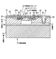
A
[0024]
The upper surface of the
[0025]
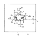
On this upper surface, an
[0026]
When the
[0027]
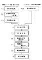
Next, a method for manufacturing the
First, in the oxide film forming step P1, an
[0028]
Next, in the communication hole forming step P2, a part of the
[0029]
In this case, a wet etching process using a KOH (potassium hydroxide) solution, TMAH (tetramethylammonia aqueous solution), or the like can be applied as the etching process. Subsequently, in the pressure reference chamber recess forming step P3, an opening is formed in the
[0030]
Thereafter, in the oxide film removing step P4, the
[0031]
Next, in the bonding step P5, the single
[0032]
In the polishing step P6, in this state, the upper surface side of the single
[0033]
And the element formation process P7 which forms the element for achieving the function as the
[0034]
Next, in the sealing hole forming step P <b> 8, the sealing
[0035]
Thereafter, in a sealing step P9 as a decompression step, an
[0036]
Finally, when the
[0037]
According to this embodiment, since the
[0038]
Further, according to the present embodiment, the thickness dimension of the
[0039]
Furthermore, according to the present embodiment, the
[0040]
(Second Embodiment)
FIGS. 7 to 12 show a second embodiment of the present invention, and differences from the first embodiment will be described below. FIG. 7 schematically shows a cross-sectional structure of the
[0041]
The single
[0042]
A
[0043]
Next, a method for manufacturing the
[0044]
Thereafter, in the oxide film removing step T3, the
[0045]
Next, in the bonding step T4, the single
[0046]
In the polishing step T5, in this state, the upper surface side of the single
[0047]
Then, an oxide film forming step T6 is performed as a decompression step. For example, the heat treatment is performed in a range of about 1150 ° C. to 1200 ° C. for 0.5 hours to 5 hours. As a result, in the
[0048]
Next, in the surface oxide film removal step T7, the
[0049]
According to the second embodiment, the heat treatment is performed so as to form the
[0050]
(Third embodiment)
FIGS. 13 to 15 show a third embodiment of the present invention. The difference from the first and second embodiments is that an integrated circuit portion as a signal processing circuit is integrated in addition to the pressure sensor element. The formed pressure
[0051]
Therefore, in this embodiment, in order to suppress the occurrence of the problems described in the description of the conventional example, the thickness dimension of the diaphragm to be formed is set so as to satisfy the conditional expression of the relationship described later. It is what.
[0052]
FIG. 13 shows a schematic cross section of the entire structure of a pressure detecting
[0053]
The single crystal silicon film constituting the
[0054]
In the
[0055]
In the
[0056]
On the other hand, in the
[0057]
Although not shown, various circuit elements such as MOSFETs, diodes, and resistors are formed to form an
[0058]
In the above configuration, the film thickness h (mm) of the
w = α × (P × a4) / (E × h3... (A)
Here, α is a coefficient resulting from the planar shape of the plate material.
[0059]
Therefore, when applied to the
w = 0.014 × (P × a4) / (E × h3) ... (B)
It becomes.
[0060]
The pressure received by the
[0061]
Here, assuming that the maximum value w of the deflection amount obtained by the above formula (B) is not substantially adversely affected when setting the thickness dimension of the
w = 0.014 × (P × a4) / (E × h3)> H (C)
It is sufficient that the conditional expression (C) is satisfied.
[0062]
Therefore, when the specific values of P and E described above are substituted into the conditional expression (C), the value of the ratio of the length dimension “a” of one side of the
(A / h) <104 (D)
Can be obtained. That is, if the thickness dimension h that satisfies the conditional expression (D) is set with respect to the length dimension a of one side of the
[0063]
Next, a method for manufacturing the above-described pressure detecting
In this embodiment, as shown in FIG. 15A, a single
[0064]
In the trench formation process, specifically, an oxide film such as a PE-CVD TEOS (plasma enhanced chemical vapor deposition tetralxy orthosilicate) film is deposited on the surface of the
[0065]
Next, in the oxide film forming step, the
[0066]
Subsequently, in the pressure reference chamber recess forming step, the p-
[0067]
In the above-described case, the pressure
[0068]
On the other hand, an
[0069]
Next, in the bonding process, a predetermined pretreatment process is performed on each of the
[0070]
In the polishing step, the upper surface side of the single
[0071]
And the element formation process which forms the element for achieving the function as the
[0072]
Finally, in the electrode pad portion opening processing step, the
[0073]
According to this embodiment, since the thickness dimension h of the
[0074]
Further, according to the present embodiment, since the
[0075]
(Fourth embodiment)
FIGS. 17 and 18 show a fourth embodiment of the present invention. The difference from the third embodiment is that a discrete element structure is provided in which only the
[0076]
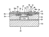
That is, in the semiconductor
[0077]
In the
[0078]
In the above configuration, the film thickness h (mm) of the
[0079]
Next, a method for manufacturing the pressure
[0080]
Next, an
[0081]
Next, in the bonding process, a predetermined pretreatment process is performed on each of the
[0082]
In the polishing step, the upper surface side of the single
[0083]
And the element formation process which forms the element for achieving the function as the
[0084]
According to the present embodiment, as in the third embodiment, the
[0085]
In addition, according to the present embodiment, the
[0086]
The present invention is not limited to the above embodiment, and can be modified or expanded as follows.
The degree of deflection of the diaphragm that is expected to occur in the polishing process depends not only on the thickness dimension of the diaphragm but also on its area, for example, even when the diaphragm thickness is relatively thick As the area increases, the degree of deflection generated by the pressure difference between the inside and outside increases. Therefore, also in the present invention, not only in the case of the thickness dimensions of the
[0087]
Although the embodiment has been described in which the single
[0088]
In addition, the
[0089]
In the second embodiment, in order to depressurize the inside of the
[0090]
In each of the above embodiments, the diaphragm has been described as having a square shape with one side a. However, if the manufacturing process is complicated or there is no signal processing or structural restrictions on the measurement results, the diaphragm has a square shape. The shape is not limited to a rectangular shape or a circular shape. In this case, since the diaphragm is determined by the planar shape of the pressure reference chamber, the diaphragm has a close relationship with the step of forming the recess of the pressure reference chamber. Therefore, if there is no problem in the formation process of the recess, it can be adopted. Further, in the case where no recess is formed as in the fourth embodiment, it is easy to provide a rectangular or circular diaphragm.
[0091]
By the way, when the diaphragm is formed in a circular shape, the conditional expression described in the third embodiment or the fourth embodiment is changed as follows. That is, the film thickness h (mm) of the diaphragm is the same except that the value of α is different when the planar shape is a circle having a radius a, except that the value of α is different.
w = α × (P × a4) / (E × h3... (A)
It becomes. Therefore, since the value of α in the case where the planar shape of the diaphragm is a circular shape having a radius a is given by 0.171 tosite, the equation (B) is
w = 0.171 × (P × a4) / (E × h3... (B ')
It becomes.
[0092]
Next, in the same manner as described above, when setting the thickness dimension of the diaphragm, the maximum value w of the bending amount obtained by the formula (B) is less than or equal to the diaphragm thickness dimension,
w = 0.171 × (P × a4) / (E × h3)> H (C ')
Conditional formula (C) is obtained, and if the specific values of P and E described in the third embodiment are substituted for this, the thickness dimension h of the radius dimension a of the diaphragm is satisfied as a relation satisfying this conditional expression. The condition for the value of the ratio to (a / h) can be determined,
(A / h) <56 (E)
Can be obtained. That is, if the thickness dimension h satisfying the conditional expression (E) is set with respect to the radius dimension a of the diaphragm, the maximum value w of the deflection amount can be suppressed to a degree smaller than the thickness dimension h. It is.
[Brief description of the drawings]
FIG. 1 is a schematic cross-sectional view of a semiconductor pressure sensor chip showing a first embodiment of the present invention.
FIG. 2 is a top view of a semiconductor pressure sensor chip.
FIG. 3 is a flowchart showing an outline of the manufacturing process.
FIG. 4 is a schematic cross-sectional view by manufacturing process (part 1).
FIG. 5 is a schematic cross-sectional view by manufacturing process (part 2).
FIG. 6 is a schematic cross-sectional view by manufacturing process (Part 3).
FIG. 7 is a view corresponding to FIG. 1, showing a second embodiment of the present invention.
FIG. 8 is a view corresponding to FIG.
FIG. 9 is a view corresponding to FIG.
FIG. 10 is a schematic cross-sectional view by manufacturing process (part 1).
FIG. 11 is a schematic cross-sectional view by manufacturing process (part 2).
FIG. 12 is a schematic cross-sectional view by manufacturing process (Part 3).
FIG. 13 is a view corresponding to FIG. 1, showing a third embodiment of the present invention.
14 is equivalent to FIG.
FIG. 15 is a schematic cross-sectional view of each manufacturing process (part 1).
FIG. 16 is a schematic cross-sectional view of a manufacturing process (No. 2).
FIG. 17 is a view corresponding to FIG. 1, showing a fourth embodiment of the present invention.
FIG. 18 is a schematic cross-sectional view by manufacturing process.
FIG. 19 is a schematic cross-sectional view by manufacturing process showing a conventional example.
[Explanation of symbols]
11, 26 are semiconductor substrates, 12, 27, 41, 64 are semiconductor pressure sensor chips, 13, 28, 42, 65 are single crystal silicon substrates (first substrates), 14, 29, 43, 66 are oxide films, 15, 30, 62, 74 are base silicon substrates (second substrates), 16, 31, 50, 67 are pressure reference chambers, 17 are communication holes, 18 are sealing holes, 19 is an oxide film, 20, 32, 51, 68 are diaphragms, 21, 33, 52, 70 are resistors, 22, 34 are high impurity concentration regions, 24, 36, 54, 72 are aluminum electrode patterns, 24a, 36a are bonding pads, and 25, 38 are oxidized. A
Claims (1)
前記第1の基板に圧力基準室用の凹部を形成する凹部形成工程と、
前記第1の基板の前記凹部が形成された側の面を閉塞するように前記第2の基板を大気圧相当の雰囲気中で貼り合わせる貼り合わせ工程と、
前記第1の基板の圧力基準室用の凹部の部分の肉厚を薄くしてダイヤフラム形成部を設けるように研磨を行なう研磨工程と、
前記研磨工程の後に前記第1および第2の基板を貼り合わせた状態で前記圧力基準室用の凹部内を減圧する減圧工程とを備え、
前記貼り合わせ工程は、前記第1および第2の基板を貼り合わせることにより前記圧力基準室用の凹部内が密閉された状態となるように実施され、
前記減圧工程は、1150℃〜1200℃の範囲の温度で熱処理を行なうことにより前記圧力基準室用の凹部内の気体を基板部材と化合させることにより消費して内部を減圧するようにしたことを特徴とする半導体基板の製造方法。In a method for manufacturing a semiconductor substrate, wherein a semiconductor substrate provided in a state where a pressure reference chamber is reduced in pressure is formed by bonding a first substrate made of a semiconductor and a second substrate having rigidity,
Forming a recess for the pressure reference chamber in the first substrate;
A bonding step of bonding the second substrate in an atmosphere equivalent to atmospheric pressure so as to close the surface of the first substrate on which the concave portion is formed;
A polishing step of polishing so as to provide a diaphragm forming portion by reducing the thickness of the concave portion for the pressure reference chamber of the first substrate;
A pressure reducing step of reducing the pressure in the concave portion for the pressure reference chamber in a state where the first and second substrates are bonded to each other after the polishing step ;
The bonding step is performed so that the inside of the concave portion for the pressure reference chamber is sealed by bonding the first and second substrates,
The depressurization step is performed by heat-treating at a temperature in the range of 1150 ° C. to 1200 ° C. to combine the gas in the recess for the pressure reference chamber with the substrate member to reduce the inside. A method of manufacturing a semiconductor substrate.
Priority Applications (3)
| Application Number | Priority Date | Filing Date | Title |
|---|---|---|---|
| JP11908998A JP4178585B2 (en) | 1997-06-11 | 1998-04-28 | Manufacturing method of semiconductor substrate |
| US09/095,131 US6388279B1 (en) | 1997-06-11 | 1998-06-10 | Semiconductor substrate manufacturing method, semiconductor pressure sensor and manufacturing method thereof |
| DE19826317A DE19826317B4 (en) | 1997-06-11 | 1998-06-12 | Method for producing a semiconductor substrate, semiconductor pressure sensor and its production method |
Applications Claiming Priority (3)
| Application Number | Priority Date | Filing Date | Title |
|---|---|---|---|
| JP9-153746 | 1997-06-11 | ||
| JP15374697 | 1997-06-11 | ||
| JP11908998A JP4178585B2 (en) | 1997-06-11 | 1998-04-28 | Manufacturing method of semiconductor substrate |
Publications (2)
| Publication Number | Publication Date |
|---|---|
| JPH1168121A JPH1168121A (en) | 1999-03-09 |
| JP4178585B2 true JP4178585B2 (en) | 2008-11-12 |
Family
ID=26456889
Family Applications (1)
| Application Number | Title | Priority Date | Filing Date |
|---|---|---|---|
| JP11908998A Expired - Fee Related JP4178585B2 (en) | 1997-06-11 | 1998-04-28 | Manufacturing method of semiconductor substrate |
Country Status (1)
| Country | Link |
|---|---|
| JP (1) | JP4178585B2 (en) |
Families Citing this family (1)
| Publication number | Priority date | Publication date | Assignee | Title |
|---|---|---|---|---|
| JP4710147B2 (en) * | 2000-06-13 | 2011-06-29 | 株式会社デンソー | Semiconductor pressure sensor |
-
1998
- 1998-04-28 JP JP11908998A patent/JP4178585B2/en not_active Expired - Fee Related
Also Published As
| Publication number | Publication date |
|---|---|
| JPH1168121A (en) | 1999-03-09 |
Similar Documents
| Publication | Publication Date | Title |
|---|---|---|
| US6388279B1 (en) | Semiconductor substrate manufacturing method, semiconductor pressure sensor and manufacturing method thereof | |
| KR101007432B1 (en) | Semiconductor pressure sensor and its fabrication method | |
| EP1860417B1 (en) | A pressure sensor having a chamber and a method for fabricating the same | |
| US8384170B2 (en) | Pressure sensor | |
| US6619133B1 (en) | Semiconductor pressure sensor and its manufacturing method | |
| JPH05190872A (en) | Semiconductor pressure sensor and manufacture thereof | |
| JPH0818068A (en) | Manufacture of semiconductor distortion sensor | |
| US4881056A (en) | Facedown-type semiconductor pressure sensor with spacer | |
| JP4178585B2 (en) | Manufacturing method of semiconductor substrate | |
| JPH0797643B2 (en) | Method for manufacturing pressure transducer | |
| JPH10300605A (en) | Method for manufacturing semiconductor pressure sensor and sensor chip | |
| JP3055508B2 (en) | Manufacturing method of pressure detector | |
| JP2000124466A (en) | Semiconductor pressure sensor and its manufacture | |
| JP4821839B2 (en) | Manufacturing method of semiconductor pressure sensor | |
| JP2010281570A (en) | Semiconductor pressure sensor | |
| JPS63175482A (en) | Pressure sensor | |
| JP5139759B2 (en) | Semiconductor pressure sensor | |
| JP2519393B2 (en) | Method for manufacturing semiconductor dynamic quantity sensor | |
| JP2894478B2 (en) | Capacitive pressure sensor and method of manufacturing the same | |
| JPH06163941A (en) | Semiconductor pressure sensor | |
| JPH10284737A (en) | Manufacture of capacitive semiconductor sensor | |
| JP4134367B2 (en) | Manufacturing method of semiconductor pressure sensor | |
| JPH07128365A (en) | Semiconductor acceleration sensor and fabrication thereof | |
| JPH08210935A (en) | Pressure sensor | |
| JPH04350530A (en) | Semiconductor pressure sensor |
Legal Events
| Date | Code | Title | Description |
|---|---|---|---|
| A621 | Written request for application examination |
Free format text: JAPANESE INTERMEDIATE CODE: A621 Effective date: 20040603 |
|
| A131 | Notification of reasons for refusal |
Free format text: JAPANESE INTERMEDIATE CODE: A131 Effective date: 20071023 |
|
| A521 | Written amendment |
Free format text: JAPANESE INTERMEDIATE CODE: A523 Effective date: 20071207 |
|
| A131 | Notification of reasons for refusal |
Free format text: JAPANESE INTERMEDIATE CODE: A131 Effective date: 20080304 |
|
| A521 | Written amendment |
Free format text: JAPANESE INTERMEDIATE CODE: A523 Effective date: 20080425 |
|
| A131 | Notification of reasons for refusal |
Free format text: JAPANESE INTERMEDIATE CODE: A131 Effective date: 20080527 |
|
| A521 | Written amendment |
Free format text: JAPANESE INTERMEDIATE CODE: A523 Effective date: 20080625 |
|
| TRDD | Decision of grant or rejection written | ||
| A01 | Written decision to grant a patent or to grant a registration (utility model) |
Free format text: JAPANESE INTERMEDIATE CODE: A01 Effective date: 20080805 |
|
| A01 | Written decision to grant a patent or to grant a registration (utility model) |
Free format text: JAPANESE INTERMEDIATE CODE: A01 |
|
| A61 | First payment of annual fees (during grant procedure) |
Free format text: JAPANESE INTERMEDIATE CODE: A61 Effective date: 20080818 |
|
| R150 | Certificate of patent or registration of utility model |
Free format text: JAPANESE INTERMEDIATE CODE: R150 |
|
| FPAY | Renewal fee payment (event date is renewal date of database) |
Free format text: PAYMENT UNTIL: 20110905 Year of fee payment: 3 |
|
| FPAY | Renewal fee payment (event date is renewal date of database) |
Free format text: PAYMENT UNTIL: 20110905 Year of fee payment: 3 |
|
| FPAY | Renewal fee payment (event date is renewal date of database) |
Free format text: PAYMENT UNTIL: 20120905 Year of fee payment: 4 |
|
| FPAY | Renewal fee payment (event date is renewal date of database) |
Free format text: PAYMENT UNTIL: 20120905 Year of fee payment: 4 |
|
| FPAY | Renewal fee payment (event date is renewal date of database) |
Free format text: PAYMENT UNTIL: 20130905 Year of fee payment: 5 |
|
| R250 | Receipt of annual fees |
Free format text: JAPANESE INTERMEDIATE CODE: R250 |
|
| LAPS | Cancellation because of no payment of annual fees |