EP0136077A2 - Fernsprechleitungsschnittstellenschaltung - Google Patents
Fernsprechleitungsschnittstellenschaltung Download PDFInfo
- Publication number
- EP0136077A2 EP0136077A2 EP84305784A EP84305784A EP0136077A2 EP 0136077 A2 EP0136077 A2 EP 0136077A2 EP 84305784 A EP84305784 A EP 84305784A EP 84305784 A EP84305784 A EP 84305784A EP 0136077 A2 EP0136077 A2 EP 0136077A2
- Authority
- EP
- European Patent Office
- Prior art keywords
- capacitor
- charge pump
- diode
- voltage
- signal
- Prior art date
- Legal status (The legal status is an assumption and is not a legal conclusion. Google has not performed a legal analysis and makes no representation as to the accuracy of the status listed.)
- Withdrawn
Links
Images
Classifications
-
- H—ELECTRICITY
- H04—ELECTRIC COMMUNICATION TECHNIQUE
- H04M—TELEPHONIC COMMUNICATION
- H04M19/00—Current supply arrangements for telephone systems
- H04M19/001—Current supply source at the exchanger providing current to substations
- H04M19/005—Feeding arrangements without the use of line transformers
-
- H—ELECTRICITY
- H04—ELECTRIC COMMUNICATION TECHNIQUE
- H04M—TELEPHONIC COMMUNICATION
- H04M19/00—Current supply arrangements for telephone systems
- H04M19/001—Current supply source at the exchanger providing current to substations
- H04M19/008—Using DC/DC converters
-
- H—ELECTRICITY
- H04—ELECTRIC COMMUNICATION TECHNIQUE
- H04M—TELEPHONIC COMMUNICATION
- H04M19/00—Current supply arrangements for telephone systems
- H04M19/02—Current supply arrangements for telephone systems providing ringing current or supervisory tones, e.g. dialling tone or busy tone
Definitions
- This invention relates to a telephone line interface circuit and particularly to a circuit which can be controlled by a computer or microprocessor for providing power and signal voltages to a telephone line.
- Circuits of this type are used in very large numbers in telephone exchanges for providing an interface between the exchange and the telephone lines of a subscriber or group of subscribers. For this reason the circuits involved are used in very large numbers and comprise a significant proportion of the cost of a telephone exchange. Considerable effort is currently expended in developing circuits for this function which are effective and yet are relatively inexpensive to manufacture.
- the telephone lines provide a TIP wire and a RING wire and the required interface circuit needs to develop voltages across these wires to communicate the necessary control functions and power voltages to the subscribers' telephone equipment.
- the circuit needs to extract from the lines and communicate to the 1ines the analogue, or in some cases digital, signals which provide the communication from the subscribers' telephone into the exchange and thence to a remote location, for example, a further subscriber.
- Microprocessor control of the voltages applied to the line for the power and control functions is necessary to make the interface circuit compatible with microprocessor controlled exchange switching circuits which are now almost universal in regard to new installations.
- the circuit must be able to accommodate the voltages which are necessary to operate the old-fashioned electromechanical switching systems and subscriber equipment which are currently installed and which will remain in service for many years to come.
- an interface ciruit for providing power and signal voltages to a telephone line
- said interface circuit including first and second terminal means respectively for connecting the circuit to the TIP and RING wires of a telephone line
- said interface circuit further comprises: capacitance means connected with said terminal means; charge pump means for charging said capacitance means
- said charge pump means including: a first diode means; a second diode means having first and second leads; and first and second isolating capacitor means each including an input side lead and a line side lead, said line side lead of said first isolating capacitor means being connected with said first lead of said second diode means and said line side lead of said second isolating capacitor means being connected with said second liead of said second diode means;
- said first diode means being connected in series with said first lead of said second diode means, said first and second diode means being connected in series between said first and second terminal means for permitting passage of current in one direction between said first and second terminal means; driving voltage means for alternately applying positive
- the analogue voice signal can be communicated to the telephone line by modulating the voltage of the power source providing power to the amplifier means.
- the power supply voltage source can be modulated across a transistor with the signal applied to the base thereof so as to apply a small modulated signal together with the power voltage.
- the circuit can include four separate charge pump means controlled by separate ports of a microprocessor. Two of the charge pump means are arranged to charge a TIP capacitor to either a positive or negative voltage and the other two charge pump means are arranged to charge a RING capacitor again to either posi tive or negative voltage.
- the open circuit voltage between TIP and RING is known as the battery voltage. In this way, battery voltages of +96V, +48V, -48V and -96V can be obtained across the TIP and RING terminals. The higher voltages are used on long telephone lines which have high resistance. These voltages also allow reverse battery signalling which is used in PBX exchanges and some pay telephones.
- a ringing signal can be applied by alternating between normal and reverse battery voltages.
- the oscillating frequency of the charge pump may be varied to produce a ringing voltage which is approximately sinusoidal.
- a DC bias may be placed on the ringing voltage.
- the ringing voltage may be increased by increasing the power supply voltage.
- Divided ringing for party lines can be achieved by, for one party, making the RING negative and alternating the TIP voltage and for the other party, making the RING voltage alternate while keeping the TIP negative.
- One type of four-party automatic number identification can be achieved by applying simultaneously +48V followed by -48V to both TIP and RING wires.
- transistors are provided in the charge pump circuits to provide switches whereby the diodes of one charge pump circuit are prevented from discharging the respective capacitor while the capacitors of the symmetrical charge pump circuit are charging that capacitor.
- the current on the telephone line is detected by sensing the current drawn form the power source by the amplifier means. It will appreciated that the current in the telephone line draws charge from the capacitance means connected across the terminals and this charge is replaced by charge provided by the charge pump means. Provision of current by the charge pump means increases the current drawn by the amplifier means from the power source.
- the current drawn from the power source by the amplifer means is proportional to the current on the line.
- the signal obtained by measuring the current can be used firstly by subtracting from the obtained signal the transmitted modulated signal to leave a signal indicative of the mouthpiece signal from the subscriber's terminal.
- the obtained signal magnitude can be detected using a conventional ramp analogue to digital converter device to provide a digital signal indicative of the current in either the TIP lead or the RING lead for providing an output for off-hook and dial pulse detection. It can also be used to sense leakage current between the TIP wire and ground or between the RING wire and ground or between the RING wire and TIP wire.
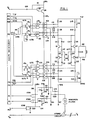
- the total circuit is illustrated in Figure 1 and provides an interface circuit between the telephone lines connected at the TIP and RING terminals and a telephone exchange which communicates control and signalling information with the interface circuit through the computer port.
- the subscriber signals are extracted from the telephone lines by the interface circuit and appear at Ve and Vm where Ve is the signal for transmission along the lines to the earpiece of the user telephone indicated at T and Vm is the signal received from the mouthpiece of the user telephone.
- Ve is the signal for transmission along the lines to the earpiece of the user telephone indicated at T and Vm is the signal received from the mouthpiece of the user telephone.
- These signals can be in analogue form or can, in some circumstances, be in digital form or can be converted to digital form within the exchange.
- the circuit as shown is designed for operation by the user port of a Commodore VIC 20 personal microcomputer and modifications to the circuit to make it compatible with an exchange interface computer will be apparent to one skilled in the art.
- the circuit basically comprises four separate charge pump circuits two associated with the TI P lead and two associated with the RING lead.
- a voltage is applied between the TIP lead and ground by using the charge pumps to charge the capacitor C21 to positive and negative values.
- a voltage is applied to the RING lead relative to ground by charging a capacitor C22.
- a terminal P2 of the computer port controls the charging of the TIP lead to a positive voltage indicated by TP and terminal P4 supplies an enabling signal to charge the TIP lead to a negative voltage as indicated by TN.
- terminals P3 and P5 supply enabling signals charging the RING lead to negative and positive voltages respectively.
- the charging of the capacitors is driven by a square wave signal and supplied by an oscillator terminal PB7.
- the square wave is supplied continuously and generally at a constant frequency but this frequency may lie in the range 250 KHz down to 1 KHz.
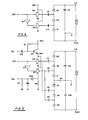
- a single charge pump circuit comprising capacitors C5 and C3 diodes D5, D3 and D1 and part of the integrated circuits IC5 and IC3.
- the square wave signal is supplied to the amplifier of IC5 and is also inverted by the circuit IC7 so as to be supplied in inverted form to the amplifier of IC3.
- the amplifiers IC5, IC3 act as drivers or inverter/ buffers with the output thereof following the square wave, but with one 180° out of phase with the other. The outputs are applied respectively to the capacitors C5 and C3.
- the capacitors have now been charged.
- the power voltage supplied to the amplifiers IC5, IC3 is at a nominal 24 volts therefore making a total voltage drop across the capacitors of 24 volts.
- the output from IC5 then switches from low to high and the output from IC3 switches from high to low when high is 24 volts and low is 0 volts. Since the voltage across C5 and C3 cannot change instantaneously, the other terminals of C5 and C3 follow the change in driver outputs. As the voltage difference across D3 changes to reverse bias, the charges stored in C5 and C3 flow through the circuit including diodes D5 and Dl and charge capacitor C21.
- the process then continually repeats itself so the capacitor C21 is continually charged at 48 volts with current being supplied from the capacitors C5 and C3 only as capacitor C21 is discharged by current flowing in the TIP lead to the remote telephone T.
- Figure 3 in addition to the single charge pump shown in Figure 2, includes a second charge pump provided by the capacitors C4 and C6 and diodes D2, D4 and D6 which in a symmetrical manner to the first charge pump, acts to charge the capacitor C22 to provide a negative voltage at the RING terminal.
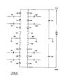
- FIG. 4 is yet further modified to show the four symmetrically arranged charge pumps.
- a further charge pump provided by capacitors C15, C13 and diodes D15, D13, Dll is provided and oriented so as, when enabled, to charge the capacitor C21 to a negative voltage of 48 volts.
- a charge pump provided by capacitors C14, C16 and diodes D12, D14, D16 can, when volts and low is 0 volts. Since the voltage across C5 and C3 cannot change instantaneously, the other terminals of C5 and C3 follow the change in driver outputs. As the voltage difference across D3 changes to reverse bias, the charges stored in C5 and C3 flow through the circuit including diodes D5 and Dl and charge capacitor C21.
- the process then continually repeats itself so the capacitor C21 is continually charged at 48 volts with current being supplied from the capacitors C5 and C3 only as capacitor C21 is discharged by current flowing in the TIP lead to the remote telephone T.
- Figure 3 in addition to the single charge pump shown in Figure 2, includes a second charge pump provided by the capacitors C4 and C6 and diodes D2, D4 and D6 which in a symmetrical manner to the first charge pump, acts to charge the capacitor C22 to provide a negative voltage at the RING terminal.
- FIG. 4 is yet further modified to show the four symmetrically arranged charge pumps.
- a further charge pump provided by capacitors C15, C13 and diodes D15, D13, Dll is provided and oriented so as, when enabled, to charge the capacitor C21 to a negative voltage of 48 volts.
- a charge pump provided by capacitors C14, C16 and diodes D12, D14, D16 can, when enabled, charge the capacitor C22 to a positive voltage.
- the voltage across the TIP and RING terminals can, in accordance with signals provided by the computer port, be controlled to +96V, +48V, -48V and -96V.
- switches Q1 and Q11 are incorporated so that the circuit which is not enable is disconnected in order to prevent discharge of the capacitor directly to ground or to other wire.
- switches Q2 and Q12 are provided for the charge pumps of capacitors C22.
- terminal P6 provides a phasing signal controlling the phase of the oscillating signals applied to IC1 and IC2.
- the phasing signal is indicated at HV.
- the square wave signal indicated at OSC is supplied from the terminal PB7 and enters the quad exclusive or circuit IC7.
- the exclusive or gate IC7a is connected to the signal HV after inversion by an inverter IC9a.
- the gate IC7d is connected directly to the enabling signal HV.
- IC7b is connected to a voltage supply of 5 volts and IC7c is connected to ground with the other terminals of each of the gates being connected to the square wave signal OSC.
- the output pins 3, 11, 4, 10 will carry the signals OSC OSC, OSC and OSC respectively. These signals then enter the quad NAND circuits IC1 and IC2 which steer the oscillating signals to the charge pumps.
- the signals OSC and OSC only appear at the output terminals of ICla and IClc so as to drive the capacitors C5 and C3 through the amplifiers IC5a and IC3a.
- the first charge pump described above is enabled to charge the capacitor C21 to +48 volts thus applying a positive voltage at the TIP lead with the RING lead remaining at ground potential.
- the switches Ql, Q2, Q11, Q12 are provided by transistors as shown.
- the base of the transistor Ql is connected to the base of transistor Q2 through diodes D7, D8 and thence to the capacitor C4 through capacitor C2.
- the base of the transistor Ql is connected to the capacitor C3 through a further capacitor C1.
- the base of the transistor Qll is connected to the transistor Q12 via diodes D17, D18 and thence to the capacitor C14 through a further capacitor C12.
- the base of the transistor Q11 is connected to the capacitor C13 via a further capacitor Cll.
- the signals OSC and OSC drive capacitors C4 and C6 forming a second charge pump including D2, D4 and D6.
- Capacitor C22 is therefore charged making the RING wire negative with respect to ground.
- Transistor Q12 is turned off which prevents discharge of capacitor C22 through diodes D12, D14, D16.
- Transistors Q1 and Q2 in this condition are turned on during each half cycle when driver output supplying capacitor C4 is at high potential and driver output supplying capacitor C3 is at low potential.
- the transistion leading to this state causes current flow through capacitor C2, the base-emitter of Q2, the emitter-base of Q1 and finally capacitor C1. This current turns on both transistors.
- the capacitors Cl and C2 are re-charged through diodes D7 and D8 during the opposite half cycle while transistors Ql and Q2 remain off but do not interfere with the operation of the charge pumps.
- the IC7 output pins 3, 11, 4 and 10 carry the signals OSC, OSC, OSC and OSC.
- Each charge pump will develop only 24 volts and the maximum voltage between the TIP and RING terminals is therefore 48 volts.
- the transmitted signal Ve is supplied at the terminal Ve shown in Figure 1 and also shown in a simplified form in Figure 3.
- This terminal supplies the modulated analogue signal for transmission to the earpiece of the remote telephone.
- the signal is transmitted through a capacitor C19 to the base of a transistor Q3.
- the emitter of the transistor Q3 is connected to the base of a transistor Q4 with collectors of both transistors connected to a positive voltage which is 2 volts above the nominal voltage supplied to the amplifiers IC5, IC3 and also the symmetrical amplifiers IC4 and IC6.
- the transistors Q3 and Q4 introduce a 2-volt potential drop between the 26 volt battery supply and the nominal potential supplied to the amplifiers.
- modulation of the frequency of the square wave can be utilized to provide some control of the rate that the charge pump supplies charge to capacitor C21.
- This effect is achieved due to the fact that capacitors C3 and C5 are often relatively small compared to capacitor C21 and the charge going to capacitor C21 during one wavelength of the square wave will be limited due to a relatively small capacitance of capacitors C3 and C5. If the frequency of the square wave is reduced, capacitors C3 and C5 will discharge less often into capacitor C21 and thus the flow of charge available to capacitor C21 will be decreased and the charge on capacitor C21 will not be as readily changed.
- the frequency of the square wave is increased, the charge on capacitor C21 will be more readily changed. Modulation of the frequency of the square wave is particularly useful in conjunction with switching on and off charge pumps for providing a relatively smooth sinesolidal ringing signal voltage on the telephone lines.
- This 2-volt drop is varied or modulated in accordance with the signal supplied at the terminal Ve. This modulates the amplitude of the 24-volt square waves and therefore varies the voltage generated between TIP and RING terminals for communication to the telephone earpiece of the remote telephone T.
- the current drawn from the capacitors C5 and C15 is measured by measuring the current drawn by the capacitors C5 and C15, which charge the capacitor C21, and by the Capacitors C6 and C16, which charge the capacitor C22.
- the current drawn from these capacitors is determined by measuring the current drawn from the power source by the integrated circuit IC5 and separately by the integrated circuit IC6.
- the current drawn by the circuit IC5 is proportional to the charge required to re-charge the capacitor C21 and symmetrically the current drawn by the circuit IC6 is proportional to the charge required to re-charge the capacitor C22.
- the amplifiers IC5a and IC5b which are associated with separate charge pumps are combined into a single circuit thus enabling a simpler measurement of the total charge drawn by the capacitor C21.
- the current drawn by IC5 is sensed across a resistor R4. Firstly, the peaks of the current are detected using a peak detecting circuit comprising diode D10, resistor R10 and capacitor C10 which is applied to a comparator IC8b. At the same time, the sensed current is passed through a diode D20 and produces a modulated voltage across resistor 7.
- the current drawn by IC6 is sensed across a resistor R3 and communicated firstly to a peak detector comprising diode D9, resistor R9 and capacitor C9 and supplied to a comparator IC8a and secondly, is applied across the resistor R7 by a diode D19.
- the average voltage applied across the resistor R7 through the diodes D19 and D20 is proportional to the current passing through the TIP and RING leads and therefore any modulation thereof is proportional to the signals communicated on the telephone lines.
- This signal is applied to a band pass filter and amplifier having a filter range of 300 Hz to 3,400 Hz to extract analogue voice signals.
- This extracted signal is proportional to a combination of the transmitted Ve signal and also the received Vm signal.
- the Vm signal is extracted from the total by a hybrid circuit of conventional form which receives from the terminal Ve, the transmitted signal and subtracts it from the combined signal to leave Vm which is communicated to the terminal for transmission through the exchange to the remote connection.
- the outputs from the peak detecting circuits as applied to the comparators IC8a and C8b are converted into digital form by a conventional ramp analogue to digital converter technique.
- a ramp circuit receives an input from the terminal PA7 causes the ramp circuit to provide a linearly increasing voltage commencing at 0 volts which voltage is developed at terminal TR1.
- the ramp voltage is applied to the other terminals of the comparators IC8a, IC8b.
- the comparator circuits IC8a, IC8b change stte.
- the time from the initial signal from the terminal PA7 to the change of state of the comparators is measured by the computer attached to the terminals Pl, PO and PA7 whereby digital pulse width signals indicative of the peak current drawn from the TIP and RING lead respectively are supplied to the terminals PO and Pl.
- digital pulse width signals can be used to detect off hook and dial pulse signals on the line. It can also be used to sense leakage current between the TIP wire and RING wire or between the TIP wire and ground and between the RING wire and ground for line test purposes.
- the interface circuit described above therefore enables power voltages and signal voltages to be developed across the TIP and RING terminals and these voltages can be used for controlling the remote telephone equipment and for transmitting the signals to and from the remote telephone equipment.
- the development of voltages is under the control of the microcomputer.
- the circuit is therefore of a very simple nature and is readily compatible with microcomputers currently used in the telephone exchange systems.
Landscapes
- Engineering & Computer Science (AREA)
- Signal Processing (AREA)
- Power Engineering (AREA)
- Devices For Supply Of Signal Current (AREA)
- Interface Circuits In Exchanges (AREA)
Applications Claiming Priority (2)
| Application Number | Priority Date | Filing Date | Title |
|---|---|---|---|
| CA435476 | 1983-08-26 | ||
| CA000435476A CA1197641A (en) | 1983-08-26 | 1983-08-26 | Telephone line interface circuit |
Publications (2)
| Publication Number | Publication Date |
|---|---|
| EP0136077A2 true EP0136077A2 (de) | 1985-04-03 |
| EP0136077A3 EP0136077A3 (de) | 1986-08-27 |
Family
ID=4125954
Family Applications (1)
| Application Number | Title | Priority Date | Filing Date |
|---|---|---|---|
| EP84305784A Withdrawn EP0136077A3 (de) | 1983-08-26 | 1984-08-23 | Fernsprechleitungsschnittstellenschaltung |
Country Status (4)
| Country | Link |
|---|---|
| US (1) | US4578541A (de) |
| EP (1) | EP0136077A3 (de) |
| JP (1) | JPS6070894A (de) |
| CA (1) | CA1197641A (de) |
Cited By (1)
| Publication number | Priority date | Publication date | Assignee | Title |
|---|---|---|---|---|
| EP0237303A1 (de) * | 1986-03-12 | 1987-09-16 | Gpt Limited | Weckschaltung |
Families Citing this family (8)
| Publication number | Priority date | Publication date | Assignee | Title |
|---|---|---|---|---|
| CA1311068C (en) * | 1989-09-29 | 1992-12-01 | Donald Cruickshank | Computer telecommunications signalling interface |
| US5343516A (en) * | 1989-09-29 | 1994-08-30 | Digital Systems Group, Inc. | Computer telecommunications signalling interface |
| US5254877A (en) * | 1992-04-09 | 1993-10-19 | Pittway Corporation | Distributed power supply system |
| EP0707770A4 (de) * | 1993-06-04 | 2005-02-02 | M & Fc Holding Llc | Zählerschnittstelle für einkommenden anruf mit stromversorgung aus der fernsprechleitung |
| EP1017220B1 (de) * | 1998-12-31 | 2007-05-02 | STMicroelectronics S.r.l. | Schaltungsanordnung zur Rufwechselspannungserzeugung für Teilnehmerschaltungen |
| US6873702B1 (en) | 1998-12-31 | 2005-03-29 | Stmicroelectronics S.R.L. | Telephone subscriber system |
| US6940970B2 (en) * | 2001-10-05 | 2005-09-06 | Thomson Licensing S.A. | Ring boost circuit to extend ringing range of telephone SLICs |
| CN103401547B (zh) * | 2013-08-15 | 2016-09-07 | 中国兵器工业集团第二一四研究所苏州研发中心 | 单线双向三电压装定接口电路 |
Family Cites Families (17)
| Publication number | Priority date | Publication date | Assignee | Title |
|---|---|---|---|---|
| US2797261A (en) * | 1954-04-22 | 1957-06-25 | Itt | Carrier telegraph receiver |
| US3849734A (en) * | 1970-09-29 | 1974-11-19 | Grass Instr Co | Signal processing apparatus |
| US3827026A (en) * | 1971-01-04 | 1974-07-30 | Honeywell Inf Systems | Encoding technique for enabling a device to process different types of digital information transmitted along a single information channel |
| GB1424525A (en) * | 1972-05-11 | 1976-02-11 | Elliott Brothers London Ltd | Data transmission system |
| US3904833A (en) * | 1973-06-04 | 1975-09-09 | Superior Continental Corp | Ringing generator circuit with capacitor storage |
| US3875332A (en) * | 1973-12-27 | 1975-04-01 | Nasa | Digital transmitter for data bus communications system |
| US3927266A (en) * | 1974-01-16 | 1975-12-16 | Gte Automatic Electric Lab Inc | Ringer power generator circuit for subscriber carrier station terminal |
| DE2417054C3 (de) * | 1974-04-08 | 1983-02-10 | Siemens AG, 1000 Berlin und 8000 München | Schaltungsanordnung mit zwei miteinander verknüpften Schaltkreissystemen |
| US4001515A (en) * | 1974-11-21 | 1977-01-04 | Astreon Corporation | Interfacing unit for telephone networks |
| US4227053A (en) * | 1978-02-21 | 1980-10-07 | Sava Jacobson | Telephone answering device having balanced input |
| JPS54144113A (en) * | 1978-05-02 | 1979-11-10 | Nitsuko Ltd | Data transmitter*receiver system |
| FR2443770A1 (fr) * | 1978-12-04 | 1980-07-04 | Materiel Telephonique | Recepteur pour bus ac a isolation galvanique par capacite |
| FR2466923A1 (fr) * | 1979-10-05 | 1981-04-10 | Materiel Telephoniqu Thomson C | Circuit de generation et d'injection de sonnerie |
| CA1153076A (en) * | 1979-12-10 | 1983-08-30 | General Electric Company | Resonator coupled differential amplifier |
| US4354062A (en) * | 1980-01-31 | 1982-10-12 | Bell Telephone Laboratories, Incorporated | Communication system signaling circuit |
| US4349703A (en) * | 1980-03-31 | 1982-09-14 | International Telephone And Telegraph Corporation | Programmable ring signal generator |
| US4431868A (en) * | 1981-07-09 | 1984-02-14 | International Telephone And Telegraph Corporation | Solid state telephone line interface circuit with ringing capability |
-
1983
- 1983-08-26 CA CA000435476A patent/CA1197641A/en not_active Expired
- 1983-10-24 US US06/544,952 patent/US4578541A/en not_active Expired - Fee Related
-
1984
- 1984-08-23 EP EP84305784A patent/EP0136077A3/de not_active Withdrawn
- 1984-08-27 JP JP59178175A patent/JPS6070894A/ja active Pending
Cited By (2)
| Publication number | Priority date | Publication date | Assignee | Title |
|---|---|---|---|---|
| EP0237303A1 (de) * | 1986-03-12 | 1987-09-16 | Gpt Limited | Weckschaltung |
| US4737989A (en) * | 1986-03-12 | 1988-04-12 | The General Electric Company, P.L.C. | Ringing circuit |
Also Published As
| Publication number | Publication date |
|---|---|
| JPS6070894A (ja) | 1985-04-22 |
| CA1197641A (en) | 1985-12-03 |
| US4578541A (en) | 1986-03-25 |
| EP0136077A3 (de) | 1986-08-27 |
Similar Documents
| Publication | Publication Date | Title |
|---|---|---|
| EP0136077A2 (de) | Fernsprechleitungsschnittstellenschaltung | |
| CA1202742A (en) | Loop-start/ground-start line interface circuit | |
| EP0178993B1 (de) | Eingangsschaltungsstruktur für eine Teilnehmerleitungsschnittstelle | |
| US5708701A (en) | Power line telephone communications system having on hook digital voiceband messaging | |
| US4860346A (en) | Telephone system and method operated from central office loop current | |
| GB1185678A (en) | A Telephone System | |
| NZ238697A (en) | Line interface circuit | |
| JPS61288696A (ja) | 電話線表示回路 | |
| EP0729259B1 (de) | Rufsignalerzeugung in einer Teilnehmerschaltung (SLIC) | |
| US4860345A (en) | Telephone system and method operated from central office loop current | |
| US4617426A (en) | Method for current supply to a subscriber telephone from a telephone exchange | |
| CN1258159A (zh) | 用于辅助设备的由电话线供电的电源及其操作方法 | |
| EP0143435B1 (de) | Monolithisch integrierte Fernsprechschaltungen für Rufabschaltungserkennung | |
| US4720852A (en) | Monolithically integratable telephone circuit for generating control signals for displaying the telephone charges to a subscriber | |
| JPS58151160A (ja) | 呼出信号送出方式 | |
| US4674118A (en) | Telephone line hold and hold release apparatus | |
| JP3473125B2 (ja) | 端末網制御装置 | |
| GB2126045A (en) | Subscriber carrier system | |
| JP3048368B2 (ja) | 端末器用電源回路 | |
| US4127747A (en) | Voltage boost circuit for telephone systems | |
| US6411694B1 (en) | Arrangement for improving a telephone system | |
| JP2950092B2 (ja) | 極性反転検出回路及びこの回路を用いた端末装置 | |
| JPH08163281A (ja) | 電話回線を利用した自動管理システムにおける電源装置 | |
| JP3057930B2 (ja) | 端末網制御装置 | |
| JPS6325791Y2 (de) |
Legal Events
| Date | Code | Title | Description |
|---|---|---|---|
| PUAI | Public reference made under article 153(3) epc to a published international application that has entered the european phase |
Free format text: ORIGINAL CODE: 0009012 |
|
| AK | Designated contracting states |
Designated state(s): AT BE CH DE FR GB IT LI LU NL SE |
|
| PUAL | Search report despatched |
Free format text: ORIGINAL CODE: 0009013 |
|
| AK | Designated contracting states |
Kind code of ref document: A3 Designated state(s): AT BE CH DE FR GB IT LI LU NL SE |
|
| 17P | Request for examination filed |
Effective date: 19870227 |
|
| 17Q | First examination report despatched |
Effective date: 19890315 |
|
| 18D | Application deemed to be withdrawn |
Effective date: 19920422 |
|
| RIN1 | Information on inventor provided before grant (corrected) |
Inventor name: DODDS, DAVID E. |