EP0135359B1 - Schaltbarer Fiberoptischer Koppler - Google Patents
Schaltbarer Fiberoptischer Koppler Download PDFInfo
- Publication number
- EP0135359B1 EP0135359B1 EP84305496A EP84305496A EP0135359B1 EP 0135359 B1 EP0135359 B1 EP 0135359B1 EP 84305496 A EP84305496 A EP 84305496A EP 84305496 A EP84305496 A EP 84305496A EP 0135359 B1 EP0135359 B1 EP 0135359B1
- Authority
- EP
- European Patent Office
- Prior art keywords
- coupler
- optical
- light
- phase shift
- fibers
- Prior art date
- Legal status (The legal status is an assumption and is not a legal conclusion. Google has not performed a legal analysis and makes no representation as to the accuracy of the status listed.)
- Expired - Lifetime
Links
- 239000000835 fiber Substances 0.000 title description 99
- 239000013307 optical fiber Substances 0.000 claims abstract description 61
- 230000003287 optical effect Effects 0.000 claims abstract description 45
- 230000010363 phase shift Effects 0.000 claims description 29
- 239000013078 crystal Substances 0.000 claims description 26
- 230000008878 coupling Effects 0.000 claims description 23
- 238000010168 coupling process Methods 0.000 claims description 23
- 238000005859 coupling reaction Methods 0.000 claims description 23
- 230000001066 destructive effect Effects 0.000 claims description 5
- 238000000034 method Methods 0.000 claims description 2
- 230000003993 interaction Effects 0.000 description 17
- 239000000463 material Substances 0.000 description 11
- 230000010287 polarization Effects 0.000 description 9
- 239000000382 optic material Substances 0.000 description 7
- 238000005253 cladding Methods 0.000 description 5
- VYPSYNLAJGMNEJ-UHFFFAOYSA-N Silicium dioxide Chemical compound O=[Si]=O VYPSYNLAJGMNEJ-UHFFFAOYSA-N 0.000 description 3
- 230000008901 benefit Effects 0.000 description 3
- 239000002131 composite material Substances 0.000 description 3
- 238000005286 illumination Methods 0.000 description 3
- 238000004519 manufacturing process Methods 0.000 description 3
- 238000012544 monitoring process Methods 0.000 description 3
- 238000000926 separation method Methods 0.000 description 3
- 230000003111 delayed effect Effects 0.000 description 2
- 230000001419 dependent effect Effects 0.000 description 2
- 239000005350 fused silica glass Substances 0.000 description 2
- 239000003921 oil Substances 0.000 description 2
- 239000000126 substance Substances 0.000 description 2
- 230000009471 action Effects 0.000 description 1
- 239000000654 additive Substances 0.000 description 1
- 230000000996 additive effect Effects 0.000 description 1
- 239000004568 cement Substances 0.000 description 1
- 238000010276 construction Methods 0.000 description 1
- 230000001808 coupling effect Effects 0.000 description 1
- 238000010586 diagram Methods 0.000 description 1
- 230000000694 effects Effects 0.000 description 1
- 229920006335 epoxy glue Polymers 0.000 description 1
- 230000006870 function Effects 0.000 description 1
- 239000011521 glass Substances 0.000 description 1
- 239000003365 glass fiber Substances 0.000 description 1
- 238000010438 heat treatment Methods 0.000 description 1
- 230000001939 inductive effect Effects 0.000 description 1
- 238000010587 phase diagram Methods 0.000 description 1
- 238000005498 polishing Methods 0.000 description 1
- 230000001902 propagating effect Effects 0.000 description 1
- 230000004044 response Effects 0.000 description 1
- 230000009131 signaling function Effects 0.000 description 1
- 229910052710 silicon Inorganic materials 0.000 description 1
- 239000010703 silicon Substances 0.000 description 1
- 239000007787 solid Substances 0.000 description 1
Images
Classifications
-
- G—PHYSICS
- G02—OPTICS
- G02B—OPTICAL ELEMENTS, SYSTEMS OR APPARATUS
- G02B6/00—Light guides; Structural details of arrangements comprising light guides and other optical elements, e.g. couplings
- G02B6/24—Coupling light guides
-
- G—PHYSICS
- G02—OPTICS
- G02B—OPTICAL ELEMENTS, SYSTEMS OR APPARATUS
- G02B6/00—Light guides; Structural details of arrangements comprising light guides and other optical elements, e.g. couplings
- G02B6/24—Coupling light guides
- G02B6/26—Optical coupling means
- G02B6/35—Optical coupling means having switching means
- G02B6/3502—Optical coupling means having switching means involving direct waveguide displacement, e.g. cantilever type waveguide displacement involving waveguide bending, or displacing an interposed waveguide between stationary waveguides
-
- G—PHYSICS
- G02—OPTICS
- G02B—OPTICAL ELEMENTS, SYSTEMS OR APPARATUS
- G02B6/00—Light guides; Structural details of arrangements comprising light guides and other optical elements, e.g. couplings
- G02B6/24—Coupling light guides
- G02B6/26—Optical coupling means
- G02B6/28—Optical coupling means having data bus means, i.e. plural waveguides interconnected and providing an inherently bidirectional system by mixing and splitting signals
- G02B6/2804—Optical coupling means having data bus means, i.e. plural waveguides interconnected and providing an inherently bidirectional system by mixing and splitting signals forming multipart couplers without wavelength selective elements, e.g. "T" couplers, star couplers
- G02B6/2821—Optical coupling means having data bus means, i.e. plural waveguides interconnected and providing an inherently bidirectional system by mixing and splitting signals forming multipart couplers without wavelength selective elements, e.g. "T" couplers, star couplers using lateral coupling between contiguous fibres to split or combine optical signals
-
- G—PHYSICS
- G02—OPTICS
- G02B—OPTICAL ELEMENTS, SYSTEMS OR APPARATUS
- G02B6/00—Light guides; Structural details of arrangements comprising light guides and other optical elements, e.g. couplings
- G02B6/24—Coupling light guides
- G02B6/26—Optical coupling means
- G02B6/28—Optical coupling means having data bus means, i.e. plural waveguides interconnected and providing an inherently bidirectional system by mixing and splitting signals
- G02B6/2804—Optical coupling means having data bus means, i.e. plural waveguides interconnected and providing an inherently bidirectional system by mixing and splitting signals forming multipart couplers without wavelength selective elements, e.g. "T" couplers, star couplers
- G02B6/2861—Optical coupling means having data bus means, i.e. plural waveguides interconnected and providing an inherently bidirectional system by mixing and splitting signals forming multipart couplers without wavelength selective elements, e.g. "T" couplers, star couplers using fibre optic delay lines and optical elements associated with them, e.g. for use in signal processing, e.g. filtering
-
- G—PHYSICS
- G02—OPTICS
- G02B—OPTICAL ELEMENTS, SYSTEMS OR APPARATUS
- G02B6/00—Light guides; Structural details of arrangements comprising light guides and other optical elements, e.g. couplings
- G02B6/24—Coupling light guides
- G02B6/26—Optical coupling means
- G02B6/35—Optical coupling means having switching means
- G02B6/3586—Control or adjustment details, e.g. calibrating
- G02B6/3588—Control or adjustment details, e.g. calibrating of the processed beams, i.e. controlling during switching of orientation, alignment, or beam propagation properties such as intensity, size or shape
-
- G—PHYSICS
- G02—OPTICS
- G02B—OPTICAL ELEMENTS, SYSTEMS OR APPARATUS
- G02B6/00—Light guides; Structural details of arrangements comprising light guides and other optical elements, e.g. couplings
- G02B6/24—Coupling light guides
- G02B6/26—Optical coupling means
- G02B6/35—Optical coupling means having switching means
- G02B6/354—Switching arrangements, i.e. number of input/output ports and interconnection types
- G02B6/3544—2D constellations, i.e. with switching elements and switched beams located in a plane
- G02B6/3546—NxM switch, i.e. a regular array of switches elements of matrix type constellation
-
- G—PHYSICS
- G02—OPTICS
- G02B—OPTICAL ELEMENTS, SYSTEMS OR APPARATUS
- G02B6/00—Light guides; Structural details of arrangements comprising light guides and other optical elements, e.g. couplings
- G02B6/24—Coupling light guides
- G02B6/26—Optical coupling means
- G02B6/35—Optical coupling means having switching means
- G02B6/3564—Mechanical details of the actuation mechanism associated with the moving element or mounting mechanism details
- G02B6/3568—Mechanical details of the actuation mechanism associated with the moving element or mounting mechanism details characterised by the actuating force
- G02B6/3578—Piezoelectric force
-
- G—PHYSICS
- G02—OPTICS
- G02B—OPTICAL ELEMENTS, SYSTEMS OR APPARATUS
- G02B6/00—Light guides; Structural details of arrangements comprising light guides and other optical elements, e.g. couplings
- G02B6/24—Coupling light guides
- G02B6/26—Optical coupling means
- G02B6/35—Optical coupling means having switching means
- G02B6/3594—Characterised by additional functional means, e.g. means for variably attenuating or branching or means for switching differently polarized beams
Definitions
- This invention relates to active devices for multiplexing or switching optical signals in fiber optic systems, and specifically to a switchable coupler which selectively couples light from an input optical fiber to either of two output optical fibers.
- Fiber optic multiplexing or switching in the past has been accomplished using passive frequency selective couplers, such as that described in Patent No. US-A-3,957,341, in which a pair of coupled waveguides have different phase propagation constants at all frequencies except for the frequency to be coupled, yielding a separation of this frequency from all other frequencies.
- passive frequency selective couplers such as that described in Patent No. US-A-3,957,341, in which a pair of coupled waveguides have different phase propagation constants at all frequencies except for the frequency to be coupled, yielding a separation of this frequency from all other frequencies.
- Such systems require careful material selection for the desired frequency separation and do not lend themselves to adjustment during or after manufacture to accomplish the separation of optical signals over a broad range of frequencies.
- fiber optic multiplexing has been accomplished using active systems in which a pair of waveguides are surrounded by a crystal material which has a voltage responsive refractive index. Such systems are difficult to manufacture and typically have a fairly narrow bandwidth of operation.
- the invention described herein is defined in claim 1; in particular it comprises an optical switch having first and second optical couplers, each comprising first and second optical fibers which are relatively positioned to provide partial light coupling therebetween.
- the first and second optical fibers of the first coupler are optically connected, respectively, to the first and second optical fibers of the second coupler.
- the optical switch includes means, interposed between the first optical fiber of the first coupler and the first optical fiber of the second coupler, for introducing a variable phase shift to light transmitted therebetween. This variable phase shift causes light to selectively interfere within the second coupler, so that the second coupler selectively supplies a major portion of light which was input to the first optical fiber of the first coupler, alternatively, to the first or second optical fiber of the second optical coupler.
- the optical switch additionally includes means for adjusting the variable phase shift in accordance with the wavelength of light supplied to the optical switch.
- means are provided for sensing a level of light output from said second optical coupler, and for providing a feedback signal to the means for adjusting the variable phase shift.
- the means for providing a feedback signal functions to cause a light output at only one of either of said first and second optical fibres of said second optical coupler.
- the invention also comprises a method as defined in claim 7
- the present invention provides a fiber optic switching coupler system in which single mode optical fiber couplers are utilized to selectively couple a light input signal from a single input fiber to either of a pair of output fibers or, in the alternative, to selectively couple signals from either of a pair of input fibers to a single output optical fiber.
- the switching system is based upon single mode optical fiber couplers in which a pair of single mode fibers are positioned adjacent to one another through a selectable interaction length to permit evanescent field coupling.
- the fibers are mounted in a pair of bases or blocks having respective arcuate grooves for mounting the respective strands of fiber optic material.
- material is removed by simultaneously polishing the blocks and the strands until the desired amount of fiber optic material has been removed. The blocks are then positioned in a face-to-face relationship with the strands positioned in close proximity to each other, and with the cutaway portions of the fiber in facing relationship.
- the amount of material removed from the fibers be carefully controlled so that the spacing between the core portions of the fibers is within a predetermined "critical zone". This causes each strand to receive a significant portion of the evanescent filed energy from the other strand, and coupling is achieved without significant energy loss.
- the coupler used in the switching assembly of the present invention may be adjusted so that the coupled power may be changed.
- the couplers used in the present invention are preferably adjusted so that they couple 50% of the light entering each fiber to the other fiber in the fiber pair.
- this coupler adjustment is accomplished by translating the fibers so that their respective facing surfaces are slidingly offset relative to one another.
- an important feature of the coupler which is preferably used in this invention is its capability of achieving low throughput losses.
- Experimental results show that throughput losses of 0.2 db have been attained, although losses of 0.5 db are more common.
- the above-described coupler preferably has a high directivity with substantially all of the coupled power being delivered to the output side of the coupler. Tests have shown that the directionally coupled power is greater than 60 db above the contradirectionally coupled power.
- a pair of couplers is preferably utilized.
- one of the optical fiber strands of the first coupler is used as an input for the switch. Since the couplers are preferably adjusted to have a coupling efficiency of 50%, half of the input light is output on each of the optical fiber strands at the output side of this first coupler.
- An important characteristic of the coupler used in this preferred embodiment is the fact that the coupled light lags in phase by 90 with respect to the uncoupled light at the output side of the coupler, assuming that the fiber optic strands each have the same length.
- the light coupled from one fiber to the other is phase shifted.
- a 90° phase relationship exists between the light outputs.
- One of the fibers from the output side of the first coupler in this preferred embodiment may be coupled directly to one of the fibers at the input of the second coupler.
- throughput losses for the switching device are minimized in this embodiment if only two fibers are used in the device, such that a single fiber forms one of the optical fiber pairs for both couplers.
- the second optical fiber at the output side of the first coupler is preferably arranged to have a variable length before entering the input side of the second coupler.
- this output fiber may be wound around a piezoelectric crystal before entering the input side of the second coupler.
- the piezoelectric crystal is an electro-mechanical transducer which changes in diameter in response to an applied electrical signal.
- the pair of optical fibers entering the input side of the second coupler may each have a length equal to an even number of wavelengths of the light being switched.
- coupled light is preferably phase shifted with respect to uncoupled light by 90°, as explained previously.
- the illumination initially supplied to one of the optical fibers at the input side of the first copier may be selectively output at either of the optical fibers at the output side of the second coupler. This occurs as a consequence of constructive or destructive interference of the lightwaves in the output optical fibers.
- the output illumination on each of the optical fibers at the output side of the second coupler preferably includes a contribution from each fiber at the input side of the second coupler, the contribution from one input fiber being coupled and the contribution from the other input fiber being uncoupled. If the phase relationship between these two contributions is constructive, the output will provide a virtually unattenuated light signal. If, however, the contributions destructively interfere, the output will provide virtually no light signal.
- the phase relationship between the light signals on the pair of optical fibers at the input side of the second coupler is such that, when the piezoelectric crystal has a first electrical signal, the light signals will constructively add in one fiber at the output side of the second coupler and destructively cancel one another at the alternate output.
- the signal at the piezoelectric transducer is changed to induce the 180° phase shift described above, the phase relationship at the output fibers of the second coupler will reverse, so that the alternate fiber outputs the light signal.
- phase shifts other than 180° at the piezoelectric crystal by inducing phase shifts other than 180° at the piezoelectric crystal, other combinations of output signals may be achieved so that, for example, the pair of output fibers may alternately carry all of the signal or each may carry a selected portion of the light signal.
- the pair of optical fibers between the pair of optical couplers are preferably made the same length, at least within the coherence length of the light signals being supplied to the switch, since this is necessary for constructive or destructive interference at the output coupler.
- polarization control may be advantageously provided in the switch to assure such interference.
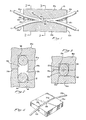
- This coupler 10 is illustrated in Figures 104 and includes two strands 12A and 12B of a single mode fiber optic material mounted in longitudinal arcuate grooves 13A and 13B, respectively, formed in optically flat, confronting surfaces 14A and 14B, respectively, of rectangular bases or blocks 16A and 16B, respectively.
- the block 16A with the strand 12A mounted in the groove 13A will be referred to as the coupler half 10A
- the block 16B with the strand 12B mounted in the groove 13B will be referred to as coupler half 10B.
- Each of the strands 12A and 12B comprise a commercially available fiber of quartz glass which is doped to have a central core and an outer cladding.
- the strands 12A and 12B are single mode fibers, which typically have a core diameter on the order of 10 microns or less and a cladding diameter on the order of 125 microns. In the embodiment disclosed, the diameters of the strands 12 and their respective cores are exaggerated.
- the arcuate grooves 13A and 13B have a radius of curvature which is very large compared to the diameter of the fibers 12, and have a width slightly larger than the fiber diameter to permit the fibers 12, when mounted therein, to conform to a path defined by the bottom walls of the grooves 13.
- the depth of the grooves 13A and 13B varies from a minimum at the center of the blocks 16A and 16B, respectively, to a maximum at the edges of the blocks 16A and 16B, respectively.
- the grooves 13 are illustrated as being rectangular in cross-section, however, it will be understood that other suitable cross-sectional contours which will accommodate the fibers 12 may be used alternatively, such as a U-shaped cross-section or a V-shaped cross-section.
- the depth of the grooves 13 which mount the strands 12 is less than the diameter of the stands 12, while at the edges of the blocks 26, the depth of the grooves 13 is preferably at least as great as the diameter of the strands 12.
- Fiber optic material was removed from each of the strands 12A and 12B to form the respective oval-shaped planar surfaces 18A, 18B, which are coplanar with the confronting surfaces 14A, 14B, respectively. These surfaces 18A, 18B will be referred to herein as the fiber "facing surfaces".
- the amount of fiber optic material removed increases gradually from zero towards the edges of the block 16 to a maximum towards the center of the block 16. This tapered removal of the fiber optic material enables the fibers to converge and diverge gradually, which is advantageous for avoiding backward reflection and excess loss of light energy.
- the coupler halves 10A and 10B are identical, and are assembled by placing the confronting surfaces 14A and 14B of the blocks 16A and 16B together, so that the facing surfaces 18A and 18B of the strands 12A and 12B are in facing relationship.
- index matching substance such as index matching oil, is provided between the confronting surfaces 14.
- This substance has a refractive index approximately equal to the refractive index of the cladding, and also functions to prevent the optically flat surfaces 14 from becoming permanently locked together.
- the oil is introduced between the blocks 16 by capillary action.
- An interaction region 32 is formed at the junction of the strands 12, in which light is transferred between the strands by evanescent field coupling. It has been found that, to insure proper evanescent field coupling, the amount of material removed from the fibers 12 must be carefully controlled so that the spacing between the core portions of the strands 12 is within a predetermined "critical zone".
- the evanescent fields extend into the cladding and decrease rapidly with distance outside their respective cores. Thus, sufficient material should be removed to permit each core to be positioned substantially within the evanescent field of the other. If too little material is removed, the cores will not be sufficiently close to permit the evanescent fields to cause the desired interaction of the guided modes, and thus, insufficient coupling will result.
- each strand receives a significant portion of the evanescent field energy from the other strand, and good coupling is achieved without significant energy losses.
- the critical zone is illustrated schematically in Figure 5 as including that area, designated by the reference numeral 33, in which the evanescent fields, designated by reference numerals 34A and 34B, of the fibers 12A and 12B, respectively, overlap with sufficient strength to provide coupling, i.e., each core is within the evanescent field of the other.
- mode perturbation occurs within the area 33 when the cores are brought too close together.
- the critical zone is defined as that area in which the evanescent fields 34 overlap with sufficient strength to cause coupling without substantial mode perturbation induced power loss.
- the critical zone for a particular coupler is dependent upon a number of interrelated factors such as the parameters of the fiber itself and the geometry of the coupler. Further, for a single mode fiber having a step-index profile, the critical zone can be quite narrow. In a single mode fiber coupler of the type shown in figures 1-4, for example, the required center-to-center spacing between the strands 12 at the center of the coupler is typically less than a few (e.g., 2-3) core diameters.
- the strands 12A and 12B are (1) identical to each other, (2) have the same radius of curvature at the interaction region 32, and (3) have an equal amount of fiber optic material removed therefrom to form their respective racing surfaces 18A and 18B.
- the fibers 12 are symmetrical, through the interaction region 32, in the plane of the facing surfaces 18, so that the facing surfaces 18 are coextensive if superimposed. This insures that the two fibers 12A and 12B will have the same propagation characteristics at the interaction region 32, and thereby avoids coupling attenuation associated with dissimilar propagation characteristics.
- the blocks or bases 12 may be fabricated of any suitable rigid material.
- the bases 12 comprise generally rectangular blocks of fused quartz glass approximately 1 inch long, 1 inch wide, and 0.4 inch thick.
- the fiber optic strands 12 are secured in the slots 13 by suitable cement 38, such as epoxy glue.
- suitable cement 38 such as epoxy glue.
- One advantage of the fused quartz blocks 16 is that they have a coefficient of thermal expansion similar to that of glass fibers, and this advantage is particularly important if the blocks 16 and fibers 12 are subjected to any heat treatment during the manufacturing process.
- Another suitable material for the block 16 is silicon, which also has excellent thermal properties for this application.
- the coupler 10 includes four ports, labeled A, B, C, and D in Figure 1.
- ports A and C which correspond to strands 12A and 12B, respectively, are on the left-hand side of the coupler 10
- the ports B and D which correspond to the strands 12A and 12B, respectively, are on the right-hand side of the coupler 10.
- input light is applied to port A.
- This light passes through the coupler and is output at port B and/or port D, depending upon the amount of power that is coupled between the strands 12.
- the term "normalized coupled power" is defined as the ratio of the coupled power to the total output power.
- the normalized coupled power would be equal to the ratio of the power at port D to the sum of the power output at ports B and D. This ratio is also referred to as the "coupling efficiency", and when so used is typically expressed as a percent.
- the corresponding coupling efficiency is equal to the normalized coupled power times 100.
- tests have shown that the coupler 10 has a coupling efficiency of up to 100%.
- the coupler 10 may be "tuned” to adjust the coupling efficiency to any desired value between zero and the maximum.
- the coupler 10 is highly directional, with substantially all of the power applied at one side of the coupler being delivered to the other side of the coupler.
- the coupler directivity is defined as the ratio of the power at port D to the power at port c, with the input applied to port A. Tests have shown that the directionally coupled power (at port D) is greater than 60 db above the contra-directionally coupled power (at port C).
- the coupler directivity is symmetrical. That is, the coupler operates with the same characteristics regardless of which side of the coupler is the input side and which side is the output side. Moreover, the coupler 10 achieves these results with very low throughput losses.
- the throughput loss is defined as the ratio of the total output power (ports B and D) to the input power (port A) subtracted from one (i.e., 1 - (P B + P D )/P A ).
- Experimental results show that throughput losses of 0.2 db have been obtained, although losses of 0.5 db are more common. Moreover, these tests indicate that the coupler 10 operates substantially independently of the polarization of the input light applied.
- the coupler 10 operates on evanescent field coupling principles in which guided modes of the strands 12interact, through their evanescent fields, to cause light to be transferred between the strands 12. As previously indicated, this transfer of light occurs at the interaction region 32. The amount of light transferred is dependent upon the proximity and orientation of the cores, as well as the effective length of the interaction region 32.
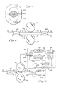
- a pair of optical fiber couplers 42 and 44 constructed in accordance with the description provided above in reference to Figures 1-5, each include a pair of input ports, labeled A and C, and a pair of output ports, labeled B and D.
- an input light signal is supplied to input port A of the coupler 42.
- This input light signal is designated 11.
- each of the couplers 42 and 44 are manufactured and properly adjusted so that their coupling efficiency is 50%. That is, 50% of the light signal 1 1 will remain uncoupled to exit the coupler at port B. This signal is labeled 1 2 .
- the remaining 50% of the input illumination is coupled by the coupler 42 and is output at port D of the coupled 42, designated 1 3 .
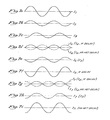
- the input light signal 11 is shown as having a characteristic amplitude and phase.
- Figure 7B shows that the uncoupled portion of the light signal 1 1 , which exits port B of the coupler 42, has the same relative phase as the signal 11, but an amplitude which is 50% of the amplitude of the signal I 1 .
- Figure 7C shows that the light signal 1 3 has an amplitude reduced by 50%, but is shifted in phase relative to the signal 1 1 by 90°. This phase shift occurs as a direct consequence of the coupling in the interaction region of the coupler 42.
- phase shift may be considered to be 90°, as shown in Figures 7A and 7C. It will become apparent, however, through the description of Figure 8, that the system need not have these local characteristics to operate.
- the fiber 12A which exits the coupler 42 at port B and across the light signal 1 2 , is wrapped, at least once, around a cylindrical, radially polarized piezoelectric crystal 46, and continues through ports A and B of the coupler 44.
- the fiber 12B after exiting port D of the coupler 42, is wrapped on a passive cylindrical mandrel 48, identical in shape to the piezoelectric crystal 46, and thereafter passes through ports C and D of the coupler 44.
- the switch assembly includes only the two fibers 12A and 12B in this exemplary embodiment, although it will be understood that, by splicing fibers together, the assembly shown in Figure 6 may be constructed with multiple fiber segments, if the greater loss, which occurs at splices, is tolerable in the overall switching system.
- the relative phase relationship between the signals I 4 and I 5 at the input ports A and C, respectively, of the coupler 44 may be assumed to be identical to the phase relationship of the signals 1 2 and 1 3 , shown respectively in Figures 7B and 7C. That is, the signal I 5 at port C of the coupler 44 lags the signal I 4 at port A of the coupler 44 by 90°.
- the coupler 44 is also manufactured and adjusted to provide a 50% coupling efficiency.
- the light output at port B designated I 6
- the light signal output at port D designated I 7
- the light signal output at port D will include two components: (a) the uncoupled 50% of the light signal I 5 and (b) the coupled 50% of the light signal 1 4 .
- the coupled component will be phase shifted by 90° at the interaction region of the coupler 44.
- Figure 7D shows, in solid lines, the component of the signal I 6 which results from the uncoupled 50% portion of the signal 1 4 , designated I 6 (I4).
- the Figure 7E shows the component of the signal 1 6 which results from the coupled 50% of the light signal I 5 , designated I 6 (1 5 ), which signal is 90° phase shifted from the signal 1 3 of Figure 7C.
- the light signal at port D of the coupler 44, I 7 includes two components.
- the first of these components is the uncoupled portion of the light signal I 5 , shown in Figure 7H as I 7 (1 5 ).
- the other component of the signal I 7 is shown in solid lines in figure 7G as 1 7 -(I4), that is, the coupled 50% of the light signal 1 4 .
- the signals I 7 (1 5 ) and I 7 (I 4 ) are in phase, and thus constructively add to produce, at the output I 7 , the signal shown in Figure 71, namely, the input signal 1 1 shown in Figure 7A, phase shifted by 90°.
- the light signal input at port A of the coupler 42, I 1 is thus output at the port D of the coupler 44, I 7 , with no light output from port B of the computer 44.
- the resulting signal I 6 which appears at port B of the coupler 44, is a composite of I 6 (I 4 ) shown in dashed lines in Figure 7D and I 6 (1 5 ) shown in Figure 7E, that is, a composite of the uncoupled, delayed signal I 4 and the coupled signal I 5 .
- These signals as shown in Figure 7D and 7E, are in phase, and thus will constructively add at port B of the coupler 44, yielding the signal shown in Figure 7F.
- the signal at port D of the coupler 44, I 7 is a composite of the coupled portion of the delayed signal 1 4 , I 7 (I4), shown in dashed lines in Figure 7G, and the uncoupled portion of the signal I 5 , that is, I 7 (1 5 ).
- I 7 the uncoupled portion of the signal I 5 , that is, I 7 (1 5 ).
- the input signal at port A of the coupler 42 will be split between the output ports B and D of the coupler 44.
- a feedback system is shown which may be utilized to provide the voltage signals used for driving the piezoelectric crystal 46 to operate the switch of Figure 6 between its two extreme positions, that is, to provide an output signal alternatively at port B or port D of the coupler 44.
- a pair of sensors 52 and 54 are connected to the optical fibers 12A and 12B adjacent the ports B and D of the coupler 44. These sensors may be, for example, photodiodes which are mounted adjacent a bend in the optical fibers 12A and 12B or may be a photodiode located at a point on the fibers 12A and 12B where the cladding has been polished sufficiently to permit escape, and thus monitoring, of a small portion of the light transmitted by the fibers. The sensors 52 and 54 thus provide a means for monitoring the light level at ports B and D of the coupler 44.
- An input signal on a line 56 is used to control the switchable coupler by controlling a switch 58 which alternatively conducts a voltage signal from a first voltage source 60 or a second voltage source 62 to the piezoelectric crystal 46.
- the voltage source 60 provides a voltage level V 1 sufficient to stretch the optical fiber 12A wrapped around the piezoelectric crystal 46 to introduce a half wavelength net relative delay in the light transmitted by the fiber 12A between port B of the coupler 42 and port A of the coupler 44, so that the light signal 1 1 input at port A of the coupler 42 will constructively add at port B of the coupler 44 but will destructively interfere at port D of the coupler 44 in the manner previously described.
- the voltage source 62 provides a voltage signal V 2 which produces effectively no net relative delay at the piezoelectric crystal 46, so that the light signals 1 4 and 1 5 bear the same relative phase relationship as the light signals 1 2 and 1 3 , shown in Figures 7B and 7C.
- the term "net relative” delay means the effective phase difference between uncoupled light on the fibers 12A and 12B. That is, “no net relative delay” means that the length of the optical fiber 12A between the interaction region of the coupler 42 and the interaction region of the coupler 44 differs from the length of the optical fiber 12B between these interaction regions by an amount NX, where N is an integer (including 0), and X is the wavelength of the light signal I 1 . Similarly, "half wavelength net relative delay” means that the difference in length of the fibers 12A and 12B between the interaction regions of the couplers 42 and 44 is NX + 1/2X, where N an dX are defined as stated above.
- the switch 58 also provides a pair of output control signals on a pair of lines 64 and 66 to operate a pair of slave switches 68 and 70, respectively.
- the switch 58 conducts the voltage signal V 1 from the source 60 to the piezoelectric crystal 46, the switch 68 is closed, while the switch 70 is opened.
- the switch 70 is closed while the switch 68 is opened.
- the switch 70 connects the photosensor 52 to a null servo 72 while the switch 68, when closed, connects to photosensor 54 to a null servo 74.
- the switches 58, 68 and 70 are typically solid state switching devices and the null servos 72 and 74 are prior art devices which provide an output signal on their output lines 76 and 78, respectively, which is a variable DC voltage feedback signal used to adjust the input signal to the servos 72 and 74 to a null condition.
- the switch 58 when the switch 58 conducts the output of the source 60 to the piezoelectric crystal 46, all of the input light signal 1 1 should be coupled to the output 1 6 , since the voltage V 1 is intended to stretch the fiber 12A by one-half wavelength.
- the photosensor 54 through the switch 68, provides at the input to the null servo 74, a signal which represents the light level of the signal 1 7 at port D of the coupler 44, which should be zero.
- the null servo 74 adjusts the output signal 78 and, in turn, the voltage V 1 of the source 60 in a manner necessary to make the light output at port D of the coupler 44 zero.
- the switch 70 permits the null servo 72 to monitor the light output at port B of the coupler 44 by monitoring the output of the photosensor 52. In this position of the switch 58, the null servo 72 will provide an output signal 76 to adjust the voltage source 62 to provide zero output at port B of the coupler 44.
- the switches 68 and 70 assure that each of the servos 72 and 74 will receive an input signal only when the input signal on line 56 to the switchable coupler indicates that a null output should exist at the respective photodetector 54 or 52. In this manner, regardless of the wavelength of the signal 1 1 , the system will automatically adjust the output voltage provided to the piezoelectric crystal 46 to assure switching between ports B and D of the coupler 44. It will be understood that when the switch 70 is non-conductive, the null servo 72 will receive no light output signal and will thus provide a constant output signal on line 76 to maintain the current adjustment of the source 62. Thus, the signals 76 and 78 are only adjusted by the servos 72 and 74, respectively, when a non-null signal is provided by the photodetectors 52 and 54 in the operational mode where these photodetectors should provide a null output.
- the polarization of the waves from the ports B and D at the input of the coupler 44 must be identical. Without this identical polarization, complete additive or destructive interference cannot be accomplished. Therefore, it may be advantageous to include a polarization controller 82 to one of the fibers 12A, 12B to adjust the polarization to match that of the other fiber.
- the polarization controller 82 may be constructed in accordance with the teachings of United States Patent No. 4,389,090, entitled “Fiber Optic Polarization Controller", which is hereby incorporated herein by reference.
- this switchable coupler provides a means for switching an input light signal at port A of the coupler 42 to either of two output optical fibers at ports B and D of the coupler 44.
- the switchable coupler will couple an input light signal on either port B or port D of the coupler 44 to port A of the coupler 42.
Landscapes
- Physics & Mathematics (AREA)
- General Physics & Mathematics (AREA)
- Optics & Photonics (AREA)
- Engineering & Computer Science (AREA)
- Signal Processing (AREA)
- Theoretical Computer Science (AREA)
- Optical Communication System (AREA)
- Mechanical Light Control Or Optical Switches (AREA)
- Keying Circuit Devices (AREA)
- Pens And Brushes (AREA)
- Switches Operated By Changes In Physical Conditions (AREA)
- Light Guides In General And Applications Therefor (AREA)
- Push-Button Switches (AREA)
- Mechanical Coupling Of Light Guides (AREA)
- Coupling Device And Connection With Printed Circuit (AREA)
Claims (7)
Priority Applications (1)
| Application Number | Priority Date | Filing Date | Title |
|---|---|---|---|
| AT84305496T ATE71739T1 (de) | 1983-08-15 | 1984-08-13 | Schaltbarer fiberoptischer koppler. |
Applications Claiming Priority (2)
| Application Number | Priority Date | Filing Date | Title |
|---|---|---|---|
| US06/523,150 US4560234A (en) | 1983-08-15 | 1983-08-15 | Fiber optic switchable coupler |
| US523150 | 1983-08-15 |
Publications (3)
| Publication Number | Publication Date |
|---|---|
| EP0135359A2 EP0135359A2 (de) | 1985-03-27 |
| EP0135359A3 EP0135359A3 (en) | 1987-08-19 |
| EP0135359B1 true EP0135359B1 (de) | 1992-01-15 |
Family
ID=24083851
Family Applications (1)
| Application Number | Title | Priority Date | Filing Date |
|---|---|---|---|
| EP84305496A Expired - Lifetime EP0135359B1 (de) | 1983-08-15 | 1984-08-13 | Schaltbarer Fiberoptischer Koppler |
Country Status (11)
| Country | Link |
|---|---|
| US (1) | US4560234A (de) |
| EP (1) | EP0135359B1 (de) |
| JP (1) | JPS6084525A (de) |
| KR (1) | KR850001549A (de) |
| AT (1) | ATE71739T1 (de) |
| AU (1) | AU572179B2 (de) |
| BR (1) | BR8404074A (de) |
| CA (1) | CA1247904A (de) |
| DE (1) | DE3485449D1 (de) |
| IL (1) | IL72609A0 (de) |
| NO (1) | NO843238L (de) |
Families Citing this family (30)
| Publication number | Priority date | Publication date | Assignee | Title |
|---|---|---|---|---|
| US4938556A (en) * | 1983-11-25 | 1990-07-03 | The Board Of Trustees Of The Leland Stanford Junior University | Superfluorescent broadband fiber laser source |
| US4679894A (en) * | 1984-08-20 | 1987-07-14 | Litton Systems, Inc. | Electrically switched fiber optic directional coupler |
| US4828350A (en) * | 1986-01-17 | 1989-05-09 | The Board Of Trustees Of The Leland Stanford Junior University | Fiber optic mode selector |
| CA1321089C (en) * | 1988-05-06 | 1993-08-10 | Adc Telecommunications, Inc. | Optical switch |
| GB8918177D0 (en) * | 1989-08-09 | 1989-09-20 | Stc Plc | Optical polarisation state controllers |
| DE4033187A1 (de) * | 1990-10-19 | 1992-04-23 | Zeiss Carl Fa | Strahlungs- und empfangsvorrichtung fuer einen faseroptischen sensor |
| USRE40150E1 (en) | 1994-04-25 | 2008-03-11 | Matsushita Electric Industrial Co., Ltd. | Fiber optic module |
| US5546281A (en) * | 1995-01-13 | 1996-08-13 | Methode Electronics, Inc. | Removable optoelectronic transceiver module with potting box |
| US5717533A (en) | 1995-01-13 | 1998-02-10 | Methode Electronics Inc. | Removable optoelectronic module |
| US6220878B1 (en) | 1995-10-04 | 2001-04-24 | Methode Electronics, Inc. | Optoelectronic module with grounding means |
| US7656578B2 (en) | 1997-03-21 | 2010-02-02 | Imra America, Inc. | Microchip-Yb fiber hybrid optical amplifier for micro-machining and marking |
| US7576909B2 (en) | 1998-07-16 | 2009-08-18 | Imra America, Inc. | Multimode amplifier for amplifying single mode light |
| US6203333B1 (en) | 1998-04-22 | 2001-03-20 | Stratos Lightwave, Inc. | High speed interface converter module |
| US6179627B1 (en) | 1998-04-22 | 2001-01-30 | Stratos Lightwave, Inc. | High speed interface converter module |
| US6385354B1 (en) | 1998-10-31 | 2002-05-07 | The Board Of Trustees Of The Leland Stanford Junior University | Electrostrictive fiber modulators |
| US6427036B1 (en) | 1998-12-31 | 2002-07-30 | Oni Systems Corp. | Fiber optic interferometer based switch |
| GB2347757B (en) * | 1999-03-12 | 2001-02-28 | Marconi Comm Ltd | Optical switching arrangement |
| US7090509B1 (en) | 1999-06-11 | 2006-08-15 | Stratos International, Inc. | Multi-port pluggable transceiver (MPPT) with multiple LC duplex optical receptacles |
| US6220873B1 (en) | 1999-08-10 | 2001-04-24 | Stratos Lightwave, Inc. | Modified contact traces for interface converter |
| US6597833B1 (en) * | 2000-06-27 | 2003-07-22 | Oluma, Inc. | Wavelength-division multiplexers and demultiplexers based on mach-zehnder interferometers and evanescent coupling |
| US6501875B2 (en) * | 2000-06-27 | 2002-12-31 | Oluma, Inc. | Mach-Zehnder inteferometers and applications based on evanescent coupling through side-polished fiber coupling ports |
| US6621951B1 (en) * | 2000-06-27 | 2003-09-16 | Oluma, Inc. | Thin film structures in devices with a fiber on a substrate |
| US6625349B2 (en) * | 2000-06-27 | 2003-09-23 | Oluma, Inc. | Evanescent optical coupling between a waveguide formed on a substrate and a side-polished fiber |
| US6516114B2 (en) * | 2000-06-27 | 2003-02-04 | Oluma, Inc. | Integration of fibers on substrates fabricated with grooves |
| US6621952B1 (en) * | 2000-08-10 | 2003-09-16 | Oluma, Inc. | In-fiber variable optical attenuators and modulators using index-changing liquid media |
| US6571035B1 (en) * | 2000-08-10 | 2003-05-27 | Oluma, Inc. | Fiber optical switches based on optical evanescent coupling between two fibers |
| US6542663B1 (en) * | 2000-09-07 | 2003-04-01 | Oluma, Inc. | Coupling control in side-polished fiber devices |
| US6658176B2 (en) * | 2000-09-29 | 2003-12-02 | Sarnoff Corporation | Optical switch using movable micromechanical cantilevers and evanescent coupling |
| US7269190B2 (en) * | 2002-10-02 | 2007-09-11 | The Board Of Trustees Of The Leland Stanford Junior University | Er-doped superfluorescent fiber source with enhanced mean wavelength stability |
| EP2745153A4 (de) * | 2011-08-19 | 2015-05-20 | Avp Mfg & Supply Inc | Faseradapter für eine steckbaugruppe mit kleinem formfaktor |
Family Cites Families (22)
| Publication number | Priority date | Publication date | Assignee | Title |
|---|---|---|---|---|
| GB1094639A (en) * | 1966-05-31 | 1967-12-13 | Standard Telephones Cables Ltd | A thin film surface wave mode dielectric waveguide |
| US3456211A (en) * | 1966-06-16 | 1969-07-15 | American Optical Corp | Fiber laser structures and the like |
| US3957341A (en) * | 1974-09-03 | 1976-05-18 | The United States Of America As Represented By The Secretary Of The Navy | Passive frequency-selective optical coupler |
| JPS579041B2 (de) * | 1974-11-29 | 1982-02-19 | ||
| JPS5926006B2 (ja) * | 1977-01-22 | 1984-06-23 | 日本電信電話株式会社 | 光結合器の製造方法 |
| US4211467A (en) * | 1978-01-13 | 1980-07-08 | Bell Telephone Laboratories, Incorporated | Optically-controlled two-channel integrated optical switch |
| US4300811A (en) * | 1978-08-28 | 1981-11-17 | Rca Corporation | III-V Direct-bandgap semiconductor optical filter |
| JPS5576308A (en) * | 1978-12-05 | 1980-06-09 | Nippon Telegr & Teleph Corp <Ntt> | Optical period waveform branching filter |
| JPS6059572B2 (ja) * | 1979-02-08 | 1985-12-25 | 日本電信電話株式会社 | 可変型光方向性結合器 |
| US4315666A (en) * | 1979-03-19 | 1982-02-16 | Hicks Jr John W | Coupled communications fibers |
| US4342499A (en) * | 1979-03-19 | 1982-08-03 | Hicks Jr John W | Communications tuning construction |
| US4262992A (en) * | 1979-04-18 | 1981-04-21 | The United States Of America As Represented By The Director Of The National Security Agency | Variable integrated optical logic element |
| DE2916234A1 (de) * | 1979-04-21 | 1980-10-30 | Philips Patentverwaltung | Kopplungsvorrichtung zum ein- bzw. auskoppeln von optischen signalen in eine bzw. aus einer uebertragungsglasfaser |
| US4243297A (en) * | 1979-06-27 | 1981-01-06 | International Communications And Energy, Inc. | Optical wavelength division multiplexer mixer-splitter |
| US4258336A (en) * | 1979-07-20 | 1981-03-24 | The United States Of America As Represented By The Secretary Of The Navy | Pulsed ring laser fiber gyro |
| US4301543A (en) * | 1980-02-20 | 1981-11-17 | General Dynamics Corporation, Pomona Division | Fiber optic transceiver and full duplex point-to-point data link |
| US4307933A (en) * | 1980-02-20 | 1981-12-29 | General Dynamics, Pomona Division | Optical fiber launch coupler |
| US4493528A (en) * | 1980-04-11 | 1985-01-15 | Board Of Trustees Of The Leland Stanford Junior University | Fiber optic directional coupler |
| US4343532A (en) * | 1980-06-16 | 1982-08-10 | General Dynamics, Pomona Division | Dual directional wavelength demultiplexer |
| US4335933A (en) * | 1980-06-16 | 1982-06-22 | General Dynamics, Pomona Division | Fiber optic wavelength demultiplexer |
| US4383318A (en) * | 1980-12-15 | 1983-05-10 | Hughes Aircraft Company | Laser pumping system |
| US4491384A (en) * | 1981-01-17 | 1985-01-01 | Omron Tateisi Electronics Co. | Optical switch device |
-
1983
- 1983-08-15 US US06/523,150 patent/US4560234A/en not_active Expired - Lifetime
-
1984
- 1984-08-07 IL IL72609A patent/IL72609A0/xx unknown
- 1984-08-10 AU AU31796/84A patent/AU572179B2/en not_active Expired - Fee Related
- 1984-08-13 DE DE8484305496T patent/DE3485449D1/de not_active Expired - Lifetime
- 1984-08-13 AT AT84305496T patent/ATE71739T1/de not_active IP Right Cessation
- 1984-08-13 EP EP84305496A patent/EP0135359B1/de not_active Expired - Lifetime
- 1984-08-14 NO NO843238A patent/NO843238L/no unknown
- 1984-08-14 KR KR1019840004880A patent/KR850001549A/ko not_active Ceased
- 1984-08-14 BR BR8404074A patent/BR8404074A/pt unknown
- 1984-08-14 JP JP59170325A patent/JPS6084525A/ja active Pending
- 1984-08-14 CA CA000460924A patent/CA1247904A/en not_active Expired
Also Published As
| Publication number | Publication date |
|---|---|
| BR8404074A (pt) | 1985-07-16 |
| AU572179B2 (en) | 1988-05-05 |
| IL72609A0 (en) | 1984-11-30 |
| US4560234A (en) | 1985-12-24 |
| AU3179684A (en) | 1985-07-04 |
| NO843238L (no) | 1985-02-18 |
| ATE71739T1 (de) | 1992-02-15 |
| EP0135359A2 (de) | 1985-03-27 |
| CA1247904A (en) | 1989-01-03 |
| EP0135359A3 (en) | 1987-08-19 |
| KR850001549A (ko) | 1985-03-30 |
| DE3485449D1 (de) | 1992-02-27 |
| JPS6084525A (ja) | 1985-05-13 |
Similar Documents
| Publication | Publication Date | Title |
|---|---|---|
| EP0135359B1 (de) | Schaltbarer Fiberoptischer Koppler | |
| US4834481A (en) | In-line single-mode fiber optic multiplexer/demultiplexer | |
| EP0079196B1 (de) | Passiver Lichtleitermultiplexer | |
| US5875272A (en) | Wavelength selective optical devices | |
| CA1251072A (en) | Fiber optic switch and discretely variable delay line | |
| US4469397A (en) | Fiber optic resonator | |
| US4493528A (en) | Fiber optic directional coupler | |
| EP0627640B1 (de) | Trennung von mehreren Lichtsignalen mit unterschiedlichen Frequenzen mittels ungleicher optischer Fasern | |
| US4810052A (en) | Fiber optic bidirectional data bus tap | |
| EP0511435B1 (de) | Optische Kommunikationssysteme mit koaxialem Koppler | |
| EP0162303A2 (de) | Optische Fiber mit festgelegter Polarisationsrichtung und Verfahren | |
| EP0231248A1 (de) | Optischer schmelzkoppler. | |
| US20040008935A1 (en) | Fiber devices having side evanescent coupling port | |
| JP2016511448A (ja) | 光学導波管のモード回転 | |
| CA2309564C (en) | Method of manufacturing polarization-maintaining optical fiber coupler | |
| CA2233327C (en) | Wavelength selective optical devices | |
| US6782147B2 (en) | Optical phase shifting, splitting and combining device | |
| US4775209A (en) | Fiber-optic coupler comprising intertwined monomode fibers of different diameter | |
| JPH08220370A (ja) | 光ファイバカプラ | |
| JPS61273509A (ja) | 光導波路結合器を含む装置及びその製造方法 | |
| JPH01154009A (ja) | ファイバ融着型光カプラの製造方法 | |
| US5818584A (en) | Multiport optical waveguide interferometer having a flat wavelength response | |
| JPS60113214A (ja) | フアイバ形光スイツチ | |
| US20030063845A1 (en) | Tuned fiber optic interleaver | |
| JPH02242204A (ja) | 光ファイバカプラ |
Legal Events
| Date | Code | Title | Description |
|---|---|---|---|
| PUAI | Public reference made under article 153(3) epc to a published international application that has entered the european phase |
Free format text: ORIGINAL CODE: 0009012 |
|
| AK | Designated contracting states |
Designated state(s): AT BE CH DE FR GB IT LI LU NL SE |
|
| PUAL | Search report despatched |
Free format text: ORIGINAL CODE: 0009013 |
|
| AK | Designated contracting states |
Kind code of ref document: A3 Designated state(s): AT BE CH DE FR GB IT LI LU NL SE |
|
| 17P | Request for examination filed |
Effective date: 19880208 |
|
| 17Q | First examination report despatched |
Effective date: 19891208 |
|
| GRAA | (expected) grant |
Free format text: ORIGINAL CODE: 0009210 |
|
| AK | Designated contracting states |
Kind code of ref document: B1 Designated state(s): AT BE CH DE FR GB IT LI LU NL SE |
|
| PG25 | Lapsed in a contracting state [announced via postgrant information from national office to epo] |
Ref country code: SE Effective date: 19920115 Ref country code: NL Effective date: 19920115 Ref country code: LI Effective date: 19920115 Ref country code: IT Free format text: LAPSE BECAUSE OF FAILURE TO SUBMIT A TRANSLATION OF THE DESCRIPTION OR TO PAY THE FEE WITHIN THE PRESCRIBED TIME-LIMIT;WARNING: LAPSES OF ITALIAN PATENTS WITH EFFECTIVE DATE BEFORE 2007 MAY HAVE OCCURRED AT ANY TIME BEFORE 2007. THE CORRECT EFFECTIVE DATE MAY BE DIFFERENT FROM THE ONE RECORDED. Effective date: 19920115 Ref country code: FR Effective date: 19920115 Ref country code: CH Effective date: 19920115 Ref country code: BE Effective date: 19920115 Ref country code: AT Effective date: 19920115 |
|
| REF | Corresponds to: |
Ref document number: 71739 Country of ref document: AT Date of ref document: 19920215 Kind code of ref document: T |
|
| REF | Corresponds to: |
Ref document number: 3485449 Country of ref document: DE Date of ref document: 19920227 |
|
| REG | Reference to a national code |
Ref country code: CH Ref legal event code: PL |
|
| EN | Fr: translation not filed | ||
| NLV1 | Nl: lapsed or annulled due to failure to fulfill the requirements of art. 29p and 29m of the patents act | ||
| PG25 | Lapsed in a contracting state [announced via postgrant information from national office to epo] |
Ref country code: GB Effective date: 19920813 |
|
| PG25 | Lapsed in a contracting state [announced via postgrant information from national office to epo] |
Ref country code: LU Free format text: LAPSE BECAUSE OF NON-PAYMENT OF DUE FEES Effective date: 19920831 |
|
| PLBE | No opposition filed within time limit |
Free format text: ORIGINAL CODE: 0009261 |
|
| STAA | Information on the status of an ep patent application or granted ep patent |
Free format text: STATUS: NO OPPOSITION FILED WITHIN TIME LIMIT |
|
| 26N | No opposition filed | ||
| GBPC | Gb: european patent ceased through non-payment of renewal fee |
Effective date: 19920813 |
|
| PG25 | Lapsed in a contracting state [announced via postgrant information from national office to epo] |
Ref country code: DE Effective date: 19930501 |