EP0130262B1 - Logic circuits for creating very dense logic networks - Google Patents
Logic circuits for creating very dense logic networks Download PDFInfo
- Publication number
- EP0130262B1 EP0130262B1 EP83430022A EP83430022A EP0130262B1 EP 0130262 B1 EP0130262 B1 EP 0130262B1 EP 83430022 A EP83430022 A EP 83430022A EP 83430022 A EP83430022 A EP 83430022A EP 0130262 B1 EP0130262 B1 EP 0130262B1
- Authority
- EP
- European Patent Office
- Prior art keywords
- input
- transistor
- collector
- logic
- emitter
- Prior art date
- Legal status (The legal status is an assumption and is not a legal conclusion. Google has not performed a legal analysis and makes no representation as to the accuracy of the status listed.)
- Expired
Links
Images


Classifications
-
- H—ELECTRICITY
- H03—ELECTRONIC CIRCUITRY
- H03K—PULSE TECHNIQUE
- H03K19/00—Logic circuits, i.e. having at least two inputs acting on one output; Inverting circuits
- H03K19/02—Logic circuits, i.e. having at least two inputs acting on one output; Inverting circuits using specified components
- H03K19/08—Logic circuits, i.e. having at least two inputs acting on one output; Inverting circuits using specified components using semiconductor devices
- H03K19/082—Logic circuits, i.e. having at least two inputs acting on one output; Inverting circuits using specified components using semiconductor devices using bipolar transistors
- H03K19/084—Diode-transistor logic
-
- H—ELECTRICITY
- H03—ELECTRONIC CIRCUITRY
- H03K—PULSE TECHNIQUE
- H03K19/00—Logic circuits, i.e. having at least two inputs acting on one output; Inverting circuits
- H03K19/02—Logic circuits, i.e. having at least two inputs acting on one output; Inverting circuits using specified components
- H03K19/08—Logic circuits, i.e. having at least two inputs acting on one output; Inverting circuits using specified components using semiconductor devices
- H03K19/082—Logic circuits, i.e. having at least two inputs acting on one output; Inverting circuits using specified components using semiconductor devices using bipolar transistors
- H03K19/088—Transistor-transistor logic
Definitions
- the present invention relates to a basic logic circuit from which a family of logic circuits can be developed which makes it possible to produce very high density logic networks.
- This cell is made from logic circuits type ECL (Emitter Coupled Logic), and consequently its use is reserved for the constitution of networks requiring high operating speeds without requiring a high density of integration.
- ECL emitter Coupled Logic
- microchips are used in which are diffused basic cells performing an elementary logic function, for example, NAND.
- the microchip is then personalized, that is to say that the cells are connected together, in an appropriate manner to constitute the desired network.
- TTL Transistor-Transistor Logic
- the basic cell comprising a DTL (Diode Transistor Logic) gate, in addition to the disadvantage of the low density, has that of having low noise immunity due to the low switching level.
- DTL Dynamic Driver Logic
- the elements of the cell can be connected at the first level, the vertical wiring channels can be provided at the second level, and the horizontal wiring channels can be provided at the third level.
- the cell surface is determined according to the number of cells to be wired by the repetition step of the horizontal and vertical wiring channels.
- the circuit described in the article published in the IBM Technical Disclosure Bulletin, vol. 25, no. 1, June 1982, page 334 is a circuit which, unlike conventional DTL circuits, is formed using high barrier Schottky diodes. Because of the high voltage drop in these diodes, it is necessary to connect the emitter of the input transistor to a reference voltage of value chosen very precisely to allow the blocking of transistors T1 and T2. This circuit has a noise immunity which is compatible - with that of conventional T2L circuits but not better.
- An object of the present invention is therefore to provide a basic logic circuit which makes it possible to constitute a universal type cell capable of performing a large number of functions.
- Another object of the present invention is to provide such a logic circuit which makes it possible to improve the cost / performance factor of the chips of logic networks.
- Another object of the present invention is to provide such a circuit which makes it possible to form logic networks with high integration density with low voltage supplies.
- the elementary circuit according to the present invention makes it possible to carry out a basic logic function from n input signals A, B ... and potentially from an additional input signal X. It comprises n input diodes of Low barrier Schottky (D1 to DN) having first electrodes each receiving one of the n input signals and second electrodes connected to a common node connected by a resistor to a first low voltage power supply (+1.7 volts ), and an input transistor which has its base connected to the common node, whose collector is connected by a resistor to the first supply voltage and whose emitter can be connected to a reference voltage whose value is equal at the low level of the input signals to obtain a circuit having good noise immunity, or capable of receiving an additional input signal X when the noise immunity is not critical.
- D1 to DN Low barrier Schottky
- An output inverting transistor has its base connected to the collector of the input transistor, its emitter connected to a second voltage supply (0 volts) and its collector connected by a resistor to the first supply voltage, so that the logic level obtained at the collector of the output transistor represents the function (AB C %) or X (AB %) depending on whether the emitter of the input transistor is connected to the reference voltage or receives the signal additional entrance.
- Each logic circuit can be made up of more several elementary circuits or can be constituted by arranging in an elementary circuit several input transistors.
- the additional input signal can be applied to all the emitters of the input transistors or different additional signals can be applied to the emitters of the transistors.
- the bases of the input transistors are connected to one or more input diodes on which the input signals are applied (A, B, C, D ).
- the logic circuits of the family are constituted in a universal cell comprising semiconductor elements: diodes, transistors and resistors implanted, pre-diffused, so that by wiring at the first level of metallization of the appropriate elements, it is possible to constitute all the circuits of family.
- the cells are then interconnected with each other at the second and third metallization levels to form very dense and very efficient logic networks.
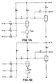
- FIGS. 1 A and 1 B The basic logic circuit is shown in FIGS. 1 A and 1 B, it constitutes an AND gate from which a logic family of a type can be developed which will be called DTTL (Diode Transistor Transistor Logic).
- DTTL Diode Transistor Transistor Logic
- It includes low barrier Schottky diodes D1, D2; ... Dn.
- the cathodes of these diodes constitute the input terminals IN1, IN2 ... INn of the circuit on which are applied input signals A, B ... etc.
- the anodes are connected in common to the base of an NPN type input transistor T1, on the one hand and via an implanted resistor R1 at the supply voltage + V on the other hand.
- the voltage + V is chosen to be equal to 1.7 volts.
- the collector of transistor T1 is connected to the supply voltage + V by an implanted resistor R2 and its emitter is connected to ground by a circuit 1.
- the collector of transistor T1 is connected to the base of an output transistor T2 inverter.
- the emitter of transistor T2 is connected to ground and its collector is connected to the supply voltage + V by an implanted resistor R3.
- the circuit output signal is taken from the output terminal OUT at the collector of transistor T2.
- Two anti-saturation Schottky diodes S1 and S2 with high barrier are disposed between the collector and the base of the transistors T1 and T2.
- this circuit is that the emitter of transistor T1 is connected to ground via circuit 1.
- This circuit can be constituted by a reference voltage source VREF equal to the emitter collector voltage VCE of an NPN transistor, ie 0.3 volts, as shown in FIG. 1 A, or it can be constituted by another logic circuit whose the output signal X is applied to the emitter of transistor T1 as shown in FIG. 1 B.
- the or the corresponding input diodes D1 to Dn are polarized in the forward direction and consequently the transistor T1 is blocked.
- the voltage at the collector of T1 being at the high level, the transistor T2 is conductive and the level of the output signal is low equal to the collector-emitter voltage VCE of the transistor T2.
- the basic circuit of FIG. 1 A therefore performs the AND function of the signals applied to its inputs.
- the circuit of FIG. 2 comprises two input transistors T1-1 and T1-2, provided with anti-saturation Schottky diodes (which is symbolically represented by an S in the diagram of the transistor) and four Schottky diodes of low barrier input D1, D2, D3 and D4.
- the diodes D1 and D2 receive on their cathodes two input signals A and B and have their anodes connected to the base of the transistor T1-1.
- the diodes D3 and D4 receive on their cathodes two input signals C and D and have their anodes connected to the base of the transistor T1-2.
- T1-1 and T1-2 are connected to the supply voltage + V by resistors R1-1 and R1-2 respectively.
- the collectors of T1-1 and T1-2 are connected in common and connected to the supply voltage + V by a resistor R2 and are connected to the base of the inverter output transistor T2, the collector of which is connected to the voltage + V by resistor R3 and the transmitter is connected to ground, as in the circuit of Figure 1 A or 1 B.
- the voltage on the emitters of transistors T1-1 and T1-2 is equal to VREF or that X is at the low level.
- the transistors T1-1 and T1- 1 are blocked and therefore the output transistor T2 is conductive so the output signal is at the low level.
- the transistors T1-1 and T1-2 are conductive and therefore T2 is blocked, therefore the output signal is at the high level.
- T1-1 is blocked and T1-2 is conductive of which T2 is blocked and the output signal is level high.
- T1 ⁇ 2 If one or other of the signals C or D is at the low level and A and B are at the high level T1 ⁇ 2 is blocked and T1-1 is conductive therefore T2 is blocked and the output signal is at the high level .
- the circuit of FIG. 2 performs the function X (AB + CD) or AB + CD.
- the circuit of FIG. 3 is identical to that of FIG. 2 except that the emitters of the two transistors T1-1 and T1-2 are not connected together but receive the output signals X and Y coming from other logic circuits, and consequently it performs the logic function ABX + CDY.
- the circuit of Figure 4 consists of two circuits of Figure 1 B. It includes two input transistors T1-1 and T1-2 and two output transistors T2-1 and T2-2.
- the input transistors T1-1 and T1-2 have their bases connected to the anodes of the input diodes D1, D2 and D3, D4 as in the arrangement of FIG. 3.
- the cathodes of the diodes D1 to D4 receive the signals input A, B, C and D respectively.
- the anodes of diodes D1 and D2 are connected to the supply voltage + V by the resistor R1-1 and the anodes of the diodes D3 and D4 are connected to the supply voltage + V by the resistor R1-2.
- the collector of transistor T1-1 is connected to the base of the first output transistor T2-1 and the collector of transistor T1-2 is connected to the base of the second output transistor T2-2.
- the collectors of the transistors T2-1 and T2-2 are connected in common to the voltage + V by a resistor R3.
- the output OUT is taken to the common collectors of the two output transistors so that the circuit of FIG. 4 performs the logic function (ABX). (CD Y).
- a microchip comprising cells of the universal type arranged in a conventional manner in rows and columns.
- cells of the universal type arranged in a conventional manner in rows and columns.
- semiconductive elements transistor diodes and resistors which are not connected to each other.
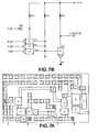
- the cell contains five low barrier Schottky diodes D11 to D15, the cathodes of which constitute the inputs of the logic circuits, seven resistors located R11 to R17 and four transistors T11 to T14 among which T11 is a dual emitter transistor.
- FIG. 5B constitutes a view of the cell in the plane of the first metallization level.
- Their arrangement in the silicon of the chip is such that the connections between the elements are of minimum length, whatever the type of family circuit which will be produced in the cell.
- a grid of 9xl3 possible vias is provided in each cell. The vias are represented by squares in Figure 5B.
- the anodes of the Schottky diodes are identified by the letter A and the cathodes by the letter K.
- the bases, emitters and collectors of the transistors are identified by the letters B, E and C respectively.
- the anti-saturation Schottky diodes, mounted between the collector and the base of the transistors T11 to T14 are not shown.
- each cell is personalized by arranging the appropriate contacts for the pre-diffused elements and wiring at the first metallization level to connect the elements so that the cell performs a logical function with accessible 1/0 inputs-outputs.
- LST Logical Service Terminal
- the wiring between the cells is then carried out at the second and third metallization levels.
- the first step in designing a logic network is to define the first level of metallization.
- a primary LST and several secondary terminals are defined.
- a conventional automatic wiring program defines the interconnections between the primary input / output terminals.
- a secondary terminal is chosen. Only one via among the total number of vias defined for an I / O input / output terminal is used, the others not being made in the final cell thus personalized, the cabling can pass on these unused vias without making contact at the input / output terminals.
- This process gives more freedom for wiring and allows the length, capacity and resistance of the conductors which interconnect the cells to be limited.
- All the logical functions which it is possible to carry out from one or more universal cells are pre-wired to constitute, in an automatic design system assisted by CAD computer, a library of cells which will be available to the designer of logical networks. . These cells can be arranged by automatic positioning and wiring programs to form the network, in accordance with the teachings of European patent 79103921.7 (EP-A-0 011 700).
- FIG. 6A are represented by the shaded parts, the connections necessary to personalize a cell in order to carry out the function of the circuit of FIG. 1B with four inputs.
- FIG. 6B The equivalent diagram is given in FIG. 6B in which the semiconductor elements of the Figure 5B cell have been referenced by the same numbers.
- This cell comprises an input diode D12 receiving the logic signal A and three input transistors constituted by the dual emitter transistor T11 and, the transistor T13 whose collector is connected to the collector of T12, as shown in dotted lines in the figure. 5B.
- FIG. 8A are shown the connections necessary for the personalization of a cell carrying out the function AB + CDE, when the emitters of the transistors T13 and T12 are connected to the reference voltage as shown in the diagram equivalent to FIG. 8B.
- the cell of FIG. 8A performs the function X AB + Y CDE.
- the transmitters of T13 and T14 are connected together and receive the output X from another cell, the cell in FIG. 8A performs the function X (AB + CDE).
- FIG. 9A the connections necessary for the personalization of a cell performing the function (A + B + C) D.
- the equivalent diagram is given in FIG. 9B.
- FIG. 10A An example of connections which make it possible to produce a rocker is shown in FIG. 10A.
- the equivalent diagram is given in FIG. 10B.
- circuits By connecting several cells together, circuits, performing complex logic functions, which are often used in logic networks can be created and put in the circuit library available to the designer.
- multiplier / adder circuit produced with three cells, which can enter into the constitution of a multiplier as shown in FIG. 11.
- This multiplier realizes the multiplication of a multiplicand X3 X2 X1 XO and a multiplier Y3 Y2 Y1 YO to supply the product P7 P6 P5 P4 P3 P2 P1 PO as shown in the figure.
- the adder ADD as shown in FIG. 12B comprises a first exclusive OR circuit 10 comprising the transistors T12 and T13 of the cell, the diodes D12 and D15, the output transistor T14 and the resistors R12, R13, R15 and R16.
- This circuit receives as inputs: the factor Pi on the transmitter of T12 and the cathode of the diode D12 and the transfer Ci on the transmitter of T13 and the cathode of D15.
- the anode of diode D12 is connected to the base of T13, and the anode of diode D15 is connected to the base of T12.
- the common collector of the transistors T12 and T13 is connected by the resistor R15 to the voltage + V and is connected at the base to the output transistor T14.
- the transmitter of T14 is connected to ground and its collector is connected to the voltage + V by the resistor R16.
- This circuit constitutes a conventional exclusive OR circuit, therefore the output to the collector of T14 is equal to Pi 0 Ci.
- a second exclusive OR circuit 12 with three inputs is produced in a second cell, and has an arrangement similar to that of circuit 10.
- Transistors T13 and T14 are used, as well as the transistor T11 with double emitter, on which the input signals X and Y are applied.
- the emitter of transistor T13 is connected to the output Pi 0 Ci of cell 10.
- Diode D12 has its cathode connected to the emitter of T13 and its anode connected to the base of T11.
- Diode D15 has its cathode connected to one of the emitters of T11 and its anode connected to the base of T13 and diode D14 has its cathode connected to the other emitter of T11 and its anode connected to the base of T13.
- the output transistor is arranged as in cell 10. So at the output of cell 12, taken at the collector of transistor T14, we get:
- the circuit of cell 14 is identical to that of FIG. 8B and receives Pi, Ci on the one hand, and Pi O Ci, X and Y on the other hand.
- the dotted lines represent the connections at the second metallization level, made in the vertical wiring channels and allows both interconnect the cells and bring them the input signals X, Y, Pi and Ci.
- This type of complex function has been shown, by way of example, but it is obvious that we can consider many others, for example, parity trees made up of exclusive OR circuits can be made using eight cells, a one bit multiplier can be made in three cells, a carry-over prediction circuit for an adder 4 bits can be realized in four cells.
- the universal type cell shown in FIG. 5B in which the circuits of the DTTL family can be made up makes it possible to design logic networks having a power x performance product improved compared to logic networks made up of conventional NON AND cells. Indeed, many reversing stages are eliminated and thus the paths are shortened.
Abstract
Description
La présente invention concerne un circuit logique de base à partir duquel peut être développée une famille de circuits logiques qui permet de réaliser des réseaux logiques à très haute densité.The present invention relates to a basic logic circuit from which a family of logic circuits can be developed which makes it possible to produce very high density logic networks.
Actuellement, les systèmes de traitement de l'information sont en grande partie constitués de réseaux logiques prédiffusés. Pour diminuer le coût de tels systèmes, il faut faciliter la conception de ces réseaux.Currently, information processing systems are largely made up of pre-broadcast logical networks. To reduce the cost of such systems, it is necessary to facilitate the design of these networks.
Pour ce fair, on peut réaliser des réseaux à base de cellules universelles du type de celles décrites dans la demande de brevet français publiée sous le numéro 2 441 969.To do this, it is possible to make networks based on universal cells of the type described in the French patent application published under the
Cette cellule est réalisée à partir de circuits logique type ECL (Emitter Coupled Logic), et en conséquence son utilisation est réservée à la constitution de réseaux exigeant des vitesses de fonctionnement élevées sans nécessiter une grande densité d'intégration.This cell is made from logic circuits type ECL (Emitter Coupled Logic), and consequently its use is reserved for the constitution of networks requiring high operating speeds without requiring a high density of integration.
Généralement, pour ce type d'application, on utilise des microplaquettes dans lesquelles sont diffusées des cellules de base réalisant une fonction logique élémentaire, par exemple, NON ET. La microplaquette est ensuite personnalisée, c'est-à-dire que les cellules sont connectées entre elles, de façon appropriée pour constituer le réseau désiré.Generally, for this type of application, microchips are used in which are diffused basic cells performing an elementary logic function, for example, NAND. The microchip is then personalized, that is to say that the cells are connected together, in an appropriate manner to constitute the desired network.
La cellule de base comportant une porte TTL (Transistor-Transistor Logic) du type décrit dans le brevet français publié sous le numéro 2 234 713 a l'inconvénient d'être lente et ne permet pas d'obtenir une densité suffisamment élevée. En effet, la réalisation de certaines fonctions à partir de cette porte NON ET nécessite un grand nombre de cellules.The basic cell comprising a TTL (Transistor-Transistor Logic) gate of the type described in the French patent published under
La cellule de base comportant une porte DTL (Diode Transistor Logic), outre l'inconvénient de la faible densité, présente celui d'avoir une faible immunité au bruit à cause du faible niveau de commutation.The basic cell comprising a DTL (Diode Transistor Logic) gate, in addition to the disadvantage of the low density, has that of having low noise immunity due to the low switching level.
Les technologies actuelles permettent de réaliser des réseaux intégrés avec quatre niveaux de métallisation. En conséquence, il n'est plus nécessaire que les cellules constitutives du réseau, généralement disposées en matrice, soient séparées pour laisser la place aux connexions intercel- lules, celles-ci se faisant désormais aux différents niveaux de métallisation. Par exemple, les éléments de la cellule peuvent être connectés au premier niveau, les canaux de cablage verticaux peuvent être prévus au second niveau, et les canaux de cablage horizontaux peuvent être prévus au troisième niveau.Current technologies allow for integrated networks with four metallization levels. Consequently, it is no longer necessary for the constituent cells of the network, generally arranged in a matrix, to be separated to make room for the inter-cell connections, these now being made at the different metallization levels. For example, the elements of the cell can be connected at the first level, the vertical wiring channels can be provided at the second level, and the horizontal wiring channels can be provided at the third level.
La surface de la cellule est déterminée en fonction du nombre de cellules à câbler par le pas de répétition des canaux de cablage horizontaux et verticaux.The cell surface is determined according to the number of cells to be wired by the repetition step of the horizontal and vertical wiring channels.
En conséquence, on ne peut plus augmenter la densité d'intégration des réseaux logiques constitués à base de portes NON ET classiques du fait que chaque cellule doit occuper une surface déterminée.Consequently, it is no longer possible to increase the integration density of the logical networks constituted on the basis of conventional NAND gates because each cell must occupy a determined surface.
Le circuit décrit dans l'article publié dans l'IBM Technical Disclosure Bulletin, vol. 25, no. 1, juin 1982, page 334 est un circuit qui contrairement aux circuits DTL classiques est constitué à l'aide de diodes de Schottky à barrière élevée. A cause de la chute de tension élevée dans ces diodes, il est nécessaire de connecter l'émetteur du transistor d'entrée à une tension de référence de valeur choisie très précisément pour permettre le blocage des transistors T1 et T2. Ce circuit présente une immunité au bruit qui est compatible--avec celle des circuits T2L classiques mais pas meilleure.The circuit described in the article published in the IBM Technical Disclosure Bulletin, vol. 25, no. 1, June 1982, page 334 is a circuit which, unlike conventional DTL circuits, is formed using high barrier Schottky diodes. Because of the high voltage drop in these diodes, it is necessary to connect the emitter of the input transistor to a reference voltage of value chosen very precisely to allow the blocking of transistors T1 and T2. This circuit has a noise immunity which is compatible - with that of conventional T2L circuits but not better.
Un objet de la présente invention est donc de réaliser un circuit logique de base qui permette de constituer une cellule de type universel capable de réaliser un grand nombre de fonctions.An object of the present invention is therefore to provide a basic logic circuit which makes it possible to constitute a universal type cell capable of performing a large number of functions.
Un autre objet de la présente invention est de réaliser un tel circuit logique qui permette d'améliorer le facteur coût/performance des microplaquettes de réseaux logiques.Another object of the present invention is to provide such a logic circuit which makes it possible to improve the cost / performance factor of the chips of logic networks.
Un autre objet de la présente invention est de réaliser un tel circuit qui permette de constituer des réseaux logiques à haute densité d'intégration avec de faibles alimentations de tension.Another object of the present invention is to provide such a circuit which makes it possible to form logic networks with high integration density with low voltage supplies.
Le circuit élémentaire conforme à la présente invention permet de réaliser une fonction logique de base à partir de n signaux d'entrée A, B ... et potentiellement d'un signal d'entrée supplémentaire X. Il comprend n diodes d'entrée de Schottky à faible barrière (D1 à DN) ayant des premières électrodes recevant chacune un des n signaux d'entrée et des secondes électrodes connectées à un noeud commun relié par une résistance à une première alimentation de tension de faible valeur (+1,7 volt), et un transistor d'entrée qui a sa base connectée au noeud commun, dont le collecteur est connecté par une résistance à la première tension d'alimentation et dont l'émetteur peut être connecté à une tension de référence dont la valeur est égale au niveau bas des signaux d'entrée pour obtenir un circuit présentant une bonne immunité au bruit, ou pouvant recevoir un signal d'entrée supplémentaire X lorsque l'immunité au bruit n'est pas critique. Un transistor inverseur de sortie a sa base connectée au collecteur du transistor d'entrée, son émetteur relié à une seconde alimentation de tension (0 volt) et son collecteur connecté par une résistance à la première tension d'alimentation, de telle sorte que le niveau logique obtenu au collecteur du transistor de sortie représente la fonction (AB C ...) ou X (AB ...) suivant que l'émetteur du transistor d'entrée est connecté à la tension de référence ou reçoit le signal d'entrée supplémentaire.The elementary circuit according to the present invention makes it possible to carry out a basic logic function from n input signals A, B ... and potentially from an additional input signal X. It comprises n input diodes of Low barrier Schottky (D1 to DN) having first electrodes each receiving one of the n input signals and second electrodes connected to a common node connected by a resistor to a first low voltage power supply (+1.7 volts ), and an input transistor which has its base connected to the common node, whose collector is connected by a resistor to the first supply voltage and whose emitter can be connected to a reference voltage whose value is equal at the low level of the input signals to obtain a circuit having good noise immunity, or capable of receiving an additional input signal X when the noise immunity is not critical. An output inverting transistor has its base connected to the collector of the input transistor, its emitter connected to a second voltage supply (0 volts) and its collector connected by a resistor to the first supply voltage, so that the logic level obtained at the collector of the output transistor represents the function (AB C ...) or X (AB ...) depending on whether the emitter of the input transistor is connected to the reference voltage or receives the signal additional entrance.
A partir de ce circuit élémentaire, on peut construire une famille de circuits logiques qui pourra être appelée DTTL (Diode Transistor Transistor Logic) car les circuits se comportent à la fois comme des circuits DTL et des circuits TTL. Chaque circuit logique peut être constitué de plusieurs circuits élémentaires ou peut être constitué en disposant dans un circuit élémentaire plusieurs transistors d'entrée. Le signal d'entrée supplémentaire peut être appliqué sur tous les émetteurs de transistors d'entrée ou des signaux supplémentaires différents peuvent être appliqués aux émetteurs des transistors. Les bases des transistors d'entrée sont connectées à une ou plusieurs diodes d'entrée sur lesquelles sont appliqués les signaux d'entrée (A, B, C, D ...).From this elementary circuit, one can build a family of logic circuits which could be called DTTL (Diode Transistor Transistor Logic) because the circuits behave both as DTL circuits and TTL circuits. Each logic circuit can be made up of more several elementary circuits or can be constituted by arranging in an elementary circuit several input transistors. The additional input signal can be applied to all the emitters of the input transistors or different additional signals can be applied to the emitters of the transistors. The bases of the input transistors are connected to one or more input diodes on which the input signals are applied (A, B, C, D ...).
Les circuits logiques de la famille sont constitués dans une cellule universelle comportant des éléments semi-conducteurs: diodes, transistors et résistances implantées, prédiffusés, de telle sorte que par cablage au premier niveau de métallisation des éléments appropriés, on puisse constituer tous les circuits de la famille. Les cellules sont ensuite interconnectées entre elles aux second et troisième niveaux de métallisation pour former des réseaux logiques très denses et très performants.The logic circuits of the family are constituted in a universal cell comprising semiconductor elements: diodes, transistors and resistors implanted, pre-diffused, so that by wiring at the first level of metallization of the appropriate elements, it is possible to constitute all the circuits of family. The cells are then interconnected with each other at the second and third metallization levels to form very dense and very efficient logic networks.
- Les figures 1A et 1 B représentent les circuits élémentaires DTTL conformes à la présente invention.FIGS. 1A and 1B represent the elementary circuits DTTL in accordance with the present invention.
- La figure 2 représente un premier circuit de la famille logique DTTL réalisant la fonction logique X(AB+CD) ou (AB+CD).FIG. 2 represents a first circuit of the DTTL logic family performing the logic function X (AB + CD) or (AB + CD).
- La figure 3 représente un second circuit de la famille logique DTTL réalisant la fonction logique ABX+CDY.FIG. 3 represents a second circuit of the DTTL logic family realizing the ABX + CDY logic function.
- La figure 4 représente un troisième circuit de la famille logique DTTL réalisant la fonction logique (ABX).(CDY).FIG. 4 represents a third circuit of the DTTL logic family performing the logic function (ABX). (CDY).
- Les figures 5A et 5B représentent une cellule universelle permettant de constituer les circuits de la famille logique.FIGS. 5A and 5B represent a universal cell making it possible to constitute the circuits of the logic family.
- Les figures 6A à 10A représentent les connexions nécessaires pour constituer dans la cellule les circuits des 6B à 10B.FIGS. 6A to 10A represent the connections necessary to constitute in the cell the circuits of 6B to 10B.
- La figure 11 représente le schéma global d'un multiplicateur.Figure 11 shows the overall diagram of a multiplier.
- La figure 12A représente les connexions nécessaires pour réaliser en trois cellules le circuit de multiplication de la figure 12B, constituant un élément du multiplicateur de la figure 11.FIG. 12A represents the connections necessary to make the multiplication circuit of FIG. 12B in three cells, constituting an element of the multiplier of FIG. 11.
Le circuit logique de base est représenté sur les figures 1 A et 1 B, il constitue une porte ET à partir de laquelle pourra être développée une famille logique d'un type qui sera appelé DTTL (Diode Transistor Transistor Logic).The basic logic circuit is shown in FIGS. 1 A and 1 B, it constitutes an AND gate from which a logic family of a type can be developed which will be called DTTL (Diode Transistor Transistor Logic).
Il comprend des diodes de Schottky à faible barrière D1, D2;...Dn. Les cathodes de ces diodes constituent les bornes d'entrée IN1, IN2...INn du circuit sur lesquelles sont appliqués des signaux d'entrée A, B ...etc.It includes low barrier Schottky diodes D1, D2; ... Dn. The cathodes of these diodes constitute the input terminals IN1, IN2 ... INn of the circuit on which are applied input signals A, B ... etc.
Les anodes sont connectées en commun à la base d'un transistor d'entrée de typ NPN T1, d'une part et par l'intermédiaire d'une résistance implanté R1 à la tension d'alimentation +V d'autre part. Dans un mode de réalisation préféré, la tension +V est choisie égale à 1,7 volts.The anodes are connected in common to the base of an NPN type input transistor T1, on the one hand and via an implanted resistor R1 at the supply voltage + V on the other hand. In a preferred embodiment, the voltage + V is chosen to be equal to 1.7 volts.
Le collecteur du transistor T1 est connecté à la tension d'alimentation +V par une résistance implantée R2 et son émetteur est connecté à la masse par un circuit 1. Le collecteur du transistor T1 est connecté à la base d'un transistor de sortie T2 inverseur.The collector of transistor T1 is connected to the supply voltage + V by an implanted resistor R2 and its emitter is connected to ground by a
L'émetteur du transistor T2 est connecté à la masse et son collecteur est connecté à la tension d'alimentation +V par une résistance implantée R3.The emitter of transistor T2 is connected to ground and its collector is connected to the supply voltage + V by an implanted resistor R3.
Le signal de sortie du circuit est pris à la borne de sortie OUT au collecteur du transistor T2.The circuit output signal is taken from the output terminal OUT at the collector of transistor T2.
Deux diodes de Schottky d'antisaturation S1 et S2 à barrière élevée sont disposées entre le collecteur et la base des transistors T1 et T2.Two anti-saturation Schottky diodes S1 and S2 with high barrier are disposed between the collector and the base of the transistors T1 and T2.
La particularité de ce circuit tient au fait que l'émetteur du transistor T1 est connecté à la masse par l'intermédiaire du circuit 1.The particularity of this circuit is that the emitter of transistor T1 is connected to ground via
Ce circuit peut être constitué par une source de tension de référence VREF égale à la tension collecteur émetteur VCE d'un transistor NPN soit 0,3 volt, comme représenté sur la figure 1 A, ou il peut être constitué par un autre circuit logique dont le signal de sortie X est appliqué à l'émetteur du transistor T1 comme représenté sur la figure 1 B.This circuit can be constituted by a reference voltage source VREF equal to the emitter collector voltage VCE of an NPN transistor, ie 0.3 volts, as shown in FIG. 1 A, or it can be constituted by another logic circuit whose the output signal X is applied to the emitter of transistor T1 as shown in FIG. 1 B.
Ainsi, on peut constituer des ensembles logiques de type cascode comme cela sera décrit ultérieurement, et de ce fait augmenter la puissance logique du circuit de base de la figure 1 A.Thus, it is possible to constitute logical sets of cascode type as will be described later, and thereby increase the logical power of the basic circuit of FIG. 1 A.
Lorsqu'au moins un des signaux sur les entrées IN1 à INn est à un niveau bas, c'est-à-dire inférieur à un seuil Vt de préférence égal à 0,3 volt soit la tension VCE d'un transistor, la ou les diodes d'entrée D1 à Dn correspondantes sont polarisées dans le sens direct et en conséquence le transistor T1 est bloqué. La tension au collecteur de T1 étant au niveau haut, le transistor T2 est conducteur et le niveau du signal de sortie est bas égal à la tension collecteur-émetteur VCE du transistor T2.When at least one of the signals on the inputs IN1 to INn is at a low level, that is to say less than a threshold Vt preferably equal to 0.3 volts, ie the voltage VCE of a transistor, the or the corresponding input diodes D1 to Dn are polarized in the forward direction and consequently the transistor T1 is blocked. The voltage at the collector of T1 being at the high level, the transistor T2 is conductive and the level of the output signal is low equal to the collector-emitter voltage VCE of the transistor T2.
Lorsque les signaux sur les entrées IN1 à INn sont à un niveau haut, les diodes d'entrée sont bloquées et le transistor T1 est conducteur, ce qui provoque le blocage du transistor T2 le niveau du signal de sortie est donc haut.When the signals on the inputs IN1 to INn are at a high level, the input diodes are blocked and the transistor T1 is conductive, which causes the blocking of the transistor T2 the level of the output signal is therefore high.
Le circuit de base de la figure 1 A réalise donc la fonction ET des signaux appliqués à ses entrées.The basic circuit of FIG. 1 A therefore performs the AND function of the signals applied to its inputs.
La tension de seuil est égal à:
- VREF+VBE(T1 )-VS=0,3+0,8-0,3=0,8 volt
- VBE (T1) représente la tension base émetteur du transistor T1 et la tension VS représente la tension aux bornes d'une diode de Schottky lorsqu'elle est polarisée dans le sens direct.
- L'immunité au bruit VI M du circuit est égal à:
- VT-VIN=VT-VCE=0,5 volt
- VREF + VBE (T1) -VS = 0.3 + 0.8-0.3 = 0.8 volt
- VBE (T1) represents the base emitter voltage of transistor T1 and the voltage VS represents the voltage across a Schottky diode when it is polarized in the forward direction.
- The immunity to noise VI M of the circuit is equal to:
- VT-VIN = VT-VCE = 0.5 volt
Elle est donc deux fois supérieure à l'immunité au bruit des circuits conventionnels de type DTL ou TTL.It is therefore twice as good as the noise immunity of conventional DTL or TTL circuits.
Ceci permet d'augmenter de façon importante le nombre des entrées et sorties et de faciliter la conception des réseaux logiques.This makes it possible to significantly increase the number of inputs and outputs and to facilitate the design of logical networks.
Le fonctionnement du circuit de la figure 1 B est le suivant:
- Le signal X représente le résultat d'une fonction logique réalisée
par le circuit 1. Ce circuit étant du même type que le circuit de la figure 1 A, le niveau du signal X est soit égal à VCE (niveau bas) soit égal àenviron 1,7 volt (niveau haut). - Si X a un niveau bas égal à VCE, le circuit de la figure 1 B fonctionne de la même façon que celui de la figure 1A et fournit un signal de sortie qui dépend des niveaux sur les entrées IN1 à INn.
- Si X a un niveau haut, quels que soient les niveaux des signaux sur les entrées IN1 à INn, le transistor T1 ne sera jamais conducteur et en conséquence la sortie sera toujours au niveau bas.
- Signal X represents the result of a logic function performed by
circuit 1. This circuit being same type as the circuit of figure 1 A, the level of the signal X is either equal to VCE (low level) or equal to approximately 1,7 volt (high level). - If X has a low level equal to VCE, the circuit of FIG. 1B operates in the same way as that of FIG. 1A and provides an output signal which depends on the levels on the inputs IN1 to INn.
- If X has a high level, whatever the signal levels on the inputs IN1 to INn, the transistor T1 will never be conductive and consequently the output will always be at the low level.
Le circuit de la figure 1 B réalise donc la fonction logique:
- (AB ...) X
- (AB ...) X
On va maintenant montrer comment en partant de ce circuit de base on peut développer une famille de circuits logiques.We will now show how, starting from this basic circuit, we can develop a family of logic circuits.
Trois circuits de la famille sont représentés sur les figures 2, 3 et 4 à titre d'exemple.Three family circuits are shown in Figures 2, 3 and 4 by way of example.
Le circuit de la figure 2 comporte deux transistors d'entrée T1-1 et T1-2, munis de diodes de Schottky d'antisaturation (ce qui est représenté symboliquement par un S dans le schéma du transistor) et quatre diodes de Schottky d'entrée à faible barrière D1, D2, D3 et D4.The circuit of FIG. 2 comprises two input transistors T1-1 and T1-2, provided with anti-saturation Schottky diodes (which is symbolically represented by an S in the diagram of the transistor) and four Schottky diodes of low barrier input D1, D2, D3 and D4.
Les diodes D1 et D2 reçoivent sur leurs cathodes deux signaux d'entrée A et B et ont leurs anodes connectées à la base du transistor T1-1. Les diodes D3 et D4 reçoivent sur leurs cathodes deux signaux d'entrée C et D et ont leurs anodes connectées à la base du transistor T1-2.The diodes D1 and D2 receive on their cathodes two input signals A and B and have their anodes connected to the base of the transistor T1-1. The diodes D3 and D4 receive on their cathodes two input signals C and D and have their anodes connected to the base of the transistor T1-2.
Les bases de T1-1 et de T1-2 sont connectées à la tension d'alimentation +V par des résistances R1-1 et R1-2 respectivement. Les collecteurs de T1-1 et T1-2 sont connectés en commun et reliés à la tension d'alimentation +V par une résistance R2 et sont connectés à la base du transistor de sortie inverseur T2, dont le collecteur est connecté à la tension +V par la résistance R3 et l'émetteur est connecté à la masse, comme dans le circuit de la figure 1 A ou 1 B.The bases of T1-1 and T1-2 are connected to the supply voltage + V by resistors R1-1 and R1-2 respectively. The collectors of T1-1 and T1-2 are connected in common and connected to the supply voltage + V by a resistor R2 and are connected to the base of the inverter output transistor T2, the collector of which is connected to the voltage + V by resistor R3 and the transmitter is connected to ground, as in the circuit of Figure 1 A or 1 B.
Supposons que la tension sur les émetteurs des transistors T1-1 et T1-2 soit égale à VREF ou que X soit au niveau bas.Suppose that the voltage on the emitters of transistors T1-1 and T1-2 is equal to VREF or that X is at the low level.
Si l'un des signaux d'entrée sur A et B et sur C et D est au niveau bas ou que tous les signaux d'entrée A, B, C et D sont au niveau bas, les transistors T1-1 et T1-1 sont bloqués et donc le transistor de sortie T2 est conducteur donc le signal de sortie est au niveau bas.If one of the input signals on A and B and on C and D is at the low level or if all the input signals A, B, C and D are on the low level, the transistors T1-1 and T1- 1 are blocked and therefore the output transistor T2 is conductive so the output signal is at the low level.
Si les signaux d'entrée A, B, C et D sont au niveau haut, les transistors T1-1 et T1-2 sont conducteurs et donc T2 est bloqué, donc le signal de sortie est au niveau haut.If the input signals A, B, C and D are at the high level, the transistors T1-1 and T1-2 are conductive and therefore T2 is blocked, therefore the output signal is at the high level.
Si l'un ou l'autre des signaux A ou B est au niveau bas et que C et D sont au niveau haut, T1-1 est bloqué et T1-2 est conducteur dont T2 est bloqué et le signal de sortie est au niveau haut.If either signal A or B is low and C and D are high, T1-1 is blocked and T1-2 is conductive of which T2 is blocked and the output signal is level high.
Si l'un ou l'autre des signaux C ou D est au niveau bas et que A et B sont au niveau haut T1~2 est bloqué et T1-1 est conducteur donc T2 est bloqué et le signal de sortie est au niveau haut.If one or other of the signals C or D is at the low level and A and B are at the
Si par contre X est au niveau haut, quels que soient les niveaux des signaux d'entrée A, B, C et D, les transistors T1-1 et T1-2 seront toujours bloqués et le transistor T2 sera conducteur. Le niveau du signal de sortie sera bas.If on the other hand X is at the high level, whatever the levels of the input signals A, B, C and D, the transistors T1-1 and T1-2 will always be blocked and the transistor T2 will be conductive. The output signal level will be low.
En conséquence suivant que les émetteurs des transistors T1-1 et T1-2 sont connectés à la sortie X d'un circuit logique ou à la tension VREF, le circuit de la figure 2 réalise la fonction X (AB+CD) ou AB+CD.Consequently, depending on whether the emitters of the transistors T1-1 and T1-2 are connected to the output X of a logic circuit or to the voltage VREF, the circuit of FIG. 2 performs the function X (AB + CD) or AB + CD.
Le circuit de la figure 3 est identique à celui de la figure 2 sauf que les émetteurs des deux transistors T1-1 et T1-2 ne sont pas reliés ensemble mais reçoivent les signaux de sortie X et Y venant d'autres circuits logiques, et en conséquence il réalise la fonction logique ABX+CDY.The circuit of FIG. 3 is identical to that of FIG. 2 except that the emitters of the two transistors T1-1 and T1-2 are not connected together but receive the output signals X and Y coming from other logic circuits, and consequently it performs the logic function ABX + CDY.
Le circuit de la figure 4 est constitué de deux circuits de la figure 1 B. Il comporte deux transistors d'entrée T1-1 et T1-2 et deux transistors de sortie T2-1 et T2-2.The circuit of Figure 4 consists of two circuits of Figure 1 B. It includes two input transistors T1-1 and T1-2 and two output transistors T2-1 and T2-2.
Les transistors d'entrée T1-1 et T1-2 ont leurs bases reliées aux anodes des diodes d'entrée D1, D2 et D3, D4 comme dans l'arrangement de la figure 3. Les cathodes des diodes D1 à D4 reçoivent les signaux d'entrée A, B, C et D respectivement. Les anodes des diodes D1 et D2 sont connectées à la tension d'alimentation +V par la résistance R1-1 et les anodes des diodes D3 et D4 sont connectées à la tension d'alimentation +V par la résistance R1-2.The input transistors T1-1 and T1-2 have their bases connected to the anodes of the input diodes D1, D2 and D3, D4 as in the arrangement of FIG. 3. The cathodes of the diodes D1 to D4 receive the signals input A, B, C and D respectively. The anodes of diodes D1 and D2 are connected to the supply voltage + V by the resistor R1-1 and the anodes of the diodes D3 and D4 are connected to the supply voltage + V by the resistor R1-2.
Le collecteur du transistor T1-1 est connecté à la base du premier transistor de sortie T2-1 et le collecteur du transistor T1-2 est connecté à la base du second transistor de sortie T2-2. Les collecteurs des transistors T2-1 et T2-2 sont connectés en commun à la tension +V par une résistance R3.The collector of transistor T1-1 is connected to the base of the first output transistor T2-1 and the collector of transistor T1-2 is connected to the base of the second output transistor T2-2. The collectors of the transistors T2-1 and T2-2 are connected in common to the voltage + V by a resistor R3.
La sortie OUT est prise aux collecteurs communs des deux transistors de sortie de telle sorte que le circuit de la figure 4 réalise la fonction logique (ABX).(CD Y).The output OUT is taken to the common collectors of the two output transistors so that the circuit of FIG. 4 performs the logic function (ABX). (CD Y).
D'autres arrangements peuvent être constitués de telle sorte que le circuit de base des figures 1 A ou 1 B permette le développement de toute une famille de circuits logiques, qui en plus d'avoir l'avantage d'une très grande immunité au bruit permette de réaliser des ensembles logiques ayant une puissance logique accrue. En effet X et Y représentant une fonction complexe, c'est-à-dire étant le résultat d'une fonction logique quelconque de plusieurs variables d'entrée, on peut réaliser des réseaux logiques avec des connexions de longueur minimum en disposant plusieurs étages de circuits suivant une configuration de type cascode.Other arrangements can be made so that the basic circuit of Figures 1 A or 1 B allows the development of a whole family of logic circuits, which in addition to having the advantage of very high noise immunity allows for logical assemblies with increased logical power. Indeed X and Y representing a complex function, that is to say being the result of any logical function of several input variables, we can make logical networks with connections of minimum length by having several stages of circuits following a cascode type configuration.
Pour faciliter la conception de réseaux logiques à partir de cette famille logique DTTL, on utilise une microplaquette comprenant des cellules de type universel disposées de façon classique en rangées et colonnes. Dans chacune des cellules sont prédiffusés des éléments semi-conducteurs: diodes transistors et des résistances qui ne sont pas connectés entre eux.To facilitate the design of logic networks from this DTTL logic family, a microchip is used comprising cells of the universal type arranged in a conventional manner in rows and columns. In each of the cells are semiconductive elements: transistor diodes and resistors which are not connected to each other.
Par personnalisation de la microplaquette, c'est-à-dire par personnalisation de chaque cellule en connectant les éléments entre eux, pour que la cellule réalise une fonction déterminée et par connexion des cellules entre elles, le réseau logique désiré est constitué.By personalization of the chip, that is to say by personalization of each cell by connecting the elements together, so that the cell performs a determined function and by connecting the cells together, the desired logical network is formed.
Dans un mode de réalisation préféré, représenté sur la figure 5A, la cellule contient cinq diodes de Schottky à faible barrière D11 à D15, dont les cathodes constitueront les entrées des circuits logiques, sept résistances implantées R11 à R17 et quatre transistors T11 à T14 parmi lesquels T11 est un transistor à double émetteur.In a preferred embodiment, represented in FIG. 5A, the cell contains five low barrier Schottky diodes D11 to D15, the cathodes of which constitute the inputs of the logic circuits, seven resistors located R11 to R17 and four transistors T11 to T14 among which T11 is a dual emitter transistor.
Ces éléments sont prédiffusés de façon appropriée à l'intérieur de la cellule, comme représenté sur la figure 5B qui constitue une vue de la cellule dans le plan du premier niveau de métallisation. Leur disposition dans le silicium de la microplaquette est telle que les connexions entre les éléments soient de longueur minimum, quel que soit le type de circuit de la famille qui sera réalisé dans la cellule. Une grille de 9xl3 vias possibles est prévue dans chaque cellule. Les vias sont représentés par des carrés sur la figure 5B.These elements are appropriately pre-diffused inside the cell, as shown in FIG. 5B which constitutes a view of the cell in the plane of the first metallization level. Their arrangement in the silicon of the chip is such that the connections between the elements are of minimum length, whatever the type of family circuit which will be produced in the cell. A grid of 9xl3 possible vias is provided in each cell. The vias are represented by squares in Figure 5B.
Les anodes des diodes de Schottky sont repérées par la lettre A et les cathodes par la lettre K. Les bases, émetteurs et collecteurs des transistors sont repérés par les lettres B, E et C respectivement. Les diodes de Schottky d'antisaturation, montées entre le collecteur et la base des transistors T11 à T14 ne sont pas représentées.The anodes of the Schottky diodes are identified by the letter A and the cathodes by the letter K. The bases, emitters and collectors of the transistors are identified by the letters B, E and C respectively. The anti-saturation Schottky diodes, mounted between the collector and the base of the transistors T11 to T14 are not shown.
Afin de réaliser un réseau logique, chaque cellule est personalisée en disposant les contacts appropriés aux éléments prédiffusés et un cablage au premier niveau de métallisation pour connecter les éléments entre eux afin que la cellule réalise une fonction logique avec des entrées-sorties 1/0 accessibles par plusieurs bornes LST (Logic Service Terminal) disposées à des points appropriés dans la grille de 9 x 13 vias ainsi que cela est représenté sur les figures montrant quelques exemples de personnalisation.In order to create a logical network, each cell is personalized by arranging the appropriate contacts for the pre-diffused elements and wiring at the first metallization level to connect the elements so that the cell performs a logical function with accessible 1/0 inputs-outputs. by several LST (Logic Service Terminal) terminals arranged at appropriate points in the 9 x 13 vias grid as shown in the figures showing some examples of personalization.
Le cablage entre les cellules est ensuite réalisé aux second et troisième niveaux de métallisation.The wiring between the cells is then carried out at the second and third metallization levels.
Pour constituer le cablage global du réseau, vingt-quatre canaux de cablage sont disponibles pour chaque cellule:
- 9 canaux de cablage horizontaux au troisième niveau de métallisation,
- 13 canaux de cablage verticaux au second niveau de métallisation,
- 2 canaux de cablage horizontaux au premier niveau de métallisation, réservés à des lignes de commande.
- 9 horizontal wiring channels at the third metallization level,
- 13 vertical wiring channels at the second metallization level,
- 2 horizontal wiring channels at the first metallization level, reserved for control lines.
La première étape de la conception d'un réseau logique consiste à définir le premier niveau de métallisation.The first step in designing a logic network is to define the first level of metallization.
Pour chaque borne 1/0, on définit une borne LST primaire et plusieurs secondaires. Lorsque toutes les fonctions logiques différentes sont placées dans la grille de cellules sur la microplaquette, un programme de cablage automatique classique définit les interconnexions entre les bornes d'entrée/sortie primaires.For each 1/0 terminal, a primary LST and several secondary terminals are defined. When all the different logic functions are placed in the cell grid on the microchip, a conventional automatic wiring program defines the interconnections between the primary input / output terminals.
Lorsque le cablage est impossible, une borne secondaire est choisie. Seul un via parmi le nombre total de vias définis pour une borne d'entrée/ sortie I/O est utilisé, les autres n'étant pas réalisés dans la cellule finale ainsi personnalisée, les câblages peuvent passer sur ces vias non utilisés sans faire contact aux bornes d'entrée/sortie.When wiring is impossible, a secondary terminal is chosen. Only one via among the total number of vias defined for an I / O input / output terminal is used, the others not being made in the final cell thus personalized, the cabling can pass on these unused vias without making contact at the input / output terminals.
Ce procédé donne plus de liberté pour le cablage et permet de limiter la longueur, la capacité et la résistance des conducteurs qui interconnec- tent les cellules.This process gives more freedom for wiring and allows the length, capacity and resistance of the conductors which interconnect the cells to be limited.
Toutes les fonctions logiques qu'il est possible de réaliser à partir d'une ou plusieurs cellules universelles sont précâblées pour constituer, dans un système de conception automatique assisté par ordinateur CAD, une librairie de cellules qui sera à la disposition du concepteur de réseaux logiques. Ces cellules peuvent être arrangées par des programmes de mise en place automatique et de cablage pour former le réseau, conformément aux enseignements du brevet européen 79103921.7 (EP-A-0 011 700).All the logical functions which it is possible to carry out from one or more universal cells are pre-wired to constitute, in an automatic design system assisted by CAD computer, a library of cells which will be available to the designer of logical networks. . These cells can be arranged by automatic positioning and wiring programs to form the network, in accordance with the teachings of European patent 79103921.7 (EP-A-0 011 700).
De nombreuses fonctions peuvent être réalisées, une liste non exhaustive est donnée ci-après. Le cablage pour obtenir ces fonctions peut être réalisé facilement par l'homme de métier à partir de la description précédente. Un exemple de cablage pour certaines fonctions sera donné en référence aux figures 6 à 10.


Sur la figure 6A sont représentées par les parties ombrées, les connexions nécessaires pour personnaliser une cellule afin de réaliser la fonction du circuit de la figure 1 B avec quatre entrées.In FIG. 6A are represented by the shaded parts, the connections necessary to personalize a cell in order to carry out the function of the circuit of FIG. 1B with four inputs.
Le schéma équivalent est donné sur la figure 6B dans laquelle les éléments semi-conducteurs de la cellule de la figure 5B ont été référencés par les mêmes numéros.The equivalent diagram is given in FIG. 6B in which the semiconductor elements of the Figure 5B cell have been referenced by the same numbers.
De la même façon, sur la figure 7A, sont représentées les connexions nécessaires pour la personnalisation d'une cellule réalisant de la fonction A(B+C+D).In the same way, in FIG. 7A, the connections necessary for the personalization of a cell performing the function A (B + C + D) are represented.
Cette cellule comporte une diode d'entrée D12 recevant le signal logique A et trois transistors d'entrée constitués par le transistor à double émetteur T11 et, le transistor T13 dont le collecteur est relié au collecteur de T12, comme représenté en pointillés sur la figure 5B.This cell comprises an input diode D12 receiving the logic signal A and three input transistors constituted by the dual emitter transistor T11 and, the transistor T13 whose collector is connected to the collector of T12, as shown in dotted lines in the figure. 5B.
Sur la figure 8A sont représentées les connexions nécessaires pour la personnalisation d'une cellule réalisant la fonction AB+CDE, lorsque les émetteurs des transistors T13 et T12 sont connectés à la tension de référence comme représenté sur le schéma équivalent à la figure 8B. Lorsque l'émetteur de T13 reçoit la sortie X d'une autre cellule et l'émetteur de T12 reçoit la sortie Y d'une autre cellule, la cellule de la figure 8A réalise la fonction X AB+ Y CDE. Lorsque les émetteurs de T13 et T14 sont connectés ensemble et reçoivent la sortie X d'une autre cellule, la cellule de la figure 8A réalise la fonction X (AB+CDE).In FIG. 8A are shown the connections necessary for the personalization of a cell carrying out the function AB + CDE, when the emitters of the transistors T13 and T12 are connected to the reference voltage as shown in the diagram equivalent to FIG. 8B. When the transmitter of T13 receives the output X from another cell and the transmitter of T12 receives the output Y of another cell, the cell of FIG. 8A performs the function X AB + Y CDE. When the transmitters of T13 and T14 are connected together and receive the output X from another cell, the cell in FIG. 8A performs the function X (AB + CDE).
Sur la figure 9A sont représentées les connexions nécessaires pour la personnalisation d'une cellule réalisant fa fonction (A+B+C) D. Le schéma équivalent est donné sur la figure 9B.In FIG. 9A are shown the connections necessary for the personalization of a cell performing the function (A + B + C) D. The equivalent diagram is given in FIG. 9B.
De nombreuses autres configurations de cablage peuvent être envisagées pour réaliser une très grande variété de fonctions logiques ou autres circuits logiques tels que divers types de bascules.Many other wiring configurations can be envisaged to achieve a very wide variety of logic functions or other logic circuits such as various types of flip-flops.
Un exemple de connexions qui permettent de réaliser une bascule est représenté sur la figure 10A. Le schéma équivalent est donné sur la figure 10B.An example of connections which make it possible to produce a rocker is shown in FIG. 10A. The equivalent diagram is given in FIG. 10B.
En connectant ensemble plusieurs cellules, des circuits, réalisant des fonctions logiques complexes, qui sont souvent utilisés dans les réseaux logiques peuvent être constitués et mis dans la librairie de circuits à la disposition du concepteur.By connecting several cells together, circuits, performing complex logic functions, which are often used in logic networks can be created and put in the circuit library available to the designer.
A titre d'exemple, on montrera en référence aux figures un circuit multiplicateur/additionneur réalisé avec trois cellules, pouvant entrer dans la constitution d'un multiplicateur tel que représenté sur la figure 11. Ce multiplicateur réalise la multiplication d'un multiplicande X3 X2 X1 XO et d'un multiplicateur Y3 Y2 Y1 YO pour fournir le produit P7 P6 P5 P4 P3 P2 P1 PO comme indiqué sur la figure.By way of example, we will show with reference to the figures a multiplier / adder circuit produced with three cells, which can enter into the constitution of a multiplier as shown in FIG. 11. This multiplier realizes the multiplication of a multiplicand X3 X2 X1 XO and a multiplier Y3 Y2 Y1 YO to supply the product P7 P6 P5 P4 P3 P2 P1 PO as shown in the figure.
Il comprend des portes ET (représentées par des demi-cercles) et des additionneurs complets ou demi-additionneurs référencés ADD et 1/2 ADD. Cette disposition est classique et ne fait pas partie de la présente invention, elle n'est donnée que pour montrer comment pourra être utilisé le circuit de la figure qui représente un circuit multiplicateur comprenant le circuit ET et l'additionneur ADD recevant les produits X Y de deux bits des multiplicande et multiplicateur X et Y, le facteur Pi venant d'un additionneur ADD de l'étage supérieur et le report Ci venant de l'additionneur ADD de droite. Chaque additionneur génère les facteurs Po et Co qui constituent les facteurs Pi et Ci destinés à l'étage inférieur et à l'additionneur de gauche, comme on peut le voir sur la figure 11.It includes AND gates (represented by half-circles) and of full adders and half-adders referenced ADD and half ADD. This arrangement is conventional and does not form part of the present invention, it is given only to show how the circuit of the figure which represents a multiplier circuit comprising the AND circuit and the adder ADD receiving the products XY of can be used. two bits of the multiplicand and multiplier X and Y, the factor Pi coming from an ADD adder of the upper stage and the transfer Ci coming from the ADD adder on the right. Each adder generates the factors Po and Co which constitute the factors Pi and Ci intended for the lower stage and for the left adder, as can be seen in FIG. 11.
Les facteurs Po et Co sont les résultats des fonctions logiques suivantes:![]()
![]()
![]()
![]()
En conséquence, l'additionneur ADD comme représenté sur la figure 12B comprend un premier circuit OU exclusif 10 comportant les transistors T12 et T13 de la cellule, les diodes D12 et D15, le transistor de sortie T14 et les résistances R12, R13, R15 et R16.Consequently, the adder ADD as shown in FIG. 12B comprises a first exclusive OR
Ce circuit reçoit comme entrées: le facteur Pi sur l'émetteur de T12 et la cathode de la diode D12 et le report Ci sur l'émetteur de T13 et la cathode de D15.This circuit receives as inputs: the factor Pi on the transmitter of T12 and the cathode of the diode D12 and the transfer Ci on the transmitter of T13 and the cathode of D15.
L'anode de la diode D12 est connectée à la base de T13, et l'anode de la diode D15 est connectée à la base de T12. Les bases des transistors T12 et T13 sont connectées à la tension d'alimentation +V=1,7 volt par les résistances R12 et R13 respectivement. Le collecteur commun des transistors T12 et T13 est connecté par la résistance R15 à la tension +V et est connecté à la base au transistor de sortie T14. L'émetteur de T14 est connecté à la masse et son collecteur est connecté à la tension +V par la résistance R16.The anode of diode D12 is connected to the base of T13, and the anode of diode D15 is connected to the base of T12. The bases of the transistors T12 and T13 are connected to the supply voltage + V = 1.7 volts by the resistors R12 and R13 respectively. The common collector of the transistors T12 and T13 is connected by the resistor R15 to the voltage + V and is connected at the base to the output transistor T14. The transmitter of T14 is connected to ground and its collector is connected to the voltage + V by the resistor R16.
Ce circuit constitue un circuit OU exclusif classique, donc la sortie au collecteur de T14 est égale à Pi 0 Ci.This circuit constitutes a conventional exclusive OR circuit, therefore the output to the collector of T14 is equal to Pi 0 Ci.
Un second circuit OU exclusif 12 à trois entrées est réalisé dans une deuxième cellule, et comporte une disposition similaire à celle du circuit 10.A second exclusive OR
Il est fait usage des transistors T13 et T14 ainsi que du transistor T11 à double émetteur, sur lesquels sont appliqués les signaux d'entrée X et Y.Transistors T13 and T14 are used, as well as the transistor T11 with double emitter, on which the input signals X and Y are applied.
L'émetteur du transistor T13 est connecté à la sortie Pi 0 Ci de la cellule 10.The emitter of transistor T13 is connected to the output Pi 0 Ci of
La diode D12 a sa cathode connectée à l'émetteur de T13 et son anode connectée à la base de T11. La diode D15 a sa cathode connectée à un des émetteurs de T11 et son anode connectée à la base de T13 et la diode D14 a sa cathode connectée à l'autre émetteur de T11 et son anode connectée à la base de T13.Diode D12 has its cathode connected to the emitter of T13 and its anode connected to the base of T11. Diode D15 has its cathode connected to one of the emitters of T11 and its anode connected to the base of T13 and diode D14 has its cathode connected to the other emitter of T11 and its anode connected to the base of T13.
Le transistor de sortie est disposé comme dans la cellule 10. Donc à la sortie de la cellule 12, prise au collecteur du transistor T14, on obtient:![]()
![]()
Le circuit de la cellule 14 est identique à celui de la figure 8B et reçoit en entrée Pi, Ci d'une part, et Pi O Ci, X et Y d'autre part.The circuit of
Il fournit donc en sortie au collecteur du transistor T14, Co= Pi Ci + X Y (Pi ⊗ Ci).It therefore outputs the collector of transistor T14, Co = Pi Ci + X Y (Pi ⊗ Ci).
Les connexions correspondantes des éléments des trois cellules sont représentées sur la figure 12A.The corresponding connections of the elements of the three cells are shown in Figure 12A.
Les traits pointillés représentent les connexions au deuxième niveau de métallisation, réalisées dans les canaux de cablage verticaux et permettant d'interconnecter les cellules entre elles et de leur amener les signaux d'entrée X, Y, Pi et Ci. Ce type de fonction complexe a été représenté, à titre d'exemple, mais il est évident que l'on peut en envisager beaucoup d'autres, par exemple, des arbres de parité constitués de circuits OU exclusif peuvent être réalisés à l'aide de huit cellules, un multiplicateur un bit peut être réalisé en trois cellules, un circuit de prédiction de report pour un additionneur 4 bits peut être réalisé en quatre cellules.The dotted lines represent the connections at the second metallization level, made in the vertical wiring channels and allows both interconnect the cells and bring them the input signals X, Y, Pi and Ci. This type of complex function has been shown, by way of example, but it is obvious that we can consider many others, for example, parity trees made up of exclusive OR circuits can be made using eight cells, a one bit multiplier can be made in three cells, a carry-over prediction circuit for an adder 4 bits can be realized in four cells.
La cellule de type universel représentée sur la figure 5B dans laquelle peuvent être constitués les circuits de la famille DTTL permet de concevoir des réseaux logiques présentant un produit puissance x performance améliorée par rapport aux réseaux logiques constitués à base de cellules NON ET classiques. En effet, de nombreux étages inverseurs sont supprimés et ainsi les chemins sont raccourcis.The universal type cell shown in FIG. 5B in which the circuits of the DTTL family can be made up makes it possible to design logic networks having a power x performance product improved compared to logic networks made up of conventional NON AND cells. Indeed, many reversing stages are eliminated and thus the paths are shortened.
De plus, le fait que l'on puisse disposer de fonctions logiques complexes précâblées dans plusieurs cellules, permet de raccourcir le temps nécessaire pour la conception du réseau logique et minimise le nombre de masques à personnaliser. In addition, the fact that it is possible to have complex logic functions prewired in several cells, makes it possible to shorten the time necessary for the design of the logic network and minimizes the number of masks to be personalized.
Claims (8)
Priority Applications (4)
| Application Number | Priority Date | Filing Date | Title |
|---|---|---|---|
| DE8383430022T DE3374638D1 (en) | 1983-06-30 | 1983-06-30 | Logic circuits for creating very dense logic networks |
| EP83430022A EP0130262B1 (en) | 1983-06-30 | 1983-06-30 | Logic circuits for creating very dense logic networks |
| JP59098938A JPH073946B2 (en) | 1983-06-30 | 1984-05-18 | Basic logic circuit |
| US07/403,062 US4950927A (en) | 1983-06-30 | 1989-09-05 | Logic circuits for forming VLSI logic networks |
Applications Claiming Priority (1)
| Application Number | Priority Date | Filing Date | Title |
|---|---|---|---|
| EP83430022A EP0130262B1 (en) | 1983-06-30 | 1983-06-30 | Logic circuits for creating very dense logic networks |
Publications (2)
| Publication Number | Publication Date |
|---|---|
| EP0130262A1 EP0130262A1 (en) | 1985-01-09 |
| EP0130262B1 true EP0130262B1 (en) | 1987-11-19 |
Family
ID=8191502
Family Applications (1)
| Application Number | Title | Priority Date | Filing Date |
|---|---|---|---|
| EP83430022A Expired EP0130262B1 (en) | 1983-06-30 | 1983-06-30 | Logic circuits for creating very dense logic networks |
Country Status (4)
| Country | Link |
|---|---|
| US (1) | US4950927A (en) |
| EP (1) | EP0130262B1 (en) |
| JP (1) | JPH073946B2 (en) |
| DE (1) | DE3374638D1 (en) |
Families Citing this family (1)
| Publication number | Priority date | Publication date | Assignee | Title |
|---|---|---|---|---|
| US8321938B2 (en) * | 2009-02-12 | 2012-11-27 | Raytheon Bbn Technologies Corp. | Multi-tiered scalable network monitoring |
Family Cites Families (9)
| Publication number | Priority date | Publication date | Assignee | Title |
|---|---|---|---|---|
| FR11700E (en) * | 1909-03-15 | 1910-04-13 | Carl Grunwald | Electric induction oven |
| US957007A (en) * | 1909-11-03 | 1910-05-03 | Edwin E Slick | Gas-producer. |
| US3400278A (en) * | 1960-12-28 | 1968-09-03 | Ibm | Non-saturating transistor logic circuit |
| US3751680A (en) * | 1972-03-02 | 1973-08-07 | Signetics Corp | Double-clamped schottky transistor logic gate circuit |
| US3808475A (en) * | 1972-07-10 | 1974-04-30 | Amdahl Corp | Lsi chip construction and method |
| US3836789A (en) * | 1973-06-22 | 1974-09-17 | Ibm | Transistor-transistor logic circuitry and bias circuit |
| UST957007I4 (en) | 1974-03-11 | 1977-04-05 | International Business Machines Corporation | Voltage-mode logic circuitry with improved input/output characteristics |
| GB2035688A (en) * | 1978-11-13 | 1980-06-18 | Hughes Aircraft Co | A multi-function large scale integrated circuit |
| FR2443118A1 (en) * | 1978-11-30 | 1980-06-27 | Ibm France | DEVICE FOR POWERING MONOLITHIC MEMORIES |
-
1983
- 1983-06-30 DE DE8383430022T patent/DE3374638D1/en not_active Expired
- 1983-06-30 EP EP83430022A patent/EP0130262B1/en not_active Expired
-
1984
- 1984-05-18 JP JP59098938A patent/JPH073946B2/en not_active Expired - Lifetime
-
1989
- 1989-09-05 US US07/403,062 patent/US4950927A/en not_active Expired - Fee Related
Also Published As
| Publication number | Publication date |
|---|---|
| EP0130262A1 (en) | 1985-01-09 |
| JPS6046619A (en) | 1985-03-13 |
| JPH073946B2 (en) | 1995-01-18 |
| US4950927A (en) | 1990-08-21 |
| DE3374638D1 (en) | 1987-12-23 |
Similar Documents
| Publication | Publication Date | Title |
|---|---|---|
| US20230299774A1 (en) | Logic drive using standard commodity programmable logic ic chips comprising non-volatile random access memory cells | |
| US6492834B1 (en) | Programmable logic device with highly routable interconnect | |
| US5132571A (en) | Programmable interconnect architecture having interconnects disposed above function modules | |
| US5612633A (en) | Circuit for simultaneously inputting and outputting signals on a single wire | |
| US5777491A (en) | High-performance differential cascode voltage switch with pass gate logic elements | |
| US6002268A (en) | FPGA with conductors segmented by active repeaters | |
| EP0528956B1 (en) | BASIC CELL FOR BiCMOS GATE ARRAY | |
| US4347446A (en) | Emitter coupled logic circuit with active pull-down | |
| US4425516A (en) | Buffer circuit and integrated semiconductor circuit structure formed of bipolar and CMOS transistor elements | |
| US3573488A (en) | Electrical system and lsi standard cells | |
| US4378595A (en) | Synchronous multivalued latch | |
| EP0140584B1 (en) | Master-slice-type semiconductor integrated circuit device | |
| EP0130262B1 (en) | Logic circuits for creating very dense logic networks | |
| US8981814B2 (en) | Permutable switching network with enhanced interconnectivity for multicasting signals | |
| EP0395668A1 (en) | A gallium arsenide logic design system | |
| US6031982A (en) | Layout design of integrated circuit, especially datapath circuitry, using function cells formed with fixed basic cell and configurable interconnect networks | |
| US5491431A (en) | Logic module core cell for gate arrays | |
| EP0011737B1 (en) | Integrated semiconductor circuit structure and method for realizing the same | |
| Chan et al. | Mask-programmable multiple-valued logic gate using resonant tunnelling diodes | |
| Chen et al. | A high-density bipolar logic masterslice for small systems | |
| US6917074B1 (en) | Multiplexer structure with interdigitated gates and shared diffusion | |
| US6980029B1 (en) | Programmable integrated circuit architecture | |
| Wang et al. | A hierarchical interconnection structure for field-programmable gate arrays | |
| JPS61169015A (en) | Flip-flop circuit | |
| US4570086A (en) | High speed complementary NOR (NAND) circuit |
Legal Events
| Date | Code | Title | Description |
|---|---|---|---|
| PUAI | Public reference made under article 153(3) epc to a published international application that has entered the european phase |
Free format text: ORIGINAL CODE: 0009012 |
|
| AK | Designated contracting states |
Designated state(s): DE FR GB IT |
|
| 17P | Request for examination filed |
Effective date: 19841123 |
|
| 17Q | First examination report despatched |
Effective date: 19860310 |
|
| GRAA | (expected) grant |
Free format text: ORIGINAL CODE: 0009210 |
|
| AK | Designated contracting states |
Kind code of ref document: B1 Designated state(s): DE FR GB IT |
|
| GBT | Gb: translation of ep patent filed (gb section 77(6)(a)/1977) | ||
| REF | Corresponds to: |
Ref document number: 3374638 Country of ref document: DE Date of ref document: 19871223 |
|
| ITF | It: translation for a ep patent filed |
Owner name: IBM - DR. ARRABITO MICHELANGELO |
|
| PLBE | No opposition filed within time limit |
Free format text: ORIGINAL CODE: 0009261 |
|
| STAA | Information on the status of an ep patent application or granted ep patent |
Free format text: STATUS: NO OPPOSITION FILED WITHIN TIME LIMIT |
|
| 26N | No opposition filed | ||
| ITTA | It: last paid annual fee | ||
| PGFP | Annual fee paid to national office [announced via postgrant information from national office to epo] |
Ref country code: GB Payment date: 19930525 Year of fee payment: 11 |
|
| PGFP | Annual fee paid to national office [announced via postgrant information from national office to epo] |
Ref country code: FR Payment date: 19930601 Year of fee payment: 11 |
|
| PGFP | Annual fee paid to national office [announced via postgrant information from national office to epo] |
Ref country code: DE Payment date: 19930712 Year of fee payment: 11 |
|
| PG25 | Lapsed in a contracting state [announced via postgrant information from national office to epo] |
Ref country code: GB Effective date: 19940630 |
|
| PG25 | Lapsed in a contracting state [announced via postgrant information from national office to epo] |
Ref country code: FR Effective date: 19950228 |
|
| GBPC | Gb: european patent ceased through non-payment of renewal fee |
Effective date: 19940630 |
|
| PG25 | Lapsed in a contracting state [announced via postgrant information from national office to epo] |
Ref country code: DE Effective date: 19950301 |
|
| REG | Reference to a national code |
Ref country code: FR Ref legal event code: ST |