EP0130262B1 - Logische Schaltungen, die eine Bildung von sehr dichten logischen Netzwerken gestatten - Google Patents
Logische Schaltungen, die eine Bildung von sehr dichten logischen Netzwerken gestatten Download PDFInfo
- Publication number
- EP0130262B1 EP0130262B1 EP83430022A EP83430022A EP0130262B1 EP 0130262 B1 EP0130262 B1 EP 0130262B1 EP 83430022 A EP83430022 A EP 83430022A EP 83430022 A EP83430022 A EP 83430022A EP 0130262 B1 EP0130262 B1 EP 0130262B1
- Authority
- EP
- European Patent Office
- Prior art keywords
- input
- transistor
- collector
- logic
- emitter
- Prior art date
- Legal status (The legal status is an assumption and is not a legal conclusion. Google has not performed a legal analysis and makes no representation as to the accuracy of the status listed.)
- Expired
Links
Images


Classifications
-
- H—ELECTRICITY
- H03—ELECTRONIC CIRCUITRY
- H03K—PULSE TECHNIQUE
- H03K19/00—Logic circuits, i.e. having at least two inputs acting on one output; Inverting circuits
- H03K19/02—Logic circuits, i.e. having at least two inputs acting on one output; Inverting circuits using specified components
- H03K19/08—Logic circuits, i.e. having at least two inputs acting on one output; Inverting circuits using specified components using semiconductor devices
- H03K19/082—Logic circuits, i.e. having at least two inputs acting on one output; Inverting circuits using specified components using semiconductor devices using bipolar transistors
- H03K19/084—Diode-transistor logic
-
- H—ELECTRICITY
- H03—ELECTRONIC CIRCUITRY
- H03K—PULSE TECHNIQUE
- H03K19/00—Logic circuits, i.e. having at least two inputs acting on one output; Inverting circuits
- H03K19/02—Logic circuits, i.e. having at least two inputs acting on one output; Inverting circuits using specified components
- H03K19/08—Logic circuits, i.e. having at least two inputs acting on one output; Inverting circuits using specified components using semiconductor devices
- H03K19/082—Logic circuits, i.e. having at least two inputs acting on one output; Inverting circuits using specified components using semiconductor devices using bipolar transistors
- H03K19/088—Transistor-transistor logic
Definitions
- the present invention relates to a basic logic circuit from which a family of logic circuits can be developed which makes it possible to produce very high density logic networks.
- This cell is made from logic circuits type ECL (Emitter Coupled Logic), and consequently its use is reserved for the constitution of networks requiring high operating speeds without requiring a high density of integration.
- ECL emitter Coupled Logic
- microchips are used in which are diffused basic cells performing an elementary logic function, for example, NAND.
- the microchip is then personalized, that is to say that the cells are connected together, in an appropriate manner to constitute the desired network.
- TTL Transistor-Transistor Logic
- the basic cell comprising a DTL (Diode Transistor Logic) gate, in addition to the disadvantage of the low density, has that of having low noise immunity due to the low switching level.
- DTL Dynamic Driver Logic
- the elements of the cell can be connected at the first level, the vertical wiring channels can be provided at the second level, and the horizontal wiring channels can be provided at the third level.
- the cell surface is determined according to the number of cells to be wired by the repetition step of the horizontal and vertical wiring channels.
- the circuit described in the article published in the IBM Technical Disclosure Bulletin, vol. 25, no. 1, June 1982, page 334 is a circuit which, unlike conventional DTL circuits, is formed using high barrier Schottky diodes. Because of the high voltage drop in these diodes, it is necessary to connect the emitter of the input transistor to a reference voltage of value chosen very precisely to allow the blocking of transistors T1 and T2. This circuit has a noise immunity which is compatible - with that of conventional T2L circuits but not better.
- An object of the present invention is therefore to provide a basic logic circuit which makes it possible to constitute a universal type cell capable of performing a large number of functions.
- Another object of the present invention is to provide such a logic circuit which makes it possible to improve the cost / performance factor of the chips of logic networks.
- Another object of the present invention is to provide such a circuit which makes it possible to form logic networks with high integration density with low voltage supplies.
- the elementary circuit according to the present invention makes it possible to carry out a basic logic function from n input signals A, B ... and potentially from an additional input signal X. It comprises n input diodes of Low barrier Schottky (D1 to DN) having first electrodes each receiving one of the n input signals and second electrodes connected to a common node connected by a resistor to a first low voltage power supply (+1.7 volts ), and an input transistor which has its base connected to the common node, whose collector is connected by a resistor to the first supply voltage and whose emitter can be connected to a reference voltage whose value is equal at the low level of the input signals to obtain a circuit having good noise immunity, or capable of receiving an additional input signal X when the noise immunity is not critical.
- D1 to DN Low barrier Schottky
- An output inverting transistor has its base connected to the collector of the input transistor, its emitter connected to a second voltage supply (0 volts) and its collector connected by a resistor to the first supply voltage, so that the logic level obtained at the collector of the output transistor represents the function (AB C %) or X (AB %) depending on whether the emitter of the input transistor is connected to the reference voltage or receives the signal additional entrance.
- Each logic circuit can be made up of more several elementary circuits or can be constituted by arranging in an elementary circuit several input transistors.
- the additional input signal can be applied to all the emitters of the input transistors or different additional signals can be applied to the emitters of the transistors.
- the bases of the input transistors are connected to one or more input diodes on which the input signals are applied (A, B, C, D ).
- the logic circuits of the family are constituted in a universal cell comprising semiconductor elements: diodes, transistors and resistors implanted, pre-diffused, so that by wiring at the first level of metallization of the appropriate elements, it is possible to constitute all the circuits of family.
- the cells are then interconnected with each other at the second and third metallization levels to form very dense and very efficient logic networks.
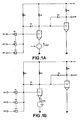
- FIGS. 1 A and 1 B The basic logic circuit is shown in FIGS. 1 A and 1 B, it constitutes an AND gate from which a logic family of a type can be developed which will be called DTTL (Diode Transistor Transistor Logic).
- DTTL Diode Transistor Transistor Logic
- It includes low barrier Schottky diodes D1, D2; ... Dn.
- the cathodes of these diodes constitute the input terminals IN1, IN2 ... INn of the circuit on which are applied input signals A, B ... etc.
- the anodes are connected in common to the base of an NPN type input transistor T1, on the one hand and via an implanted resistor R1 at the supply voltage + V on the other hand.
- the voltage + V is chosen to be equal to 1.7 volts.
- the collector of transistor T1 is connected to the supply voltage + V by an implanted resistor R2 and its emitter is connected to ground by a circuit 1.
- the collector of transistor T1 is connected to the base of an output transistor T2 inverter.
- the emitter of transistor T2 is connected to ground and its collector is connected to the supply voltage + V by an implanted resistor R3.
- the circuit output signal is taken from the output terminal OUT at the collector of transistor T2.
- Two anti-saturation Schottky diodes S1 and S2 with high barrier are disposed between the collector and the base of the transistors T1 and T2.
- this circuit is that the emitter of transistor T1 is connected to ground via circuit 1.
- This circuit can be constituted by a reference voltage source VREF equal to the emitter collector voltage VCE of an NPN transistor, ie 0.3 volts, as shown in FIG. 1 A, or it can be constituted by another logic circuit whose the output signal X is applied to the emitter of transistor T1 as shown in FIG. 1 B.
- the or the corresponding input diodes D1 to Dn are polarized in the forward direction and consequently the transistor T1 is blocked.
- the voltage at the collector of T1 being at the high level, the transistor T2 is conductive and the level of the output signal is low equal to the collector-emitter voltage VCE of the transistor T2.
- the basic circuit of FIG. 1 A therefore performs the AND function of the signals applied to its inputs.
- the circuit of FIG. 2 comprises two input transistors T1-1 and T1-2, provided with anti-saturation Schottky diodes (which is symbolically represented by an S in the diagram of the transistor) and four Schottky diodes of low barrier input D1, D2, D3 and D4.
- the diodes D1 and D2 receive on their cathodes two input signals A and B and have their anodes connected to the base of the transistor T1-1.
- the diodes D3 and D4 receive on their cathodes two input signals C and D and have their anodes connected to the base of the transistor T1-2.
- T1-1 and T1-2 are connected to the supply voltage + V by resistors R1-1 and R1-2 respectively.
- the collectors of T1-1 and T1-2 are connected in common and connected to the supply voltage + V by a resistor R2 and are connected to the base of the inverter output transistor T2, the collector of which is connected to the voltage + V by resistor R3 and the transmitter is connected to ground, as in the circuit of Figure 1 A or 1 B.
- the voltage on the emitters of transistors T1-1 and T1-2 is equal to VREF or that X is at the low level.
- the transistors T1-1 and T1- 1 are blocked and therefore the output transistor T2 is conductive so the output signal is at the low level.
- the transistors T1-1 and T1-2 are conductive and therefore T2 is blocked, therefore the output signal is at the high level.
- T1-1 is blocked and T1-2 is conductive of which T2 is blocked and the output signal is level high.
- T1 ⁇ 2 If one or other of the signals C or D is at the low level and A and B are at the high level T1 ⁇ 2 is blocked and T1-1 is conductive therefore T2 is blocked and the output signal is at the high level .
- the circuit of FIG. 2 performs the function X (AB + CD) or AB + CD.
- the circuit of FIG. 3 is identical to that of FIG. 2 except that the emitters of the two transistors T1-1 and T1-2 are not connected together but receive the output signals X and Y coming from other logic circuits, and consequently it performs the logic function ABX + CDY.
- the circuit of Figure 4 consists of two circuits of Figure 1 B. It includes two input transistors T1-1 and T1-2 and two output transistors T2-1 and T2-2.
- the input transistors T1-1 and T1-2 have their bases connected to the anodes of the input diodes D1, D2 and D3, D4 as in the arrangement of FIG. 3.
- the cathodes of the diodes D1 to D4 receive the signals input A, B, C and D respectively.
- the anodes of diodes D1 and D2 are connected to the supply voltage + V by the resistor R1-1 and the anodes of the diodes D3 and D4 are connected to the supply voltage + V by the resistor R1-2.
- the collector of transistor T1-1 is connected to the base of the first output transistor T2-1 and the collector of transistor T1-2 is connected to the base of the second output transistor T2-2.
- the collectors of the transistors T2-1 and T2-2 are connected in common to the voltage + V by a resistor R3.
- the output OUT is taken to the common collectors of the two output transistors so that the circuit of FIG. 4 performs the logic function (ABX). (CD Y).
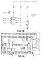
- a microchip comprising cells of the universal type arranged in a conventional manner in rows and columns.
- cells of the universal type arranged in a conventional manner in rows and columns.
- semiconductive elements transistor diodes and resistors which are not connected to each other.
- the cell contains five low barrier Schottky diodes D11 to D15, the cathodes of which constitute the inputs of the logic circuits, seven resistors located R11 to R17 and four transistors T11 to T14 among which T11 is a dual emitter transistor.
- FIG. 5B constitutes a view of the cell in the plane of the first metallization level.
- Their arrangement in the silicon of the chip is such that the connections between the elements are of minimum length, whatever the type of family circuit which will be produced in the cell.
- a grid of 9xl3 possible vias is provided in each cell. The vias are represented by squares in Figure 5B.
- the anodes of the Schottky diodes are identified by the letter A and the cathodes by the letter K.
- the bases, emitters and collectors of the transistors are identified by the letters B, E and C respectively.
- the anti-saturation Schottky diodes, mounted between the collector and the base of the transistors T11 to T14 are not shown.
- each cell is personalized by arranging the appropriate contacts for the pre-diffused elements and wiring at the first metallization level to connect the elements so that the cell performs a logical function with accessible 1/0 inputs-outputs.
- LST Logical Service Terminal
- the wiring between the cells is then carried out at the second and third metallization levels.
- the first step in designing a logic network is to define the first level of metallization.
- a primary LST and several secondary terminals are defined.
- a conventional automatic wiring program defines the interconnections between the primary input / output terminals.
- a secondary terminal is chosen. Only one via among the total number of vias defined for an I / O input / output terminal is used, the others not being made in the final cell thus personalized, the cabling can pass on these unused vias without making contact at the input / output terminals.
- This process gives more freedom for wiring and allows the length, capacity and resistance of the conductors which interconnect the cells to be limited.
- All the logical functions which it is possible to carry out from one or more universal cells are pre-wired to constitute, in an automatic design system assisted by CAD computer, a library of cells which will be available to the designer of logical networks. . These cells can be arranged by automatic positioning and wiring programs to form the network, in accordance with the teachings of European patent 79103921.7 (EP-A-0 011 700).
- FIG. 6A are represented by the shaded parts, the connections necessary to personalize a cell in order to carry out the function of the circuit of FIG. 1B with four inputs.
- FIG. 6B The equivalent diagram is given in FIG. 6B in which the semiconductor elements of the Figure 5B cell have been referenced by the same numbers.
- This cell comprises an input diode D12 receiving the logic signal A and three input transistors constituted by the dual emitter transistor T11 and, the transistor T13 whose collector is connected to the collector of T12, as shown in dotted lines in the figure. 5B.
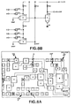
- FIG. 8A are shown the connections necessary for the personalization of a cell carrying out the function AB + CDE, when the emitters of the transistors T13 and T12 are connected to the reference voltage as shown in the diagram equivalent to FIG. 8B.
- the cell of FIG. 8A performs the function X AB + Y CDE.
- the transmitters of T13 and T14 are connected together and receive the output X from another cell, the cell in FIG. 8A performs the function X (AB + CDE).
- FIG. 9A the connections necessary for the personalization of a cell performing the function (A + B + C) D.
- the equivalent diagram is given in FIG. 9B.
- FIG. 10A An example of connections which make it possible to produce a rocker is shown in FIG. 10A.
- the equivalent diagram is given in FIG. 10B.
- circuits By connecting several cells together, circuits, performing complex logic functions, which are often used in logic networks can be created and put in the circuit library available to the designer.
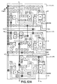
- multiplier / adder circuit produced with three cells, which can enter into the constitution of a multiplier as shown in FIG. 11.
- This multiplier realizes the multiplication of a multiplicand X3 X2 X1 XO and a multiplier Y3 Y2 Y1 YO to supply the product P7 P6 P5 P4 P3 P2 P1 PO as shown in the figure.
- the adder ADD as shown in FIG. 12B comprises a first exclusive OR circuit 10 comprising the transistors T12 and T13 of the cell, the diodes D12 and D15, the output transistor T14 and the resistors R12, R13, R15 and R16.
- This circuit receives as inputs: the factor Pi on the transmitter of T12 and the cathode of the diode D12 and the transfer Ci on the transmitter of T13 and the cathode of D15.
- the anode of diode D12 is connected to the base of T13, and the anode of diode D15 is connected to the base of T12.
- the common collector of the transistors T12 and T13 is connected by the resistor R15 to the voltage + V and is connected at the base to the output transistor T14.
- the transmitter of T14 is connected to ground and its collector is connected to the voltage + V by the resistor R16.
- This circuit constitutes a conventional exclusive OR circuit, therefore the output to the collector of T14 is equal to Pi 0 Ci.
- a second exclusive OR circuit 12 with three inputs is produced in a second cell, and has an arrangement similar to that of circuit 10.
- Transistors T13 and T14 are used, as well as the transistor T11 with double emitter, on which the input signals X and Y are applied.
- the emitter of transistor T13 is connected to the output Pi 0 Ci of cell 10.
- Diode D12 has its cathode connected to the emitter of T13 and its anode connected to the base of T11.
- Diode D15 has its cathode connected to one of the emitters of T11 and its anode connected to the base of T13 and diode D14 has its cathode connected to the other emitter of T11 and its anode connected to the base of T13.
- the output transistor is arranged as in cell 10. So at the output of cell 12, taken at the collector of transistor T14, we get:
- the circuit of cell 14 is identical to that of FIG. 8B and receives Pi, Ci on the one hand, and Pi O Ci, X and Y on the other hand.
- the dotted lines represent the connections at the second metallization level, made in the vertical wiring channels and allows both interconnect the cells and bring them the input signals X, Y, Pi and Ci.
- This type of complex function has been shown, by way of example, but it is obvious that we can consider many others, for example, parity trees made up of exclusive OR circuits can be made using eight cells, a one bit multiplier can be made in three cells, a carry-over prediction circuit for an adder 4 bits can be realized in four cells.
- the universal type cell shown in FIG. 5B in which the circuits of the DTTL family can be made up makes it possible to design logic networks having a power x performance product improved compared to logic networks made up of conventional NON AND cells. Indeed, many reversing stages are eliminated and thus the paths are shortened.
Claims (8)
Priority Applications (4)
| Application Number | Priority Date | Filing Date | Title |
|---|---|---|---|
| EP83430022A EP0130262B1 (de) | 1983-06-30 | 1983-06-30 | Logische Schaltungen, die eine Bildung von sehr dichten logischen Netzwerken gestatten |
| DE8383430022T DE3374638D1 (en) | 1983-06-30 | 1983-06-30 | Logic circuits for creating very dense logic networks |
| JP59098938A JPH073946B2 (ja) | 1983-06-30 | 1984-05-18 | 基本的論理回路 |
| US07/403,062 US4950927A (en) | 1983-06-30 | 1989-09-05 | Logic circuits for forming VLSI logic networks |
Applications Claiming Priority (1)
| Application Number | Priority Date | Filing Date | Title |
|---|---|---|---|
| EP83430022A EP0130262B1 (de) | 1983-06-30 | 1983-06-30 | Logische Schaltungen, die eine Bildung von sehr dichten logischen Netzwerken gestatten |
Publications (2)
| Publication Number | Publication Date |
|---|---|
| EP0130262A1 EP0130262A1 (de) | 1985-01-09 |
| EP0130262B1 true EP0130262B1 (de) | 1987-11-19 |
Family
ID=8191502
Family Applications (1)
| Application Number | Title | Priority Date | Filing Date |
|---|---|---|---|
| EP83430022A Expired EP0130262B1 (de) | 1983-06-30 | 1983-06-30 | Logische Schaltungen, die eine Bildung von sehr dichten logischen Netzwerken gestatten |
Country Status (4)
| Country | Link |
|---|---|
| US (1) | US4950927A (de) |
| EP (1) | EP0130262B1 (de) |
| JP (1) | JPH073946B2 (de) |
| DE (1) | DE3374638D1 (de) |
Families Citing this family (1)
| Publication number | Priority date | Publication date | Assignee | Title |
|---|---|---|---|---|
| US8321938B2 (en) * | 2009-02-12 | 2012-11-27 | Raytheon Bbn Technologies Corp. | Multi-tiered scalable network monitoring |
Family Cites Families (9)
| Publication number | Priority date | Publication date | Assignee | Title |
|---|---|---|---|---|
| FR11700E (fr) * | 1909-03-15 | 1910-04-13 | Carl Grunwald | Four électrique à induction |
| US957007A (en) * | 1909-11-03 | 1910-05-03 | Edwin E Slick | Gas-producer. |
| US3400278A (en) * | 1960-12-28 | 1968-09-03 | Ibm | Non-saturating transistor logic circuit |
| US3751680A (en) * | 1972-03-02 | 1973-08-07 | Signetics Corp | Double-clamped schottky transistor logic gate circuit |
| US3808475A (en) * | 1972-07-10 | 1974-04-30 | Amdahl Corp | Lsi chip construction and method |
| US3836789A (en) * | 1973-06-22 | 1974-09-17 | Ibm | Transistor-transistor logic circuitry and bias circuit |
| UST957007I4 (en) | 1974-03-11 | 1977-04-05 | International Business Machines Corporation | Voltage-mode logic circuitry with improved input/output characteristics |
| GB2035688A (en) * | 1978-11-13 | 1980-06-18 | Hughes Aircraft Co | A multi-function large scale integrated circuit |
| FR2443118A1 (fr) * | 1978-11-30 | 1980-06-27 | Ibm France | Dispositif pour l'alimentation des memoires monolithiques |
-
1983
- 1983-06-30 DE DE8383430022T patent/DE3374638D1/de not_active Expired
- 1983-06-30 EP EP83430022A patent/EP0130262B1/de not_active Expired
-
1984
- 1984-05-18 JP JP59098938A patent/JPH073946B2/ja not_active Expired - Lifetime
-
1989
- 1989-09-05 US US07/403,062 patent/US4950927A/en not_active Expired - Fee Related
Also Published As
| Publication number | Publication date |
|---|---|
| JPS6046619A (ja) | 1985-03-13 |
| JPH073946B2 (ja) | 1995-01-18 |
| EP0130262A1 (de) | 1985-01-09 |
| US4950927A (en) | 1990-08-21 |
| DE3374638D1 (en) | 1987-12-23 |
Similar Documents
| Publication | Publication Date | Title |
|---|---|---|
| US20230299774A1 (en) | Logic drive using standard commodity programmable logic ic chips comprising non-volatile random access memory cells | |
| US6492834B1 (en) | Programmable logic device with highly routable interconnect | |
| US5132571A (en) | Programmable interconnect architecture having interconnects disposed above function modules | |
| US5612633A (en) | Circuit for simultaneously inputting and outputting signals on a single wire | |
| US5777491A (en) | High-performance differential cascode voltage switch with pass gate logic elements | |
| US6002268A (en) | FPGA with conductors segmented by active repeaters | |
| EP0528956B1 (de) | Basiszelle für bicmos-gatterfeld | |
| US4347446A (en) | Emitter coupled logic circuit with active pull-down | |
| US4425516A (en) | Buffer circuit and integrated semiconductor circuit structure formed of bipolar and CMOS transistor elements | |
| US3573488A (en) | Electrical system and lsi standard cells | |
| US4378595A (en) | Synchronous multivalued latch | |
| EP0140584B1 (de) | Integrierte Halbleiter-Schaltungsvorrichtung vom Typ "Master-Slice" | |
| EP0130262B1 (de) | Logische Schaltungen, die eine Bildung von sehr dichten logischen Netzwerken gestatten | |
| US8981814B2 (en) | Permutable switching network with enhanced interconnectivity for multicasting signals | |
| EP0395668A1 (de) | Galliumarsenidlogik-entwurfssystem | |
| US6031982A (en) | Layout design of integrated circuit, especially datapath circuitry, using function cells formed with fixed basic cell and configurable interconnect networks | |
| US5491431A (en) | Logic module core cell for gate arrays | |
| EP0011737B1 (de) | Integrierte Halbleiterschaltung und Verfahren zu deren Herstellung | |
| Chan et al. | Mask-programmable multiple-valued logic gate using resonant tunnelling diodes | |
| Chen et al. | A high-density bipolar logic masterslice for small systems | |
| US6980029B1 (en) | Programmable integrated circuit architecture | |
| Wang et al. | A hierarchical interconnection structure for field-programmable gate arrays | |
| JPS61169015A (ja) | フリツプフロツプ回路 | |
| US4570086A (en) | High speed complementary NOR (NAND) circuit | |
| EP0186720B1 (de) | Vordiffundierte Mehrfunktionstechnik in CMOS-Technik |
Legal Events
| Date | Code | Title | Description |
|---|---|---|---|
| PUAI | Public reference made under article 153(3) epc to a published international application that has entered the european phase |
Free format text: ORIGINAL CODE: 0009012 |
|
| AK | Designated contracting states |
Designated state(s): DE FR GB IT |
|
| 17P | Request for examination filed |
Effective date: 19841123 |
|
| 17Q | First examination report despatched |
Effective date: 19860310 |
|
| GRAA | (expected) grant |
Free format text: ORIGINAL CODE: 0009210 |
|
| AK | Designated contracting states |
Kind code of ref document: B1 Designated state(s): DE FR GB IT |
|
| GBT | Gb: translation of ep patent filed (gb section 77(6)(a)/1977) | ||
| REF | Corresponds to: |
Ref document number: 3374638 Country of ref document: DE Date of ref document: 19871223 |
|
| ITF | It: translation for a ep patent filed |
Owner name: IBM - DR. ARRABITO MICHELANGELO |
|
| PLBE | No opposition filed within time limit |
Free format text: ORIGINAL CODE: 0009261 |
|
| STAA | Information on the status of an ep patent application or granted ep patent |
Free format text: STATUS: NO OPPOSITION FILED WITHIN TIME LIMIT |
|
| 26N | No opposition filed | ||
| ITTA | It: last paid annual fee | ||
| PGFP | Annual fee paid to national office [announced via postgrant information from national office to epo] |
Ref country code: GB Payment date: 19930525 Year of fee payment: 11 |
|
| PGFP | Annual fee paid to national office [announced via postgrant information from national office to epo] |
Ref country code: FR Payment date: 19930601 Year of fee payment: 11 |
|
| PGFP | Annual fee paid to national office [announced via postgrant information from national office to epo] |
Ref country code: DE Payment date: 19930712 Year of fee payment: 11 |
|
| PG25 | Lapsed in a contracting state [announced via postgrant information from national office to epo] |
Ref country code: GB Effective date: 19940630 |
|
| PG25 | Lapsed in a contracting state [announced via postgrant information from national office to epo] |
Ref country code: FR Effective date: 19950228 |
|
| GBPC | Gb: european patent ceased through non-payment of renewal fee |
Effective date: 19940630 |
|
| PG25 | Lapsed in a contracting state [announced via postgrant information from national office to epo] |
Ref country code: DE Effective date: 19950301 |
|
| REG | Reference to a national code |
Ref country code: FR Ref legal event code: ST |