EP0129166A2 - Load cell - Google Patents
Load cell Download PDFInfo
- Publication number
- EP0129166A2 EP0129166A2 EP84106583A EP84106583A EP0129166A2 EP 0129166 A2 EP0129166 A2 EP 0129166A2 EP 84106583 A EP84106583 A EP 84106583A EP 84106583 A EP84106583 A EP 84106583A EP 0129166 A2 EP0129166 A2 EP 0129166A2
- Authority
- EP
- European Patent Office
- Prior art keywords
- strain gauge
- gauge resistors
- load cell
- resistors
- stress
- Prior art date
- Legal status (The legal status is an assumption and is not a legal conclusion. Google has not performed a legal analysis and makes no representation as to the accuracy of the status listed.)
- Granted
Links
Images
Classifications
-
- G—PHYSICS
- G01—MEASURING; TESTING
- G01L—MEASURING FORCE, STRESS, TORQUE, WORK, MECHANICAL POWER, MECHANICAL EFFICIENCY, OR FLUID PRESSURE
- G01L1/00—Measuring force or stress, in general
- G01L1/20—Measuring force or stress, in general by measuring variations in ohmic resistance of solid materials or of electrically-conductive fluids; by making use of electrokinetic cells, i.e. liquid-containing cells wherein an electrical potential is produced or varied upon the application of stress
- G01L1/22—Measuring force or stress, in general by measuring variations in ohmic resistance of solid materials or of electrically-conductive fluids; by making use of electrokinetic cells, i.e. liquid-containing cells wherein an electrical potential is produced or varied upon the application of stress using resistance strain gauges
- G01L1/2287—Measuring force or stress, in general by measuring variations in ohmic resistance of solid materials or of electrically-conductive fluids; by making use of electrokinetic cells, i.e. liquid-containing cells wherein an electrical potential is produced or varied upon the application of stress using resistance strain gauges constructional details of the strain gauges
-
- G—PHYSICS
- G01—MEASURING; TESTING
- G01L—MEASURING FORCE, STRESS, TORQUE, WORK, MECHANICAL POWER, MECHANICAL EFFICIENCY, OR FLUID PRESSURE
- G01L1/00—Measuring force or stress, in general
- G01L1/20—Measuring force or stress, in general by measuring variations in ohmic resistance of solid materials or of electrically-conductive fluids; by making use of electrokinetic cells, i.e. liquid-containing cells wherein an electrical potential is produced or varied upon the application of stress
- G01L1/22—Measuring force or stress, in general by measuring variations in ohmic resistance of solid materials or of electrically-conductive fluids; by making use of electrokinetic cells, i.e. liquid-containing cells wherein an electrical potential is produced or varied upon the application of stress using resistance strain gauges
- G01L1/2206—Special supports with preselected places to mount the resistance strain gauges; Mounting of supports
- G01L1/2243—Special supports with preselected places to mount the resistance strain gauges; Mounting of supports the supports being parallelogram-shaped
-
- G—PHYSICS
- G01—MEASURING; TESTING
- G01L—MEASURING FORCE, STRESS, TORQUE, WORK, MECHANICAL POWER, MECHANICAL EFFICIENCY, OR FLUID PRESSURE
- G01L1/00—Measuring force or stress, in general
- G01L1/20—Measuring force or stress, in general by measuring variations in ohmic resistance of solid materials or of electrically-conductive fluids; by making use of electrokinetic cells, i.e. liquid-containing cells wherein an electrical potential is produced or varied upon the application of stress
- G01L1/22—Measuring force or stress, in general by measuring variations in ohmic resistance of solid materials or of electrically-conductive fluids; by making use of electrokinetic cells, i.e. liquid-containing cells wherein an electrical potential is produced or varied upon the application of stress using resistance strain gauges
- G01L1/225—Measuring circuits therefor
- G01L1/2262—Measuring circuits therefor involving simple electrical bridges
Definitions
- the present invention relates to a load cell having strain gauge resistors and conductive layers formed by a thin film technique.
- a load cell having strain gauge resistors formed through insulation layers on a beam body having a strain generating section and a conductive pattern for forming a bridge circuit by coupling these strain gauge resistors is known.
- these strain gauge resistors and the conductive pattern are formed by depositing, sputtering, or plating.
- the conductive pattern is formed thick.
- resistors while varying in age. In this manner, the resistance values of the strain gauge resistors alter, and bridge balance or span (the output voltage of the load cell) resultantly varies in age, thereby causing the performance of the load cell to be deteriorated.
- the conductive pattern is composed of a conductive layer selectively formed on a resistive layer for forming strain gauge resistors.
- the resistive layer under this conductive layer is contracted or expanded in response to the contraction or expansion of the conductive layer due to the difference of thermal expansion between the resistive layer and the conductive layer.
- a stress generated by this contraction or expansion is transmitted through the insulation layer to the strain gauge resistors, thereby altering the resistance value of the strain gauge resistors to cause the bridge. balance or span to be varied.
- a load cell comprising a beam body having a strain generating section, a plurality of strain gauge resistors formed through an insulation layer on the beam body, a conductive pattern for forming a bridge circuit by coupling these strain gauge resistors, a plurality of compensation resistance sections for compensating the bridge balance and span of the bridge circuit, wherein a section except the section coupled to the strain gauge resistors of the conductive pattern is disposed at a position sufficiently isolated from these strain gauge resistors.
- the aging stress and thermal stress due to this conductive pattern are not substantially transmitted to the strain gauge resistors, but absorbed by the insulation layer so as not to affect the influence thereof to the bridge balance and span.
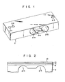
- Fig. 1 shows a beam body 2 used for forming a load cell according an embodiment of the present invention.
- This beam body 2 is obtained, for example, by cutting a stainless steel (SUS 630) or duralumin (A2014, A2024 or A2218).
- the beam body 2 has two through holes 2-1 and 2-2 formed to receive clamping bolts at a stationary end, and a through hole 2-3 formed to receive a supporting clamp (not shown) for supporting a weighing tray at a movable end.
- the beam body 2 has two lateral through holes 2-4 and 2-5 formed to extend laterally, and a coupling hole for coupling the holes 2-4 and 2-5. Those portions of the beam body 2 which correspond to the top portions of the holes 2-4 and 2-5 form a strain generating section.
- an insulation film 4 having, for example, a thickness of 4 pm is first formed of an insulation material formed of an inorganic material such as a Si0 2 or an organic material such as polyimide resin on the beam body 2 as shown in Fig. 2. Then, a resistive layer 6 formed, for example, of a material such as NiCrSi which is used for forming strain gauge resistors and bridge balance correcting resistor and is hardly affected in electric characteristics by the temperature change is formed by sputtering, depositing in a thickness, for example, of 0.1 pm, on the film 4.
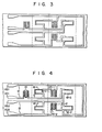
- a laminate of layers 6, 8 and 10 is selectively removed by photoetching, to form a pattern which includes the regions of strain gauge resistors, bridge balance correcting resistor, span temperature compensating resistor, bridge balance temperature compensating resistor, terminal sections and interconnecting sections as shown in Fig. 3.
- the conductive layer 10 in the regions of the strain gauge resistors, bridge balance correcting resistor, span temperature compensating resistor and bridge balance temperature compensating resistor is removed by etching.
- the span temperature compensating resistor 14 and the bridge balance temperature compensating resistors 16-1 and 16-2 are formed of the resistive layer 8 thus exposed, and a power source terminal VE1 and VE2, output terminals VOl and V02, and interconnection sections 12 are formed of the remaining conductive layer 10.
- the resistive layer 8 in the regions of the strain gauge resistors and the bridge balance correcting resistor is subsequently removed by etching, and the resistive layer 6 is exposed.
- Strain gauge resistors 18-1 to 18-4 and bridge balance compensating resistors 20-1 and 20-2 are formed of the resistive layer 6 thus exposed.
- the resistive layer 6 is formed in sufficiently reduced thickness such as, for example, 0.1 pm, and in order to sufficiently reduce the resistance value of the . interconnection section 12, the conductive layer 10 is formed in relatively large thickness of, for example, 2 ⁇ m .
- the span temperature compensating resistor 14, bridge balance temperature compensating resistors 16-1 and 16-2,.and bridge balance correcting resistors 20-1 and 20-2 are disposed at the position where the beam body 2 is not substantially deformed when a load is applied to the load cell. Therefore, when a load is applied to the load cell, an expansion stress is applied to the strain gauge resistors 18-1 and 18-4, and a compression stress is applied to the strain gauge resistors 18-2 and 18-3, but no stress is applied to the other resistors.
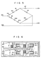
- Fig. 5 shows an equivalent circuit of the load cell thus obtained.
- resistors Rl to R4 respectively correspond to the strain gauge resistors 18-1 to 18-4
- resistors RX1 and RX2 respectively correspond to the bridge balance correcting resistors 20-1 and 30-2
- resistors RY1 and RY2 respectively correspond to the bridge balance temperature compensating resistors 16-1 and 16-2
- a resistor RZ corresponds to the span temperature compensating resistor.
- the interconnection sections 12 are formed separately from these strain gauge resistors 18-1 to 18-4 to surround the strain gauge resistors 18-1 to 18-4, and the influence of the aging stress and thermal stress in these interconnection sections 12 to the resistances of the strain gauge resistors 18-1 to 18-4 is suppressed to the minimum value.
- these interconnection sections 12 include the conductive layer formed to longitudinally extend on both ends of the beam body, and the strain gauge resistors 18-1 to 18-4.are respectively disposed at the equal interval from the corresponding conductive layers.
- Fig. 6 shows a load cell according another embodiment of the present invention.
- This load cell is constructed substantially in the same manner as that shown in Fig. 4 except that having stress generating sections 22-1 to 22-4 formed similarly to the interconnection sections 12 which extend in parallel with each other in the vicinity of strain gauge resistors 18-1 to 18-4.
- Each of the stress generating sections is formed of a laminate of resistive layers and conductive layer formed of the same material as the resistive layers 6 and 8 and conductive layer 10 on an insulation layer 4.
- the dimensions of the stress generating sections 22-1 and 22-2 are empirically determined so that the aging stresses and thermal stress applied by the stress generating sections to the strain gauge resistors 18-1 to 18-4 are proportional to one another, e.g., these stress generating sections 22-1 are formed substantially the same as those of the stress generating sections 22-2, and the distance between the stress generating sections 22-1 and the strain gauge resistor 18-1 is set substantially equal to the distance between the stress generating sections 22-2 and the strain gauge resistor 18-2.
- the sizes of these stress generating sections 22-3 and 22-4 are set equal so that the aging and thermal stresses applied by the stress generating sections 22-3 and 22-4 to the strain gauge resistors 18-3 and 18-4 are proportional to one another.
- the aging and thermal stresses of the stress generating sections 22-1 to 22-4 applied to the strain gauge resistors 18-1 to 18-4 are much larger than those of the interconnection sections 12 applied to the strain gauge resistors 18-1 to 18-4, and the bridge balance can be accordingly maintained substantially constant irrespective of the aging and thermal stresses.
- the bridge balance can also be maintained by respectively setting the dimensions of the stress generating sections 22-1 and 22-4 substantially equal to those of the stress generating sections 22-3 and 22-2, equalizing the stresses of the stress generating sections 22-1 and 22-3 with respect to the strain gauge resistors 18-1 and 18-3, and equalizing the stresses of the stress generating sections 22-2 and 22-4 with respect to the strain gauge resistors 18-2 and 18-4.
Landscapes
- Physics & Mathematics (AREA)
- General Physics & Mathematics (AREA)
- Measurement Of Force In General (AREA)
Abstract
Description
- The present invention relates to a load cell having strain gauge resistors and conductive layers formed by a thin film technique.
- Heretofore, a load cell having strain gauge resistors formed through insulation layers on a beam body having a strain generating section and a conductive pattern for forming a bridge circuit by coupling these strain gauge resistors is known. In the load cell of this type, these strain gauge resistors and the conductive pattern are formed by depositing, sputtering, or plating. In this case, in order to reduce the resistance of the conductive pattern, the conductive pattern is formed thick. Thus, when the conductive pattern is formed to have a strain therein, a stress is produced by this internal strain in the conductive pattern. This stress is transmitted, for example, through an insulation layer to the strain gauge . resistors while varying in age. In this manner, the resistance values of the strain gauge resistors alter, and bridge balance or span (the output voltage of the load cell) resultantly varies in age, thereby causing the performance of the load cell to be deteriorated.
- In the load cell of this type, the conductive pattern is composed of a conductive layer selectively formed on a resistive layer for forming strain gauge resistors. Thus, when this load cell is used at different temperatures, the resistive layer under this conductive layer is contracted or expanded in response to the contraction or expansion of the conductive layer due to the difference of thermal expansion between the resistive layer and the conductive layer. A stress generated by this contraction or expansion is transmitted through the insulation layer to the strain gauge resistors, thereby altering the resistance value of the strain gauge resistors to cause the bridge. balance or span to be varied.
- It is an object of the present invention to provide a load cell in which a bridge balance or span is hardly affected by the influence of temperature change with less aging variation.
- The above object, is achieved by a load cell comprising a beam body having a strain generating section, a plurality of strain gauge resistors formed through an insulation layer on the beam body, a conductive pattern for forming a bridge circuit by coupling these strain gauge resistors, a plurality of compensation resistance sections for compensating the bridge balance and span of the bridge circuit, wherein a section except the section coupled to the strain gauge resistors of the conductive pattern is disposed at a position sufficiently isolated from these strain gauge resistors.
- In the present invention, since most of the conductive pattern is sufficiently isolated from the . strain gauge resistors, the aging stress and thermal stress due to this conductive pattern are not substantially transmitted to the strain gauge resistors, but absorbed by the insulation layer so as not to affect the influence thereof to the bridge balance and span.
- This invention can be more fully understood from the following detailed description when taken in conjunction with the accompanying drawings, in which:
- Fig. 1 is a perspective view of a beam body used for forming a load cell according to an embodiment of the present invention;
- Fig. 2 is a side view showing the structure of a load cell formed with a laminate of insulation, resistive and conductive layers on the beam body;
- Fig. 3 is a plan view showing a pattern formed by selectively etching the laminate of resistive and conductive layers in the load cell structure shown in Fig. 2;
- Fig. 4 is a plan view showing the resistive and conductive layers of the pattern obtained by removing the conductive layer in the section forming the resistors in the pattern obtained in Fig. 3;
- Fig. 5 is an equivalent circuit of the load cell obtained by selectively etching the resistive layer in Fig. 4; and
- Fig. 6 is a plan view showing the section of a load cell according to another embodiment of the present invention.
- Fig. 1 shows a
beam body 2 used for forming a load cell according an embodiment of the present invention. Thisbeam body 2 is obtained, for example, by cutting a stainless steel (SUS 630) or duralumin (A2014, A2024 or A2218). Thebeam body 2 has two through holes 2-1 and 2-2 formed to receive clamping bolts at a stationary end, and a through hole 2-3 formed to receive a supporting clamp (not shown) for supporting a weighing tray at a movable end. Further, thebeam body 2 has two lateral through holes 2-4 and 2-5 formed to extend laterally, and a coupling hole for coupling the holes 2-4 and 2-5. Those portions of thebeam body 2 which correspond to the top portions of the holes 2-4 and 2-5 form a strain generating section. - When a strain sensor is formed on this
beam body 2, an insulation film 4 having, for example, a thickness of 4 pm is first formed of an insulation material formed of an inorganic material such as a Si02 or an organic material such as polyimide resin on thebeam body 2 as shown in Fig. 2. Then, a resistive layer 6 formed, for example, of a material such as NiCrSi which is used for forming strain gauge resistors and bridge balance correcting resistor and is hardly affected in electric characteristics by the temperature change is formed by sputtering, depositing in a thickness, for example, of 0.1 pm, on the film 4. A resistive layer 8 used to form a compensation resistor for compensating the variations of Young's modulus of thebeam body 2 due to the temperature change and of the bridge balance due to the temperature change, is formed on the resistive layer 6. Further, a conductive layer having relatively- large thickness such as 2 µm for forming a conductive pattern is formed on the layer 8. - Then, a laminate of
layers 6, 8 and 10 is selectively removed by photoetching, to form a pattern which includes the regions of strain gauge resistors, bridge balance correcting resistor, span temperature compensating resistor, bridge balance temperature compensating resistor, terminal sections and interconnecting sections as shown in Fig. 3. - Subsequently, as shown by hatched portion in Fig. 4, the
conductive layer 10 in the regions of the strain gauge resistors, bridge balance correcting resistor, span temperature compensating resistor and bridge balance temperature compensating resistor is removed by etching. The spantemperature compensating resistor 14 and the bridge balance temperature compensating resistors 16-1 and 16-2 are formed of the resistive layer 8 thus exposed, and a power source terminal VE1 and VE2, output terminals VOl and V02, andinterconnection sections 12 are formed of the remainingconductive layer 10. Further, the resistive layer 8 in the regions of the strain gauge resistors and the bridge balance correcting resistor is subsequently removed by etching, and the resistive layer 6 is exposed. Strain gauge resistors 18-1 to 18-4 and bridge balance compensating resistors 20-1 and 20-2 are formed of the resistive layer 6 thus exposed. - In order to provide relatively large resistance values in the strain gauge resistors 18-1 to 18-4, the resistive layer 6 is formed in sufficiently reduced thickness such as, for example, 0.1 pm, and in order to sufficiently reduce the resistance value of the .
interconnection section 12, theconductive layer 10 is formed in relatively large thickness of, for example, 2 µm . - Moreover, the span
temperature compensating resistor 14, bridge balance temperature compensating resistors 16-1 and 16-2,.and bridge balance correcting resistors 20-1 and 20-2 are disposed at the position where thebeam body 2 is not substantially deformed when a load is applied to the load cell. Therefore, when a load is applied to the load cell, an expansion stress is applied to the strain gauge resistors 18-1 and 18-4, and a compression stress is applied to the strain gauge resistors 18-2 and 18-3, but no stress is applied to the other resistors. - Fig. 5 shows an equivalent circuit of the load cell thus obtained. In this equivalent circuit, resistors Rl to R4 respectively correspond to the strain gauge resistors 18-1 to 18-4, resistors RX1 and RX2 respectively correspond to the bridge balance correcting resistors 20-1 and 30-2, resistors RY1 and RY2 respectively correspond to the bridge balance temperature compensating resistors 16-1 and 16-2, and a resistor RZ corresponds to the span temperature compensating resistor.
- The condition for maintaining the bridge circuit shown in Fig. 5 in a balanced state is R1/R2 = R3/R4 when the resistors RXl, RX2, RY1 and RY2 are ignored. As shown in Fig. 4, the
interconnection sections 12 are formed separately from these strain gauge resistors 18-1 to 18-4 to surround the strain gauge resistors 18-1 to 18-4, and the influence of the aging stress and thermal stress in theseinterconnection sections 12 to the resistances of the strain gauge resistors 18-1 to 18-4 is suppressed to the minimum value. Further, theseinterconnection sections 12 include the conductive layer formed to longitudinally extend on both ends of the beam body, and the strain gauge resistors 18-1 to 18-4.are respectively disposed at the equal interval from the corresponding conductive layers. Thus, the quantities of variation in the resistances of these strain gauge resistors 18-1 to 18-4 by the aging stress and thermal stress in theinterconnection sections 12 become equal - to each other, so that the balance condition of the bridge circuit is maintained, with the result that aging changes in the bridge balance and span do not occur nor variation occurs in response to the temperature change. - Fig. 6 shows a load cell according another embodiment of the present invention. This load cell is constructed substantially in the same manner as that shown in Fig. 4 except that having stress generating sections 22-1 to 22-4 formed similarly to the
interconnection sections 12 which extend in parallel with each other in the vicinity of strain gauge resistors 18-1 to 18-4. Each of the stress generating sections is formed of a laminate of resistive layers and conductive layer formed of the same material as the resistive layers 6 and 8 andconductive layer 10 on an insulation layer 4. The dimensions of the stress generating sections 22-1 and 22-2 are empirically determined so that the aging stresses and thermal stress applied by the stress generating sections to the strain gauge resistors 18-1 to 18-4 are proportional to one another, e.g., these stress generating sections 22-1 are formed substantially the same as those of the stress generating sections 22-2, and the distance between the stress generating sections 22-1 and the strain gauge resistor 18-1 is set substantially equal to the distance between the stress generating sections 22-2 and the strain gauge resistor 18-2. Similarly, the sizes of these stress generating sections 22-3 and 22-4 are set equal so that the aging and thermal stresses applied by the stress generating sections 22-3 and 22-4 to the strain gauge resistors 18-3 and 18-4 are proportional to one another. - The aging and thermal stresses of the stress generating sections 22-1 to 22-4 applied to the strain gauge resistors 18-1 to 18-4 are much larger than those of the
interconnection sections 12 applied to the strain gauge resistors 18-1 to 18-4, and the bridge balance can be accordingly maintained substantially constant irrespective of the aging and thermal stresses. - The present invention has been described with respect to the embodiments. The present invention is not limited to the particular embodiments. For example, the bridge balance can also be maintained by respectively setting the dimensions of the stress generating sections 22-1 and 22-4 substantially equal to those of the stress generating sections 22-3 and 22-2, equalizing the stresses of the stress generating sections 22-1 and 22-3 with respect to the strain gauge resistors 18-1 and 18-3, and equalizing the stresses of the stress generating sections 22-2 and 22-4 with respect to the strain gauge resistors 18-2 and 18-4.
Claims (6)
Applications Claiming Priority (2)
| Application Number | Priority Date | Filing Date | Title |
|---|---|---|---|
| JP58105497A JPS59230131A (en) | 1983-06-13 | 1983-06-13 | Load cell |
| JP105497/83 | 1983-06-13 |
Publications (3)
| Publication Number | Publication Date |
|---|---|
| EP0129166A2 true EP0129166A2 (en) | 1984-12-27 |
| EP0129166A3 EP0129166A3 (en) | 1987-05-13 |
| EP0129166B1 EP0129166B1 (en) | 1990-09-12 |
Family
ID=14409232
Family Applications (1)
| Application Number | Title | Priority Date | Filing Date |
|---|---|---|---|
| EP84106583A Expired EP0129166B1 (en) | 1983-06-13 | 1984-06-08 | Load cell |
Country Status (4)
| Country | Link |
|---|---|
| US (1) | US4628296A (en) |
| EP (1) | EP0129166B1 (en) |
| JP (1) | JPS59230131A (en) |
| DE (1) | DE3483176D1 (en) |
Cited By (2)
| Publication number | Priority date | Publication date | Assignee | Title |
|---|---|---|---|---|
| DE102016217585B3 (en) * | 2016-09-15 | 2017-08-03 | Schaeffler Technologies AG & Co. KG | Strain gauge and method for making a strain gauge |
| CN114777970A (en) * | 2022-05-23 | 2022-07-22 | 电子科技大学 | Film strain gauge bridge circuit based on flexible circuit board on high-rigidity force measuring knife handle |
Families Citing this family (19)
| Publication number | Priority date | Publication date | Assignee | Title |
|---|---|---|---|---|
| US4777826A (en) * | 1985-06-20 | 1988-10-18 | Rosemount Inc. | Twin film strain gauge system |
| JPS6210628U (en) * | 1985-07-04 | 1987-01-22 | ||
| JPH0711461B2 (en) * | 1986-06-13 | 1995-02-08 | 株式会社日本自動車部品総合研究所 | Pressure detector |
| EP0251563A3 (en) * | 1986-06-17 | 1991-01-09 | Tokyo Electric Co. Ltd. | Photoelectric conversion device |
| JP2666209B2 (en) * | 1986-09-22 | 1997-10-22 | 株式会社テック | Manufacturing method of load cell |
| FR2643148B1 (en) * | 1989-02-15 | 1991-12-06 | Schlumberger Ind Sa | SEMICONDUCTOR-ON-INSULATION PRESSURE SENSOR |
| DE19643868A1 (en) * | 1996-10-30 | 1998-05-07 | Rene Baltus | Load cell with ceramic base and metal face for measuring weight and pressure |
| US6700473B2 (en) * | 2000-02-14 | 2004-03-02 | Kulite Semiconductor Products, Inc. | Pressure transducer employing on-chip resistor compensation |
| JP2001343294A (en) * | 2000-05-31 | 2001-12-14 | Ishida Co Ltd | Load cell and balance |
| US6688185B2 (en) * | 2001-08-20 | 2004-02-10 | Autoliv Asp, Inc. | System and method for microstrain measurement |
| JP2003214962A (en) * | 2002-01-18 | 2003-07-30 | Toyoda Mach Works Ltd | Load sensor |
| US6758098B1 (en) * | 2002-02-20 | 2004-07-06 | The United States Of America As Represented By The Administrator Of The National Aeronautics And Space Administration | Force-measuring clamp |
| US7342185B2 (en) * | 2003-06-10 | 2008-03-11 | The Flintec Group, Ltd. | Compression column load cell with compensation for off center loading errors |
| JP2005233953A (en) * | 2004-02-17 | 2005-09-02 | Robert Bosch Gmbh | Method for manufacturing micromechanical high-pressure sensor and micromechanical pressure sensor |
| US20060185446A1 (en) * | 2005-02-18 | 2006-08-24 | Speckhart Frank H | Printed strain gage for vehicle seats |
| EP2060884A1 (en) * | 2006-09-05 | 2009-05-20 | Ishida Co., Ltd. | Load cell unit, weight checker, electronic weighting instrument, and weighting instrument |
| US8757013B1 (en) * | 2011-07-20 | 2014-06-24 | BG Systems, Inc. | Force transducer with separately mounted calibration resistors |
| US8833176B1 (en) * | 2011-09-04 | 2014-09-16 | Daniel Shapiro | Deadeye for measuring tension in rigging for boats |
| WO2013057689A1 (en) | 2011-10-21 | 2013-04-25 | Ecole Polytechnique Federale De Lausanne (Epfl) | SiC HIGH TEMPERATURE PRESSURE TRANSDUCER |
Citations (4)
| Publication number | Priority date | Publication date | Assignee | Title |
|---|---|---|---|---|
| US4299130A (en) * | 1979-10-22 | 1981-11-10 | Gould Inc. | Thin film strain gage apparatus with unstrained temperature compensation resistances |
| EP0053337A2 (en) * | 1980-11-29 | 1982-06-09 | Tokyo Electric Co., Ltd. | Load cell and method of manufacturing the same |
| DE3042506A1 (en) * | 1980-11-11 | 1982-06-16 | Gould Inc., 60008 Rolling Meadows, Ill. | Temperature compensated thin film strain gauge - having transducer and temperature compensation resistors |
| EP0087665A2 (en) * | 1982-02-18 | 1983-09-07 | Tokyo Electric Co., Ltd. | Strain sensor |
Family Cites Families (9)
| Publication number | Priority date | Publication date | Assignee | Title |
|---|---|---|---|---|
| US2866059A (en) * | 1956-06-01 | 1958-12-23 | Baldwin Lima Hamilton Corp | Slotted type multiple bending beam |
| US3199057A (en) * | 1963-05-03 | 1965-08-03 | Lockheed Aircraft Corp | Load cell transducer |
| US3697918A (en) * | 1971-08-03 | 1972-10-10 | Gen Electric | Silicon diaphragm pressure sensor having improved configuration of integral strain gage elements |
| US4376929A (en) * | 1976-12-27 | 1983-03-15 | Myhre Kjell E | Optimized stress and strain distribution diaphragms |
| US4320664A (en) * | 1980-02-25 | 1982-03-23 | Texas Instruments Incorporated | Thermally compensated silicon pressure sensor |
| US4325048A (en) * | 1980-02-29 | 1982-04-13 | Gould Inc. | Deformable flexure element for strain gage transducer and method of manufacture |
| JPS57196124A (en) * | 1981-05-27 | 1982-12-02 | Toshiba Corp | Load cell |
| JPS57175233A (en) * | 1981-04-21 | 1982-10-28 | Toshiba Corp | Measuring method of residual stress |
| US4462018A (en) * | 1982-11-05 | 1984-07-24 | Gulton Industries, Inc. | Semiconductor strain gauge with integral compensation resistors |
-
1983
- 1983-06-13 JP JP58105497A patent/JPS59230131A/en active Granted
-
1984
- 1984-06-04 US US06/616,964 patent/US4628296A/en not_active Expired - Lifetime
- 1984-06-08 EP EP84106583A patent/EP0129166B1/en not_active Expired
- 1984-06-08 DE DE8484106583T patent/DE3483176D1/en not_active Expired - Lifetime
Patent Citations (4)
| Publication number | Priority date | Publication date | Assignee | Title |
|---|---|---|---|---|
| US4299130A (en) * | 1979-10-22 | 1981-11-10 | Gould Inc. | Thin film strain gage apparatus with unstrained temperature compensation resistances |
| DE3042506A1 (en) * | 1980-11-11 | 1982-06-16 | Gould Inc., 60008 Rolling Meadows, Ill. | Temperature compensated thin film strain gauge - having transducer and temperature compensation resistors |
| EP0053337A2 (en) * | 1980-11-29 | 1982-06-09 | Tokyo Electric Co., Ltd. | Load cell and method of manufacturing the same |
| EP0087665A2 (en) * | 1982-02-18 | 1983-09-07 | Tokyo Electric Co., Ltd. | Strain sensor |
Cited By (3)
| Publication number | Priority date | Publication date | Assignee | Title |
|---|---|---|---|---|
| DE102016217585B3 (en) * | 2016-09-15 | 2017-08-03 | Schaeffler Technologies AG & Co. KG | Strain gauge and method for making a strain gauge |
| US11150073B2 (en) | 2016-09-15 | 2021-10-19 | Schaeffler Technologies AG & Co. KG | Strain gauge having first and second insulation layers and method for producing such a strain gauge |
| CN114777970A (en) * | 2022-05-23 | 2022-07-22 | 电子科技大学 | Film strain gauge bridge circuit based on flexible circuit board on high-rigidity force measuring knife handle |
Also Published As
| Publication number | Publication date |
|---|---|
| JPS59230131A (en) | 1984-12-24 |
| EP0129166A3 (en) | 1987-05-13 |
| JPH0565807B2 (en) | 1993-09-20 |
| US4628296A (en) | 1986-12-09 |
| EP0129166B1 (en) | 1990-09-12 |
| DE3483176D1 (en) | 1990-10-18 |
Similar Documents
| Publication | Publication Date | Title |
|---|---|---|
| EP0129166A2 (en) | Load cell | |
| US4747456A (en) | Load cell and temperature correction of the same | |
| US4432247A (en) | Load cell having thin film strain gauges | |
| US4329878A (en) | Bridge circuit formed of two or more resistance strain gauges | |
| EP0702220B2 (en) | Load cell and weighing apparatus using the same | |
| US4267724A (en) | Strain-gage transducer bridge gages with integral calibration resistors | |
| US9709452B2 (en) | Systems and methods for compensating a sensor | |
| US3290928A (en) | Temperature compensated strain gage and circuit | |
| US4748858A (en) | Strain gage transducer | |
| US5039976A (en) | High-precision, high-stability resistor elements | |
| US5309136A (en) | Electrical circuit such as a Wheatstone bridge with a resistance-adjusting portion | |
| JPH05248925A (en) | Load cell its manufacturing method, gauge and weighing method | |
| JPS5942402A (en) | Production of strain sensor | |
| US10215651B2 (en) | Trimmable links for selectively setting transducer impedance | |
| JPH033882B2 (en) | ||
| GB2142776A (en) | Strain sensor | |
| RU2807002C1 (en) | Strain gauge force sensor | |
| US4365520A (en) | Strain gage transducers | |
| JP2717812B2 (en) | Load cell | |
| JP2554881B2 (en) | Load cell | |
| JPS6225977B2 (en) | ||
| JP3802216B2 (en) | Load cell and load cell temperature compensation method | |
| RU2801776C1 (en) | Strain-resistive sensors signal simulators unit | |
| KR860000048B1 (en) | Load sell and its manufacturing process | |
| JPH11201837A (en) | Load cell and method for compensating temperature of load cell |
Legal Events
| Date | Code | Title | Description |
|---|---|---|---|
| PUAI | Public reference made under article 153(3) epc to a published international application that has entered the european phase |
Free format text: ORIGINAL CODE: 0009012 |
|
| AK | Designated contracting states |
Designated state(s): DE GB |
|
| PUAL | Search report despatched |
Free format text: ORIGINAL CODE: 0009013 |
|
| AK | Designated contracting states |
Kind code of ref document: A3 Designated state(s): DE GB |
|
| 17P | Request for examination filed |
Effective date: 19870902 |
|
| 17Q | First examination report despatched |
Effective date: 19880811 |
|
| GRAA | (expected) grant |
Free format text: ORIGINAL CODE: 0009210 |
|
| AK | Designated contracting states |
Kind code of ref document: B1 Designated state(s): DE GB |
|
| REF | Corresponds to: |
Ref document number: 3483176 Country of ref document: DE Date of ref document: 19901018 |
|
| PLBE | No opposition filed within time limit |
Free format text: ORIGINAL CODE: 0009261 |
|
| STAA | Information on the status of an ep patent application or granted ep patent |
Free format text: STATUS: NO OPPOSITION FILED WITHIN TIME LIMIT |
|
| 26N | No opposition filed | ||
| PGFP | Annual fee paid to national office [announced via postgrant information from national office to epo] |
Ref country code: DE Payment date: 20010605 Year of fee payment: 18 |
|
| PGFP | Annual fee paid to national office [announced via postgrant information from national office to epo] |
Ref country code: GB Payment date: 20010606 Year of fee payment: 18 |
|
| REG | Reference to a national code |
Ref country code: GB Ref legal event code: IF02 |
|
| PG25 | Lapsed in a contracting state [announced via postgrant information from national office to epo] |
Ref country code: GB Free format text: LAPSE BECAUSE OF NON-PAYMENT OF DUE FEES Effective date: 20020608 |
|
| PG25 | Lapsed in a contracting state [announced via postgrant information from national office to epo] |
Ref country code: DE Free format text: LAPSE BECAUSE OF NON-PAYMENT OF DUE FEES Effective date: 20030101 |
|
| GBPC | Gb: european patent ceased through non-payment of renewal fee |
Effective date: 20020608 |