EP0127205A2 - Ignition circuit - Google Patents
Ignition circuit Download PDFInfo
- Publication number
- EP0127205A2 EP0127205A2 EP84200410A EP84200410A EP0127205A2 EP 0127205 A2 EP0127205 A2 EP 0127205A2 EP 84200410 A EP84200410 A EP 84200410A EP 84200410 A EP84200410 A EP 84200410A EP 0127205 A2 EP0127205 A2 EP 0127205A2
- Authority
- EP
- European Patent Office
- Prior art keywords
- ignition
- current
- ignition circuit
- flop
- circuit
- Prior art date
- Legal status (The legal status is an assumption and is not a legal conclusion. Google has not performed a legal analysis and makes no representation as to the accuracy of the status listed.)
- Granted
Links
Images


Classifications
-
- F—MECHANICAL ENGINEERING; LIGHTING; HEATING; WEAPONS; BLASTING
- F02—COMBUSTION ENGINES; HOT-GAS OR COMBUSTION-PRODUCT ENGINE PLANTS
- F02P—IGNITION, OTHER THAN COMPRESSION IGNITION, FOR INTERNAL-COMBUSTION ENGINES; TESTING OF IGNITION TIMING IN COMPRESSION-IGNITION ENGINES
- F02P3/00—Other installations
- F02P3/02—Other installations having inductive energy storage, e.g. arrangements of induction coils
- F02P3/04—Layout of circuits
- F02P3/055—Layout of circuits with protective means to prevent damage to the circuit, e.g. semiconductor devices or the ignition coil
- F02P3/0552—Opening or closing the primary coil circuit with semiconductor devices
-
- F—MECHANICAL ENGINEERING; LIGHTING; HEATING; WEAPONS; BLASTING
- F02—COMBUSTION ENGINES; HOT-GAS OR COMBUSTION-PRODUCT ENGINE PLANTS
- F02P—IGNITION, OTHER THAN COMPRESSION IGNITION, FOR INTERNAL-COMBUSTION ENGINES; TESTING OF IGNITION TIMING IN COMPRESSION-IGNITION ENGINES
- F02P3/00—Other installations
- F02P3/02—Other installations having inductive energy storage, e.g. arrangements of induction coils
- F02P3/04—Layout of circuits
- F02P3/045—Layout of circuits for control of the dwell or anti dwell time
- F02P3/0453—Opening or closing the primary coil circuit with semiconductor devices
Abstract
Description
- This invention relates to an ignition circuit suitable for use in an automotive ignition system having a distributor which is provided with a magnetic sensor.
- Automotive ignition circuits utilising magnetic sensors are known. The magnetic sensor replaces the contact breaker set within the distributor and provides a periodic waveform output.
- The periodic waveform is compared with a reference level and the result of this comparison is used to control both the dwell period i.e. the time during which current flows in the ignition coil and the spark, when the coil current is switched off.
- The dwell time and the spark are defined by the single reference level and this results in this known circuit having disadvantages. Timing errors arise and result in sparks coming too early at low engine speed. Also since the dwell time cannot be regulated over the full speed range the known circuit uses more power than is desirable.
- This invention seeks to provide an automatic ignition circuit suitable for use with a magnetic sensor and in which the above mentioned disadvantages are mitigated.
- According to the present invention there is provided an automotive ignition circuit for controlling the supply of current to an ignition coil and suitable for use in an ignition system in which a distributor is provided with a magnetic sensor, the circuit comprising a first comparator for comparing the amplitude of a periodic signal fed from the magnetic sensor with a first reference potential level and for providing a first output signal indicative of the amplitude of the periodic signal crossing the first reference potential level, a second comparator for comparing the amplitude of the periodic signal with a second reference potential level and for providing a second output signal indicative of the amplitude of the periodic signal crossing the second reference potential level and means for enabling and disabling the supply of current to the ignition coil in response to the first and second output signals respectively.
- In an embodiment of the invention the means for enabling and disabling the supply of current to the ignition coil includes a set-reset flip-flop arranged to be set in response to the said first output signal and reset in response to the said second output signal.
- Differentiating means may be provided between the set-reset flip-flop and the first and second comparators for differentiating the first and second output signals.
- Means may be provided for preventing a change of state of the flip-flop for a predetermined period following the setting and resetting in response to the first and second output signals respectively.
- The means for preventing the change of state of the set-reset flip-flip may comprise gating means positioned between the differentiating means and the set-reset flip-flop, the gating means being blocked for the said predetermined period following the setting and resetting of the flip-flop.
- The gating means may be blocked by an output signal fed from a monostable, triggered in response to the setting and resetting of the flip-flop.
- Means may be provided for maintaining the flip-flop in a reset condition during periods when no periodic signal is provided by the magnetic sensor.
- Means may be provided for adjusting the effective value of the first reference potential level in order to control the point in time during a cycle of the periodic signal at which the supply of current to the ignition coil is enabled.
- The means for adjusting the effective value of the first reference potential may conveniently comprise means for adding a control potential to the periodic signal.
- The control potential may be derived from charge storage means arranged to be charged during a first portion of each cycle of the periodic signal and discharged during a second portion.
- The charge storage means may be charged in response to the periodic signal crossing the second reference potential level in a first predetermined direction and may be discharged in response to the current in the ignition coil attaining a predetermined value, preferably a limiting value.
- Means responsive to distributor speed and/or ignition circuit supply potential may be provided for periodically charging the charge storage means to a reference potential during periods when the distributor speed and/or the supply potential fall below predetermined values.
- The means for enabling and disabling the supply of current to the ignition coil may include one or more output transistors and means may be provided for protecting the said one or more output transistors against potentials greater than a predetermined value.
- An exemplary embodiment of the invention will now be described with reference to the drawings in which:
- Figure 1 is a schematic block diagram of an automotive ignition circuit in accordance with the present invention; and
- Figures 2 - 5 are explanatory waveform diagrams illustrating the operation of the ignition circuit of Figure 1.
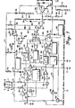
- Referring now to Figure 1 the ignition circuit shown therein is particularly suitable for production on an integrated circuit chip illustrated by a
dashed line box 1, those elements lying within thebox 1 being located on the chip. The circuit operates from a supplypotential line 2 which is coupled to an automotive battery via an ignition switch (not shown). - A
magnetic sensor 3 which replaces the contact breaker set in the automotive distributor hasoutput terminals resistors 6 and 7 to input pins 8 and 9 of thechip 1. A further resistor 10 is coupled between the pins 8 and 9, theresistors 6, 7 and 10 being provided in order to adapt the amplitude of the signal provided by themagnetic sensor 3 to theintegrated circuit chip 1. - The pin 9 is coupled via a
resistor 11 to apositive input 12 of afirst comparator 13 and also to apositive input 14 of asecond comparator 15. - A second and
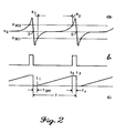
negative input terminal 16 of thecomparator 13 receives a reference potential fromvoltage sources 17 of vaiues Y1 and V4 coupled between theterminal 16 and ground. A second andnegative input terminal 18 of thecomparator 15 also receives a reference potential of value V2 from one terminal of avoltage source 19, a second terminal of which is coupled through a resistor 20 to the pin 8. - Referring also now to Figure 2, when the cam of the distributor is rotating a cyclic waveform as shown in line A of Figure 2 will be developed between the
terminals magnetic sensor 3. In order to control the dwell time, that is the time during which current flows through the ignition coil, a feedback voltage Yc derived in a manner to be described is applied to aterminal 21 and is added to the cyclic waveform derived from themagnetic sensor 3 so that a new cyclic signal Vscis applied to theterminal 12 of thecomparator 13 and is compared with the reference potential provided by thesources 17 at thenegative input 16 of thecomparator 13. - The
comparator 13 provides a rectangular output waveform having a transition each time the cyclic waveform applied to thepositive terminal 12 of the comparator crosses the reference potential applied to thenegative terminal 16. This output waveform of thecomparator 13 is differentiated by adifferentiator 22 which provides an output pulse on each rising edge of the waveform output of thecomparator 13 indicative of the cyclic waveform crossing the reference potential in a first predetermined direction. The differentiated output pulse provided by thedifferentiator 22 is fed to one input of anAND gate 23 whose ouput is connected to aset input 24 of a set-reset flip-flop 25. - The flip-flop 25 has an output 26 connected to a
base 27 of onetransistor 28 of a pair of Darlington connectedoutput transistors transistor 29 having anemitter 30 which is connected to anoutput pin 31 of the ignition circuit. Thetransistors collectors collector 32 of thetransistor 28 being connected to a pin 34 of the integrated circuit whilst thecollector 33 of thetransistor 29 is connected to a pin 35. The pins 34 and 35 are in operation coupled to thesupply potential 2 viaload resistors 36 and 37 respectively. Theoutput pin 31 is coupled to aswitch 38 for switching current flow through theignition coil 39. Thecurrent switch 38 also consists of two Darlington connectedtransistors transistor 41 having itscollector electrode 42 connected to one terminal of the ignition coil 39 a second terminal which is coupled to thesupply potential 2, while emitter electrode 43 of thetransistor 41 is connected to one terminal of aresistor 44 whose other terminal is connected to ground reference potential. - Current through the
ignition coil 39 is turned off by means of thecomparator 15 which compares the cyclic signal provided by themagnetic sensor 3 and appearing between the pins 8 and 9 differentially with the reference potential provided by thesource 19. Thecomparator 15 also provides a rectangular output waveform having a transition edge each time the cyclic waveform crosses the value of the reference potential. - The output waveform of the
comparator 15 is differentiated in adifferentiator 45 which provides an output pulse for each negative going edge of the rectangular waveform indicative of the cyclic waveform falling below the value of the reference potential. Each output pulse provided by thedifferentiator 45 is connected to one input of anAND gate 46 whose output is fed via anOR gate 47 to thereset input 48 of the flip-flop 25. Each pulse at thereset input 48 of the flip-flop 25 is operative to reset the flip-flop and to turn off thetransistors transistors ignition coil 39 thereby producing an ignition spark. - In order to protect the ignition circuit against noise the set and reset
inputs OR gate 49 whose output triggers amonostable multivibrator 50 which in turn has anoutput 51 connected to asecond input 52 of theAND gate 23 and to asecond input 53 of theAND gate 46. Each time the flip-flop 25 changes state the monostable 50 is triggered and provides an output pulse which blocks each of theAND gates - The ignition circuit of the invention as shown in Figure 1 provides accurate ignition timing at different speeds with relatively low power consumption by regulation of the dwell time in accordance with the engine speed. The dwell time is sought to be controlled in such a manner that the time period Tr during which current through the
ignition coil 39 has reached a limiting value is kept at a constant proportion, typically 8% of the period T of the cyclic waveform provided by themagnetic sensor 3. - The potential Vc applied to the
terminal 21 and added to the signal provided by thesensor 3 is dependent upon engine speed and the effect of this added engine speed dependent potential is effectively to vary the reference potential level for thecomparator 13 in dependence upon engine speed. In waveform A as shown in Figure 2 the line V2 represents the fixed value of the reference potential for thecomparator 15 provided by thesource 19, the line Vsc1 represents the effective value of the reference potential of thecomparator 13 for high engine speed, whilst the line Vsc2 represents the effective value of the reference potential for thecomparator 13 at low engine speed. - As can be seen the effective value of the reference potential for the
comparator 13 moves up and down the waveform provided by themagnetic sensor 3 as the engine speed decreases and increases. The range of on-timing, that is the range of variation in time at which current through theignition coil 39 is switched on by the output from thecomparator 13, is defined by the lines of R1 and R2. - At low engine speed the sensor waveform crosses the low speed reference level Vsc2 at one range extremity R2 whilst at high speed the waveform crosses the high speed reference level Vsc1 at the range extremity R1. Coil current is turned off at each downward crossing D by the sensor waveform of the reference potential V2.
- Line B of Figure 2 illustrates current through the ignition coil at low speed whilst the waveform at line C illustrates current through the coil at high speed. At time t1 current begins to flow through the ignition coil, at time t2 current reaches its limiting value and at time t3 current ceases to flow. The timescales of the waveforms B, and C are of course different but the figures clearly illustrate that the current limiting time Tr remains a substantially constant proportion of the period T of the sensor waveform.
- Referring once again to Figure 1 a potential divider formed by series connected
resistors transistor 41 and ground. The junction between theresistors resistor 56 to anegative input 57 of an operational amplifier 58 apositive input 59 of which receives a reference potential of value Y3 from a bandgap reference circuit 60. Theoperational amplifier 58 has afirst output 61 which is operative to turn on acurrent generator 62. Thecurrent source 62 is connected to apin 63 of theintegrated circuit 1 and is operative to discharge a capacitor 64 which is connected externally of theintegrated circuit 1 between thepin 63 and ground. A secondcurrent source 65 is connected in parallel with thecurrent source 62 between thepin 63 and ground and is operative to charge the capacitor 64. Thecurrent source 65 is turned on by a leading edge of the rectangular waveform fed via aconnection 66 from the output of thecomparator 15. - The instantaneous potential appearing on the capacitor 64 is applied via a
voltage follower 67 to the terminal 21 where it is added to the waveform provided by themagnetic sensor 3 and is operative to change effectively the reference level of thecomparator 13 and hence to control the dwell time. Typically thecurrent source 62 which discharges the capacitor 64 generates a current which is approximately six times that generated by thecurrent source 65 which charges the capacitor 64. - In operation the
current source 65 is firstly turned on by means of the output waveform fed from thecomparator 15 and thiscurrent source 65 charges the capacitor 64. A current flowing through theignition coil 39 builds up and consequently the potential applied to theinput terminal 57 of theoperational amplifier 58, which is representative of the value amplitude of the current flowing through the ignition coil also increases. The reference potential applied to theinput terminal 59 of theoperational amplifier 58 is set at a value representative of the coil reaching its maximum, i.e. limiting, value and when this limiting value is reached theoperational amplifer 61 will provide an output signal at itsoutput 61 which switches on thecurrent source 62 which commences to discharge the capacitor 64. - The
operational amplifier 58 is also utilized to regulate the coil current by providing asecond output 68 connected to thebase electrode 27 of thetransistor 28. In this way current through theoutput transistors ignition coil 39, are regulated. - A problem can arise at low speed and low supply voltage. Under these conditions it is possible that the current flowing through the
ignition coil 39 may never reach its limiting value. Consequently in each cycle of the waveform provided by themagnetic sensor 3, the output fed from thecomparator 15 will turn on thecurrent source 65 to charge the capacitor 64 but because the coil current never limits, thecurrent source 62 will never be turned on. The effect of this is illustrated in Figure 3 to which reference will now be made. - In Figure 3 and considering firstly Figure 3A the level of the potential V4 is indicated, together with the level V4 + V1 representing the actual potential applied to the
input 16 of thecomparator 13 and derived from the voltage sources 17. The waveform Ym is the sensor waveform applied between theinput terminals comparator 15 whilst the waveform Vsc is the waveform applied to thepositive input terminal 12 of thecomparator 13. Figure 38 shows the waveform output provided by thecomparator 15 whilst the waveform shown in Figure 3C illustrates the increasing potential on the capacitor 64. Ignition coil current is illustrated in Figure 3D and the line IL indicates the limiting value of the coil current. As can be seen in Figure 3A the effect of the steadily increasing charge on the capacitor 64 is to cause the overall level of the waveform Vsc to rise until it no longer crosses the level Von applied to thenegative input terminal 16 of thecomparator 13. The points P1, P2 and P3 at which the waveform Vsc crosses the level Von represent the turning on of the coil current caused by an output of thecomparator 13 and as can be seen the point P3 will be the last turn on of this coil current. Thereafter the coil current will not be turned on and the ignition circuit will cease to function properly. - This problem is overcome by connecting the
pin 63 to thepotential source 17 through aswitch 69 which is normally open. The switch is closed in response to an output pulse provided by a speed detector 70 which provides output pulses in response to being triggered at a triggeringinput 71 by means of the output waveform fed from thecomparator 15. The speed detector 70 provides output pulses following triggering after either a delay time T1 or T2. The delay time T1 or T2 is chosen in dependence upon supply voltage as follows. Aninput pin 72 of thecircuit 1 is coupled to thesupply potential 2 through aresistor 73. AZener diode 74 is connected between thepin 72 and ground potential. Avoltage detector 75 is also connected to thepin 72 and detects whether or not theZener diode 74 is limiting, which limiting takes place at normal supply voltage. - The
voltage detector 75 controls current supplied by a current source 76 connected to acontrol input 79 of the speed detector 70. Thecontrol input 79 is also connected to apin 78 of theintegrated circuit chip 1. Anexternal capacitor 77 is coupled between thepin 78 and ground. - The current source 76 and the
capacitor 77 are the time determining elements of the speed detector 70. At low supply voltages thevoltage detector 75 controls the current supplied by the source 76 to a first relatively high value so that the speed detector operates on delay time T1 which is dimensioned such that output pulses provided by the speed detector 70 disappear at a frequency at which the output waveform provided by themagnetic sensor 3 is sufficiently large that the critical situation illustrated in Figure 3 does not occur. At speeds higher than this critical frequency the speed detector 70 will be retriggered before an ouput pulse is provided so that no output pulses will occur. - Where speed falls below this critical value so that periodically an output pulse is provided by the speed detector 70 this pulse operates to close the
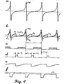
switch 69 thereby connecting the capacitor 64 to thepotential source 17. This results in the capacitor 64 being charged to the reference level of thepotential source 17 each time that an ouput pulse is provided by the speed detector 70. The effect of periodically charging the capacitor 64 to the reference potential of thesource 17 will now be described with reference to Figure 4. - In Figure 4, Figure 4A illustrates the magnetic sensor waveform Vm, Figure 4C illustrates the output of the
comparator 15 Figure 4D shows the output pulses provided by the speed detector 70, the period Tc representing the period of the output pulses of the speed detector during which theswitch 69 is closed. Figure 4E shows the potential on the capacitor 64 whilst Figure 4F illustrates the current through theignition coil 39. This current through the coil as shown in Figure 4F once again can be seen not to rise to the limiting value IL. During the period Tc, during which theswitch 69 is closed due to the speed detector 70 not having been reset for a period Tl, the potential on the capacitor 64 is held at the potential Von of thesource 17. The effect of this on the waveform applied to thepositive input terminal 12 of thecomparator 13 is illustrated in Figure 4B. The waveform Vsc can be seen to be stepped down in level at points Pc which correspond to the closing of theswitch 69 so that the waveform does not continue to rise above the levels of the reference potentials V4 + V4 and V1 but continues to cycle about those levels. The ignition circuit keeps its high sensitivity and normal operation at low supply voltage and speed. - At normal supply voltage the speed detector 70 is switched to a much longer time constant T2 and as will now be seen this longer time constant enables the speed detector to detect very low speeds e.g. cranking speeds to ensure that the ignition circuit can follow acceleration and deceleration at such low speed. When the
voltage detector 75 detects limiting of theZener diode 74 the current supplied by the current source 76 is switched to a much lower value so that the delay time of the speed detector 70 adopts the much longer time constant T2. Typically the speed detector 70 will provide outputs at delay T1 at distributor speeds of 430 revolutions per minute whilst the delay time T2 becomes operative at distributor speeds of 60 r.p.m. - Operation of the ignition circuit with the speed detector 70 at very low speed is illustrated in Figure 5 to which reference will now be made.
- In Figure 5, Figure 5A illustrates the sensor waveform Vm together with the waveform Vsc applied to the
positive input 12 of thecomparator 13. The levels L1, L2 and L3 represent the spark level set by the potential V2, the ON level for thecurrent source 65 and the on level for thecurrent source 62 respectively. Waveform 5B shows the output of thecomparator 15, Figure 5D shows the potential on the capacitor 64, whilst the waveform 5E illustrates the current through theignition coil 39. - A problem at very low speed such as cranking speed is that the amplitude of the sensor waveform Ym becomes so small that the
comparator 15 switches thecurrent source 65 on for such a short period during each cycle that the capacitor 64 remains substantially totally discharged. As can be seen in Figure 5A it is possible that the sensor waveform may not cross the reference level V4 + Y1. In Figure 5C the speed detector 70 can be seen to provide an output pulse which commences at a delay time T2 after triggering and continues until retriggered by another output from thecomparator 15. In Figure 5D the capacitor 64 can be seen to be charging for a short period following the end of the period Tc. In this way the voltage level VSC can rise until it becomes equal to V4 + V1 so thatcomparator 13 can switch the coil current on. As soon as the current is at its limiting value, capacitor 64 is discharged again bycurrent source 62. The capacitor 64 can be seen to be prevented from remaining permanently discharged as during each period Tc during which output pulses provded by the speed detector 70 theswitch 69 closes and the capacitor 64 is restored to the reference level V4. The ignition circuit can in this way follow any acceleration or deceleration at very low speed. - The ignition circuit has several protection devices. A
circuit 80 is also triggered by the output signal fed from thecomparator 15. In the absence of an output waveform from thecomparator 15, i.e. when the distributor is not rotating, anoutput 81 is fed from thecircuit 80 through a second input of theOR gate 47 to the reset input of the flip-flop 25 to maintain that flip-flop in a reset condition and thereby prevent current flowing through theignition coil 39. The ignition coil is therefore prevented from being burnt out whilst the distributor is not rotating. A power-onreset circuit 82 is also provided and this circuit has anoutput 83 also coupled to a third input of theOR gate 47. The power-onreset circuit 82 senses the initial application of thesupply potential 2 and provides an output pulse to re-set the flip-flop 25 until such time as a sensor waveform is provided by themagnetic sensor 3 during the starting of the engine. - An over voltage protection circuit is provided for the Darlington connected
transistors resistors supply potential 2 and ground. The junction of these resistors is coupled to pin 86 of thechip 1. AZener diode 87 is coupled between thepin 86 and abase electrode 88 of a pair of Darlington connectedtransistors transistor 90 of the Darlington connected pair is coupled to a further pin 91 of the chip, which pin is connected through aresistor 92 to the pin 35 to which thecollector electrode 33 of thetransistor 29 is connected. When the potential at thepin 86 exceeds the breakdown voltage of theZener diode 87 the pin 91 which is coupled to the collector electrode of thetransistor 90 is pulled down the clamps the potential at the pin 35 to a safe voltage at which theoutput transistor resistors transistors switch 38 are protected by means of afurther Zener diode 93 mounted on the integrated circuit chip and connected between apin 94 and theoutput pin 31 of the chip. Two series connectedresistors collector electrode 42 of thetransistor 41 and ground potential and thepin 94 of the chip is coupled to the junction of theresistors - The invention has been described by way of example only and modifications may be made without departing from the scope of the invention.
Claims (15)
Applications Claiming Priority (2)
| Application Number | Priority Date | Filing Date | Title |
|---|---|---|---|
| GB8308405 | 1983-03-26 | ||
| GB08308405A GB2138495B (en) | 1983-03-26 | 1983-03-26 | Automotive ignition systems |
Publications (3)
| Publication Number | Publication Date |
|---|---|
| EP0127205A2 true EP0127205A2 (en) | 1984-12-05 |
| EP0127205A3 EP0127205A3 (en) | 1985-04-10 |
| EP0127205B1 EP0127205B1 (en) | 1989-01-04 |
Family
ID=10540308
Family Applications (1)
| Application Number | Title | Priority Date | Filing Date |
|---|---|---|---|
| EP19840200410 Expired EP0127205B1 (en) | 1983-03-26 | 1984-03-22 | Ignition circuit |
Country Status (4)
| Country | Link |
|---|---|
| EP (1) | EP0127205B1 (en) |
| DE (1) | DE3475934D1 (en) |
| GB (1) | GB2138495B (en) |
| SG (1) | SG41189G (en) |
Families Citing this family (4)
| Publication number | Priority date | Publication date | Assignee | Title |
|---|---|---|---|---|
| US4894602A (en) * | 1988-06-02 | 1990-01-16 | Brunswick Corporation | Overvoltage protection system for marine ignition and regulator circuitry |
| DE3926888A1 (en) * | 1989-08-16 | 1991-02-21 | Bosch Gmbh Robert | DARLINGTON TRANSISTOR CIRCUIT |
| FR2730277B1 (en) * | 1995-02-03 | 1997-03-14 | Thomson Csf | REAL TIME INTEGRAL ELECTRONIC IGNITION DEVICE |
| US10502176B2 (en) * | 2012-10-15 | 2019-12-10 | Ford Global Technologies, Llc | System and method for delivering spark to an engine |
Citations (3)
| Publication number | Priority date | Publication date | Assignee | Title |
|---|---|---|---|---|
| US3882840A (en) * | 1972-04-06 | 1975-05-13 | Fairchild Camera Instr Co | Automotive ignition control |
| US3938490A (en) * | 1974-07-15 | 1976-02-17 | Fairchild Camera And Instrument Corporation | Internal combustion engine ignition system for generating a constant ignition coil control signal |
| US3991730A (en) * | 1975-01-30 | 1976-11-16 | Chrysler Corporation | Noise immune reset circuit for resetting the integrator of an electronic engine spark timing controller |
Family Cites Families (5)
| Publication number | Priority date | Publication date | Assignee | Title |
|---|---|---|---|---|
| GB1409748A (en) * | 1972-04-06 | 1975-10-15 | Fairchild Camera Instr Co | Ignition control systems |
| DE2549586C3 (en) * | 1975-11-05 | 1979-03-29 | Robert Bosch Gmbh, 7000 Stuttgart | Ignition device for internal combustion engines |
| US4117819A (en) * | 1976-10-26 | 1978-10-03 | Motorola, Inc. | Threshold circuit suitable for use in electronic ignition systems |
| DE2729505C2 (en) * | 1977-06-30 | 1985-05-23 | Robert Bosch Gmbh, 7000 Stuttgart | Ignition device for internal combustion engines |
| DE3043247A1 (en) * | 1980-11-15 | 1982-07-08 | Robert Bosch Gmbh, 7000 Stuttgart | IGNITION DEVICE FOR INTERNAL COMBUSTION ENGINES |
-
1983
- 1983-03-26 GB GB08308405A patent/GB2138495B/en not_active Expired
-
1984
- 1984-03-22 DE DE8484200410T patent/DE3475934D1/en not_active Expired
- 1984-03-22 EP EP19840200410 patent/EP0127205B1/en not_active Expired
-
1989
- 1989-07-10 SG SG41189A patent/SG41189G/en unknown
Patent Citations (3)
| Publication number | Priority date | Publication date | Assignee | Title |
|---|---|---|---|---|
| US3882840A (en) * | 1972-04-06 | 1975-05-13 | Fairchild Camera Instr Co | Automotive ignition control |
| US3938490A (en) * | 1974-07-15 | 1976-02-17 | Fairchild Camera And Instrument Corporation | Internal combustion engine ignition system for generating a constant ignition coil control signal |
| US3991730A (en) * | 1975-01-30 | 1976-11-16 | Chrysler Corporation | Noise immune reset circuit for resetting the integrator of an electronic engine spark timing controller |
Also Published As
| Publication number | Publication date |
|---|---|
| GB8308405D0 (en) | 1983-05-05 |
| EP0127205A3 (en) | 1985-04-10 |
| SG41189G (en) | 1989-12-22 |
| GB2138495A (en) | 1984-10-24 |
| GB2138495B (en) | 1987-02-18 |
| EP0127205B1 (en) | 1989-01-04 |
| DE3475934D1 (en) | 1989-02-09 |
Similar Documents
| Publication | Publication Date | Title |
|---|---|---|
| US6283104B1 (en) | Ignition system for internal combustion engine | |
| US3881458A (en) | Ignition system dependent upon engine speed | |
| US4202304A (en) | Interference protected electronic ignition system for an internal combustion engine | |
| GB1359055A (en) | Ignition systems | |
| GB1287058A (en) | Maximum engine speed limiting ignition system | |
| US5367424A (en) | Circuit for protecting an electronic switch against short circuits | |
| US4167927A (en) | Contactless ignition control system with a dwell time control circuit for an internal combustion engine | |
| US4404940A (en) | Engine speed limiting circuit | |
| EP0343536B1 (en) | Circuit for controlling the power supply of an electrical load, having a device for detecting a short-circuit of the load | |
| US4138977A (en) | Ignition system for internal combustion engine | |
| GB1594276A (en) | Ignition system for internal combustion engines | |
| GB982015A (en) | Improvements in or relating to overspeed controls for internal combustion engines | |
| US4185603A (en) | Supply voltage variation compensated ignition system for an internal combustion engine | |
| US4335692A (en) | Spark ignition timing control system for internal combustion engines | |
| EP0080496A1 (en) | Noise blanker circuit for use with electronic ignition systems or the like | |
| US4237835A (en) | Speed-dependent ignition timing system for internal combustion engines | |
| EP0127205B1 (en) | Ignition circuit | |
| US4446843A (en) | Adaptive dwell ignition system | |
| US4356808A (en) | Low-speed compensated ignition system for an internal combustion engine | |
| US4204508A (en) | Ignition system for internal combustion engine | |
| GB1575254A (en) | Speed limiting apparatus for internal combustion engines | |
| US3970872A (en) | Circuit for generating a trigger blanking voltage for use in analysis of the ignition voltage waveform of an internal combustion engine | |
| EP0077365B1 (en) | Ignition system having variable percentage current limiting | |
| US4448180A (en) | Ignition system for an internal combustion engine | |
| US3853107A (en) | Capacitive discharge ignition system |
Legal Events
| Date | Code | Title | Description |
|---|---|---|---|
| PUAI | Public reference made under article 153(3) epc to a published international application that has entered the european phase |
Free format text: ORIGINAL CODE: 0009012 |
|
| AK | Designated contracting states |
Designated state(s): DE FR IT |
|
| PUAL | Search report despatched |
Free format text: ORIGINAL CODE: 0009013 |
|
| AK | Designated contracting states |
Designated state(s): DE FR IT |
|
| 17P | Request for examination filed |
Effective date: 19851008 |
|
| 17Q | First examination report despatched |
Effective date: 19870625 |
|
| ITF | It: translation for a ep patent filed |
Owner name: BARZANO' E ZANARDO ROMA S.P.A. |
|
| GRAA | (expected) grant |
Free format text: ORIGINAL CODE: 0009210 |
|
| AK | Designated contracting states |
Kind code of ref document: B1 Designated state(s): DE FR IT |
|
| REF | Corresponds to: |
Ref document number: 3475934 Country of ref document: DE Date of ref document: 19890209 |
|
| ET | Fr: translation filed | ||
| PLBE | No opposition filed within time limit |
Free format text: ORIGINAL CODE: 0009261 |
|
| STAA | Information on the status of an ep patent application or granted ep patent |
Free format text: STATUS: NO OPPOSITION FILED WITHIN TIME LIMIT |
|
| 26N | No opposition filed | ||
| PGFP | Annual fee paid to national office [announced via postgrant information from national office to epo] |
Ref country code: FR Payment date: 19900120 Year of fee payment: 7 |
|
| PGFP | Annual fee paid to national office [announced via postgrant information from national office to epo] |
Ref country code: DE Payment date: 19900129 Year of fee payment: 7 |
|
| ITTA | It: last paid annual fee | ||
| PG25 | Lapsed in a contracting state [announced via postgrant information from national office to epo] |
Ref country code: FR Effective date: 19911129 |
|
| PG25 | Lapsed in a contracting state [announced via postgrant information from national office to epo] |
Ref country code: DE Effective date: 19920101 |
|
| REG | Reference to a national code |
Ref country code: FR Ref legal event code: ST |