EP0343536B1 - Circuit for controlling the power supply of an electrical load, having a device for detecting a short-circuit of the load - Google Patents
Circuit for controlling the power supply of an electrical load, having a device for detecting a short-circuit of the load Download PDFInfo
- Publication number
- EP0343536B1 EP0343536B1 EP89109088A EP89109088A EP0343536B1 EP 0343536 B1 EP0343536 B1 EP 0343536B1 EP 89109088 A EP89109088 A EP 89109088A EP 89109088 A EP89109088 A EP 89109088A EP 0343536 B1 EP0343536 B1 EP 0343536B1
- Authority
- EP
- European Patent Office
- Prior art keywords
- circuit
- load
- transistor
- voltage
- capacitor
- Prior art date
- Legal status (The legal status is an assumption and is not a legal conclusion. Google has not performed a legal analysis and makes no representation as to the accuracy of the status listed.)
- Expired - Lifetime
Links
- 239000003990 capacitor Substances 0.000 claims description 30
- 230000001939 inductive effect Effects 0.000 claims description 11
- 238000010200 validation analysis Methods 0.000 claims description 9
- 238000001514 detection method Methods 0.000 description 14
- 230000000873 masking effect Effects 0.000 description 6
- 230000004048 modification Effects 0.000 description 6
- 238000012986 modification Methods 0.000 description 6
- 230000009471 action Effects 0.000 description 4
- 238000011161 development Methods 0.000 description 4
- 230000018109 developmental process Effects 0.000 description 4
- 230000007423 decrease Effects 0.000 description 3
- 239000000446 fuel Substances 0.000 description 3
- 238000004519 manufacturing process Methods 0.000 description 3
- 238000012544 monitoring process Methods 0.000 description 3
- 238000004804 winding Methods 0.000 description 3
- 238000005516 engineering process Methods 0.000 description 2
- 239000012530 fluid Substances 0.000 description 2
- 230000006870 function Effects 0.000 description 2
- 230000010354 integration Effects 0.000 description 2
- 230000009467 reduction Effects 0.000 description 2
- 230000004044 response Effects 0.000 description 2
- 230000001960 triggered effect Effects 0.000 description 2
- 230000033228 biological regulation Effects 0.000 description 1
- 239000000110 cooling liquid Substances 0.000 description 1
- 230000002950 deficient Effects 0.000 description 1
- 230000001934 delay Effects 0.000 description 1
- 238000007599 discharging Methods 0.000 description 1
- 230000000694 effects Effects 0.000 description 1
- 238000001914 filtration Methods 0.000 description 1
- 239000007788 liquid Substances 0.000 description 1
- 230000015654 memory Effects 0.000 description 1
- 238000009877 rendering Methods 0.000 description 1
- 230000035945 sensitivity Effects 0.000 description 1
Images

Classifications
-
- H—ELECTRICITY
- H02—GENERATION; CONVERSION OR DISTRIBUTION OF ELECTRIC POWER
- H02H—EMERGENCY PROTECTIVE CIRCUIT ARRANGEMENTS
- H02H1/00—Details of emergency protective circuit arrangements
- H02H1/04—Arrangements for preventing response to transient abnormal conditions, e.g. to lightning or to short duration over voltage or oscillations; Damping the influence of DC component by short circuits in AC networks
-
- H—ELECTRICITY
- H02—GENERATION; CONVERSION OR DISTRIBUTION OF ELECTRIC POWER
- H02H—EMERGENCY PROTECTIVE CIRCUIT ARRANGEMENTS
- H02H3/00—Emergency protective circuit arrangements for automatic disconnection directly responsive to an undesired change from normal electric working condition with or without subsequent reconnection ; integrated protection
- H02H3/08—Emergency protective circuit arrangements for automatic disconnection directly responsive to an undesired change from normal electric working condition with or without subsequent reconnection ; integrated protection responsive to excess current
- H02H3/087—Emergency protective circuit arrangements for automatic disconnection directly responsive to an undesired change from normal electric working condition with or without subsequent reconnection ; integrated protection responsive to excess current for DC applications
-
- H—ELECTRICITY
- H03—ELECTRONIC CIRCUITRY
- H03K—PULSE TECHNIQUE
- H03K17/00—Electronic switching or gating, i.e. not by contact-making and –breaking
- H03K17/08—Modifications for protecting switching circuit against overcurrent or overvoltage
- H03K17/082—Modifications for protecting switching circuit against overcurrent or overvoltage by feedback from the output to the control circuit
- H03K17/0826—Modifications for protecting switching circuit against overcurrent or overvoltage by feedback from the output to the control circuit in bipolar transistor switches
-
- Y—GENERAL TAGGING OF NEW TECHNOLOGICAL DEVELOPMENTS; GENERAL TAGGING OF CROSS-SECTIONAL TECHNOLOGIES SPANNING OVER SEVERAL SECTIONS OF THE IPC; TECHNICAL SUBJECTS COVERED BY FORMER USPC CROSS-REFERENCE ART COLLECTIONS [XRACs] AND DIGESTS
- Y10—TECHNICAL SUBJECTS COVERED BY FORMER USPC
- Y10S—TECHNICAL SUBJECTS COVERED BY FORMER USPC CROSS-REFERENCE ART COLLECTIONS [XRACs] AND DIGESTS
- Y10S323/00—Electricity: power supply or regulation systems
- Y10S323/901—Starting circuits
Definitions
- the present invention relates to a circuit for controlling the power supply of an electrical load provided with a device for detecting a short-circuit of the load. More particularly, the invention relates to such a circuit designed for controlling the power supply of an inductive load whose detecting device monitors the possible short-circuiting of the load in order that a corrective action may be triggered in response intended to prevent, for example, damage to the circuit by this short-circuit of the load or defective functioning of a unit fitted with this load.
- actuators comprise such inductive loads.
- winding of a fuel injector or that of an electrovalve varying the pressure of a braking fluid in an anti-locking device for the wheels of a vehicle.
- coil of an inductive primary ignition circuit is furthermore possible to mention the coil of an inductive primary ignition circuit.
- the circuits controlling such inductive loads in a motor vehicle environment are often fitted with diagnostic means enabling the detection, for example, of a disconnection or an accidental short-circuit of the inductive load rendering the latter inoperative, this detection being made for reasons of safety for example.
- diagnostic means comprise electronic circuits which monitor the voltage existing at the terminals of the load in order to detect, for example, the possible appearance of a short-circuit and to trigger alarm actions or appropriate corrective actions.
- the voltage sampled at the terminals of the load must be filtered in order that it may be used, the filtered signal being compared with a reference voltage.
- the means of comparison used trigger the supply of a signal representative of a short-circuited state of the load.
- FIG. 1 of the accompanying drawing shows a circuit for controlling the power supply of an actuator having an inductive load, of the prior art.
- the circuit comprises a power transistor 1 controlled by its base 5 in order to initiate the power supply of an inductive load 2 connected in series with the emitter-collector circuit of the power transistor, between the collector of the latter and ground.
- the power supply voltage +Vbat is supplied by the battery of a motor vehicle.
- a filter 3 for example a low pass capacitive filter, takes the voltage from the terminal which is common to the inductive load 2 and the collector of the transistor 1 in order to filter out the interference from this signal before applying it to an input E of the control unit 4 which is designed to use the signal received from the filter 3.
- the unit 4 also controls the conduction of the power transistor via a terminal S connected to the base of this transistor, through an actuator control sub-circuit 5.
- control unit conventionally comprises a microprocessor
- the delay is obtained by means of a parallel loaded counter initialized by the microprocessor.
- the voltage signal at the terminals of the load could also be filtered by digital means.
- the masking logic necessary for obtaining a digital delay has the disadvantage of being expensive.
- the delay to be generated must in practice be able to reach values in the order of 200 ⁇ s which, for a resolution of 2 ⁇ s, involves the use of a parallel loaded 7-bit counter in order to be programmable, a requirement which additionally demands the presence of a 7-bit register and the associated logic.
- the assembly requires the integration of about 200 MOS transistors per counter resulting in an expensive production.
- Another object of the present invention is to provide such an integrated circuit which is less expensive than that of the digital masking means mentioned above.
- Another object of the present invention is to provide such a device in which the characteristics of the device for detecting a short-circuit of the load are independent of those of the filter used for removing interference from the voltage sampled at the terminals of the load. Such a circuit is thus easily adapted to a modification of this filter.
- a circuit for controlling the power supply of an electrical load having a device for detecting a short-circuit of the load by comparison of a reference voltage with a voltage sampled at the terminals of the load and filtered in a capacitive filter, this circuit being characterized in that it comprises means, actuated by the switching on of the electrical load, for pre-charging the capacitor of the filter in order to initially establish on the output of this capacitor a voltage substantially equal to the reference voltage, the time constant of the charging of the capacitor by these means being low with respect to that which corresponds to the charging of this capacitor by the supply voltage of the load alone.
- These pre-charging means comprise a connecting transistor for connecting the capacitor of the filter to a pre-charging voltage source and a logic sub-circuit for triggering the conduction of the transistor when the load is switched on.
- the comparison of the reference voltage with the voltage sampled at the terminals of the load is performed by a comparator whose inputs are respectively supplied by these voltages.
- the logic sub-circuit then comprises a logic AND gate having two inputs respectively connected to the output of the comparator and to a source of a validation signal of predetermined duration, the output of the AND gate supplying a control pin of the connecting transistor.
- a power transistor 1 controls the electrical power supply of a load 2.
- the transistor 1 can be a transistor of the MOS technology type, or of the bipolar technology type as shown in the drawing in which it takes the form of a PNP type transistor connected by its emitter to the + pole of an electrical power supply source.
- this power supply source is the battery of the vehicle which therefore supplies a voltage + Vbat.
- the load 2 typically an inductive winding in motor vehicle electronics, is then in this case part of an actuator, for example, an electrovalve which varies the pressure or the flow rate of a fluid. Such an electrovalve can thus initiate a supply of liquid fuel at a given time, or cut off this supply at a given time.
- a device which samples the voltage at the terminals of the load 2 and which compares this voltage with a reference voltage Vref. When the sampled voltage is less than Vref it is derived from this that the load is short-circuited. The device then generates a signal processed by a control unit 4 for triggering corrective actions.
- the control unit typically comprises one or more microprocessors, memories and interfaces by which are received signals from sensors monitoring values associated with the functioning of the vehicle: engine intake pressure, speed of rotation of the engine, temperature of the air or of a cooling liquid etc... These signals are processed by the unit 4 which generates control signals for actuators which enable the adjustment of certain operating parameters for example.
- the control unit 4 generates at its output S a signal for triggering the conduction or non-conduction of the transistor 1 via a control sub-circuit 5 of the actuator of which the inductive load 2 is a part.
- a low pass capacitive filter 3 which comprises, for example, a capacitor C and a resistor R2 connected in parallel between the ground and one terminal of a resistor R1 whose other terminal is connected to the point common to the load 2 and the collector of the power transistor 1.
- a voltage signal which is free of interference and which is compared with the voltage Vref in a comparator 6 in order to detect the presence of the possible short-circuit of the load.
- the detection device could confuse this situation with that resulting from a genuine short-circuit, even in the absence of such a short-circuit of the load.
- a masking of the information provided by the detection device is provided up to the instant T.
- an analog delay or digital masking means such as described in the preamble of the present description. The latter are expensive and do not solve the problem of the detection device not supplying significant information up to the instant T.
- These means comprise a voltage source V DD connected by means of a connection transistor 7 to the output terminal of the filter 3.
- the transistor 7 can, for example, be of the N channel MOS type, the source of the transistor being connected to the capacitor C, at the output of the filter, while the drain is connected to the voltage source V DD .
- the gate of the transistor is controlled by the output of a pre-charged control logic sub-circuit 8, this sub-circuit comprising two inputs 9 and 10 respectively connected to the control unit 4 and to the output of the comparator 6.
- the transistor 7, the sub-circuit 8 and the comparator 6 can be integrated with the control unit in order to form a single integrated circuit 11 controlling via its output pin S the switching on of the load 2, and receiving at its input pin E′ the filtered voltage signal sampled at the terminals of this load.
- This integrated circuit can of course comprise other input and/or output terminals in order to receive or to supply signals processed in the control unit for monitoring purposes or for the control of other functions.
- the circuit according to the invention therefore operates as follows.
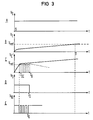
- the control unit supplies on its output pin S a signal commanding the switching on the load 2, this unit simultaneously sends to the input pin 9 of the pre-charge sub-circuit 8 a validation signal of predetermined duration To (see Figure 3 Graph D).
- This signal is received by a logic AND gate 12 which has a second input connected at 10 to the output of the comparator 6.
- the comparator 6 supplies a "high" level logic signal indicating that the voltage at the terminals of the load 2 is then less than Vref because of the starting of the charging of the capacitor C of the filter 3.
- the AND gate then immediately triggers the conduction of the transistor 7 which then causes the voltage V DD to be applied to the capacitor C which then charges very rapidly.
- the output of the comparator 6 is connected to an input pin 13 of the control unit.
- the control unit receives a "low" signal from the comparator representative of the absence of a short-circuit of the load 2.
- Graph E shows the switchovers of the comparator between the instants Toc and To, these switchovers producing a regulation of the voltage V E about the value Vref between these two instants, because of the loopback of the circuit of the gate 12 and the transistor 7 by the comparator 6.
- this gate cuts off the transistor 7.
- the voltage V E then decreases because of the discharging of the capacitor C which is no longer charged neither by the source V DD nor by the source +Vbat because of the short-circuiting of the load 2.
- the output of the comparator then returns in a stable way to the high state to indicate the short-circuit of the load to the control unit 4.
- the value of the duration To of the validation pulse is set at 2 ⁇ s.
- the control unit is informed of the short-circuit of the load at the end of 2 ⁇ s, compared with a duration of T in the order of 200 ⁇ s of the corresponding delay for the circuit of the prior art shown in Figure 1.
- An important advantageous characteristic of the circuit according to the invention depends on the production by the control unit of the validation pulse of duration To ( Figure 3,D).
- the latter delays the production by the comparator of a signal representative of a state of short-circuit of the load by To.
- the value of To is chosen such that it is longer than Toc ( Figure 3, C), the time required for the charging of the capacitor C by the source V DD to reach the value Vref.
- Toc is a function of the capacitor C of the filter 3 external to the circuit 11. This filter 3 must be able to be adapted to modifications of the load of the actuator to be monitored, without this resulting in a modification of the circuit 11.
- the means of pre-charging the capacitor C built into the circuit can easily be integrated at low cost because they require the integration of only one logic gate and one MOS transistor.
Landscapes
- Engineering & Computer Science (AREA)
- Power Engineering (AREA)
- Testing Of Short-Circuits, Discontinuities, Leakage, Or Incorrect Line Connections (AREA)
- Emergency Protection Circuit Devices (AREA)
- Electronic Switches (AREA)
- Electrical Control Of Air Or Fuel Supplied To Internal-Combustion Engine (AREA)
- Combined Controls Of Internal Combustion Engines (AREA)
- Control Of Voltage And Current In General (AREA)
- Dc-Dc Converters (AREA)
- Testing Electric Properties And Detecting Electric Faults (AREA)
Description
- The present invention relates to a circuit for controlling the power supply of an electrical load provided with a device for detecting a short-circuit of the load. More particularly, the invention relates to such a circuit designed for controlling the power supply of an inductive load whose detecting device monitors the possible short-circuiting of the load in order that a corrective action may be triggered in response intended to prevent, for example, damage to the circuit by this short-circuit of the load or defective functioning of a unit fitted with this load.
- In motor vehicle electronics, numerous actuators comprise such inductive loads. There can be mentioned the winding of a fuel injector or that of an electrovalve varying the pressure of a braking fluid in an anti-locking device for the wheels of a vehicle. It is furthermore possible to mention the coil of an inductive primary ignition circuit.
- The circuits controlling such inductive loads in a motor vehicle environment are often fitted with diagnostic means enabling the detection, for example, of a disconnection or an accidental short-circuit of the inductive load rendering the latter inoperative, this detection being made for reasons of safety for example. These means comprise electronic circuits which monitor the voltage existing at the terminals of the load in order to detect, for example, the possible appearance of a short-circuit and to trigger alarm actions or appropriate corrective actions.
- Considering the high interference environment of a motor vehicle, the voltage sampled at the terminals of the load must be filtered in order that it may be used, the filtered signal being compared with a reference voltage. When the filtered signal is below this reference voltage, the means of comparison used trigger the supply of a signal representative of a short-circuited state of the load.
- Figure 1 of the accompanying drawing shows a circuit for controlling the power supply of an actuator having an inductive load, of the prior art. The circuit comprises a
power transistor 1 controlled by itsbase 5 in order to initiate the power supply of an inductive load 2 connected in series with the emitter-collector circuit of the power transistor, between the collector of the latter and ground. In the circuit shown, the power supply voltage +Vbat is supplied by the battery of a motor vehicle. As has been seen above, a filter 3, for example a low pass capacitive filter, takes the voltage from the terminal which is common to the inductive load 2 and the collector of thetransistor 1 in order to filter out the interference from this signal before applying it to an input E of thecontrol unit 4 which is designed to use the signal received from the filter 3. Theunit 4 also controls the conduction of the power transistor via a terminal S connected to the base of this transistor, through anactuator control sub-circuit 5. - When the control unit triggers this conduction, it is clear that the capacitor C of the low pass filter 3 begins to charge with a certain time constant. In Figure 3 of the accompanying drawing, there is shown at A the control signal Vs of the
transistor 1 output at S by the control unit, and at B, the voltage VE at the terminals of the capacitor. Up to the instant T where VE reaches a value Vref of a reference voltage generated by thecontrol unit 4 in order to derive, from a comparison of the voltage at the terminals of the load 2 after filtering with this voltage Vref, the presence or absence of a short-circuit of this load, it is clear that this comparison is not significant since the voltage at the terminals of the load is constantly lower than Vref, even in the absence of a short-circuit. - It is therefore necessary to provide means for preventing the control unit from taking account of any short-circuit information up to the instant T.
- In order to do this it is possible to consider generating a delay of the output signal of the filter by analog or digital means. When the control unit conventionally comprises a microprocessor, the delay is obtained by means of a parallel loaded counter initialized by the microprocessor. Incidentally, using this assumption, the voltage signal at the terminals of the load could also be filtered by digital means.
- The masking logic necessary for obtaining a digital delay has the disadvantage of being expensive. In fact, the delay to be generated must in practice be able to reach values in the order of 200 µs which, for a resolution of 2 µs, involves the use of a parallel loaded 7-bit counter in order to be programmable, a requirement which additionally demands the presence of a 7-bit register and the associated logic. The assembly requires the integration of about 200 MOS transistors per counter resulting in an expensive production.
- Such a solution does not however enable a reduction in the length of the time interval during which a short-circuit of the load cannot be detected. As seen above, the generated delay must in practice be in the order of 200 µs, whereas experience shows that a short-circuit of the load for more than 100 µs not taken into account can affect the safety of the control circuit of the power supply of this load.
- It is therefore an object of the present invention to provide a circuit for controlling the power supply of an electrical load, comprising a device for detecting a short-circuit of the load, this circuit being provided with means enabling the duration during which a possible short-circuit of the load cannot be observed by the device to be reduced to the minimum.
- Another object of the present invention is to provide such an integrated circuit which is less expensive than that of the digital masking means mentioned above.
- Another object of the present invention is to provide such a device in which the characteristics of the device for detecting a short-circuit of the load are independent of those of the filter used for removing interference from the voltage sampled at the terminals of the load. Such a circuit is thus easily adapted to a modification of this filter.
- These objects of the invention, as well as others which will appear below, are achieved with a circuit for controlling the power supply of an electrical load, having a device for detecting a short-circuit of the load by comparison of a reference voltage with a voltage sampled at the terminals of the load and filtered in a capacitive filter, this circuit being characterized in that it comprises means, actuated by the switching on of the electrical load, for pre-charging the capacitor of the filter in order to initially establish on the output of this capacitor a voltage substantially equal to the reference voltage, the time constant of the charging of the capacitor by these means being low with respect to that which corresponds to the charging of this capacitor by the supply voltage of the load alone.
- These pre-charging means comprise a connecting transistor for connecting the capacitor of the filter to a pre-charging voltage source and a logic sub-circuit for triggering the conduction of the transistor when the load is switched on.
- In one embodiment of the circuit according to the invention, the comparison of the reference voltage with the voltage sampled at the terminals of the load is performed by a comparator whose inputs are respectively supplied by these voltages. The logic sub-circuit then comprises a logic AND gate having two inputs respectively connected to the output of the comparator and to a source of a validation signal of predetermined duration, the output of the AND gate supplying a control pin of the connecting transistor.
- The invention will now be described by way of example with reference to the accompanying drawing in which:
- Figure 1 is a diagrammatic representation of a circuit for controlling the power supply of an electrical load, provided with a device for detecting a short-circuit of the load, of the prior art,
- Figure 2 is a diagrammatic representation of a circuit for controlling the power supply of an electrical load, provided with a device for detecting a short-circuit of the load according to the present invention , and,
- Figure 3 shows graphs of the variations in time of voltages sampled in the circuits of Figures 1 and 2, these graphs being used for understanding the operation of the circuit according to the present invention.
- Reference is made to Figure 2 of the drawing in which the circuit shown again uses various elements of the circuit in Figure 1 which is part of the prior art, as explained in the preamble of the present description. In Figures 1 and 2 identical numbers denote identical or similar devices.
- In Figure 2, a
power transistor 1 controls the electrical power supply of a load 2. Thetransistor 1 can be a transistor of the MOS technology type, or of the bipolar technology type as shown in the drawing in which it takes the form of a PNP type transistor connected by its emitter to the + pole of an electrical power supply source. In motor vehicle electronics, this power supply source is the battery of the vehicle which therefore supplies a voltage + Vbat. The load 2, typically an inductive winding in motor vehicle electronics, is then in this case part of an actuator, for example, an electrovalve which varies the pressure or the flow rate of a fluid. Such an electrovalve can thus initiate a supply of liquid fuel at a given time, or cut off this supply at a given time. - Safety reasons lead to the monitoring of the correct operation of such an actuator and, for this purpose, the detecting of a possible disconnection or short-circuiting of its winding.
- For short-circuit detection, there is conventionally provided, as seen above, a device which samples the voltage at the terminals of the load 2 and which compares this voltage with a reference voltage Vref. When the sampled voltage is less than Vref it is derived from this that the load is short-circuited. The device then generates a signal processed by a
control unit 4 for triggering corrective actions. - The control unit typically comprises one or more microprocessors, memories and interfaces by which are received signals from sensors monitoring values associated with the functioning of the vehicle: engine intake pressure, speed of rotation of the engine, temperature of the air or of a cooling liquid etc... These signals are processed by the
unit 4 which generates control signals for actuators which enable the adjustment of certain operating parameters for example. Thus thecontrol unit 4 generates at its output S a signal for triggering the conduction or non-conduction of thetransistor 1 via acontrol sub-circuit 5 of the actuator of which the inductive load 2 is a part. - In motor vehicle electronics, in particular, the environment is highly disturbed. The short-circuit device detection must therefore be supplied by a signal from which the interference has been filtered out and which represents the voltage at the terminals of the load. For this purpose there is conventionally used a low pass capacitive filter 3 which comprises, for example, a capacitor C and a resistor R2 connected in parallel between the ground and one terminal of a resistor R1 whose other terminal is connected to the point common to the load 2 and the collector of the
power transistor 1. At the point E′, which is the point common to the capacitor C and to the resistor R1, there is therefore available a voltage signal which is free of interference and which is compared with the voltage Vref in acomparator 6 in order to detect the presence of the possible short-circuit of the load. - When the control unit triggers, by means of the
actuator control 5 and thetransistor 1, the power supply of the load, this power supply will also cause the charging of the capacitor C, through the resistor R1, with a time constant determined by the values of the resistors R1 and R2 and of the capacitor C. - If what then occurs in the circuit of the prior art shown in Figure 1 is examined in conjunction with graph B in Figure 3 which shows the variation of the voltage at the output E of the filter of this circuit starting from the switching on at t = 0 of the load 2, triggered by the signal Vs applied by the
control unit 4 at its output S, it can be seen that the voltage at E increases until it reaches, at the instant T, the value Vref at which thecontrol unit 4 of the circuit in Figure 1 compares the filtered voltage in order to derive, in the case of the filtered voltage exceeding this value, the absence of any short-circuit of the load 2. - Up to the instant T, with the filtered voltage remaining below Vref, the detection device could confuse this situation with that resulting from a genuine short-circuit, even in the absence of such a short-circuit of the load.
- In order to avoid such an erroneous detection, a masking of the information provided by the detection device is provided up to the instant T. In order to do this, it is possible to use an analog delay or digital masking means such as described in the preamble of the present description. The latter are expensive and do not solve the problem of the detection device not supplying significant information up to the instant T.
- Now if the load is already short-circuited at the instant t = 0, or if a short-circuit occurs between t = 0 and t = T, it is clear that the detection device of the circuit in Figure 1 is not capable of indicating this short-circuit before the instant T because of the masking.
- In motor vehicle electronics a value in the order of 200 µs is usually observed for the duration of the interval [0, T], taking into account the time constant of the filter necessary for a good removal of interference from the voltage signal sampled at the load.
- Now it has been observed that a short-circuit which remains uncorrected for more than about 100 µs could inflict damage on the circuit.
- According to the present invention such a situation is prevented by providing the detection device of the circuit with means, shown in Figure 2, which enable the time interval during which a short-circuit of the load cannot be indicated by the detection device to be reduced to a few microseconds only.
- These means comprise a voltage source VDD connected by means of a connection transistor 7 to the output terminal of the filter 3. The transistor 7 can, for example, be of the N channel MOS type, the source of the transistor being connected to the capacitor C, at the output of the filter, while the drain is connected to the voltage source VDD. The gate of the transistor is controlled by the output of a pre-charged
control logic sub-circuit 8, this sub-circuit comprising twoinputs control unit 4 and to the output of thecomparator 6. - The transistor 7, the
sub-circuit 8 and thecomparator 6 can be integrated with the control unit in order to form a single integrated circuit 11 controlling via its output pin S the switching on of the load 2, and receiving at its input pin E′ the filtered voltage signal sampled at the terminals of this load. This integrated circuit can of course comprise other input and/or output terminals in order to receive or to supply signals processed in the control unit for monitoring purposes or for the control of other functions. - The circuit according to the invention therefore operates as follows. When the control unit supplies on its output pin S a signal commanding the switching on the load 2, this unit simultaneously sends to the
input pin 9 of the pre-charge sub-circuit 8 a validation signal of predetermined duration To (see Figure 3 Graph D). This signal is received by a logic ANDgate 12 which has a second input connected at 10 to the output of thecomparator 6. As soon as the load 2 is switched on, thecomparator 6 supplies a "high" level logic signal indicating that the voltage at the terminals of the load 2 is then less than Vref because of the starting of the charging of the capacitor C of the filter 3. The AND gate then immediately triggers the conduction of the transistor 7 which then causes the voltage VDD to be applied to the capacitor C which then charges very rapidly. In fact, the resistance RDSON of the transistor 7 when it is conducting is very low with respect to Rl and R2 and the time constant RDSON x C of the charging of the capacitor by the voltage source VDD is also low. Because of this low time constant, the capacitor C charges very rapidly as shown in full line in Figure 3, Graph C, which shows the variation of the voltage VE on the input pin E′ of the circuit 11. The voltage Vref is reached at the instant Toc. - If the charge 2 is not then short-circuited, the voltage VE will continue to increase, which causes the output of the
comparator 6 to switch over to the low state. The ANDgate 12 cuts off and the transistor 7 stops conducting. The charging of the capacitor C of the filter 3 continues under the effect of the voltage +Vbat alone with the time constant of the filter 3 as shown in full line in graph C. - The output of the
comparator 6 is connected to aninput pin 13 of the control unit. Thus from the instant Toc the control unit receives a "low" signal from the comparator representative of the absence of a short-circuit of the load 2. - If the case of a load in a short-circuited state when this load is switched on is now considered, the voltage at E′ at the instant Toc will not continue to increase as shown in full line in the graph C but will decrease until it drops below the value Vref again, because the voltage +Vbat is then short-circuited at the input of the filter 3. This decrease causes the output of the comparator to switch over to the high state and therefore puts the transistor 7 back into conduction which recharges the capacitor C to the voltage Vref, causing another switchover of the comparator etc... In Figure 3, Graph E shows the switchovers of the comparator between the instants Toc and To, these switchovers producing a regulation of the voltage VE about the value Vref between these two instants, because of the loopback of the circuit of the
gate 12 and the transistor 7 by thecomparator 6. However, at the end of the validation pulse of duration To applied to theinput 9 of thegate 12, this gate cuts off the transistor 7. The voltage VE then decreases because of the discharging of the capacitor C which is no longer charged neither by the source VDD nor by the source +Vbat because of the short-circuiting of the load 2. The output of the comparator then returns in a stable way to the high state to indicate the short-circuit of the load to thecontrol unit 4. - According to one embodiment of the invention given by way of example, the value of the duration To of the validation pulse is set at 2 µs. Thus by means of the invention, the control unit is informed of the short-circuit of the load at the end of 2 µs, compared with a duration of T in the order of 200 µs of the corresponding delay for the circuit of the prior art shown in Figure 1.
- An important advantageous characteristic of the circuit according to the invention depends on the production by the control unit of the validation pulse of duration To (Figure 3,D). The latter delays the production by the comparator of a signal representative of a state of short-circuit of the load by To. The value of To is chosen such that it is longer than Toc (Figure 3, C), the time required for the charging of the capacitor C by the source VDD to reach the value Vref. Now Toc is a function of the capacitor C of the filter 3 external to the circuit 11. This filter 3 must be able to be adapted to modifications of the load of the actuator to be monitored, without this resulting in a modification of the circuit 11. Such modifications can result, for example, from a technological development of the actuator incorporating this load or from a reduction in the sensitivity of the short-circuit detection device to induced interference, such modifications normally resulting from the development of products in time through the efforts of their designers. By suitably choosing To in such a way that To remains longer than Toc, whatever the foreseeable development of the actuator and of the associated filter may be, the characteristics of this circuit 11 are fixed and this circuit can subsequently be adapted to the foreseeable modifications of the filter. The characteristics of the short-circuit detection device of the control circuit according to the invention are thus rendered independent of subsequent developments of the filter.
- The means of pre-charging the capacitor C built into the circuit can easily be integrated at low cost because they require the integration of only one logic gate and one MOS transistor.
- Because the time period To to be masked is extremely short with the circuit according to the invention, it is possible to almost completely dispense with the masking logic described in the preamble to the present invention, which logic can contain several hundred MOS transistors. The saving in area for the integrated circuit is therefore considerable.
- The safety and reliability of the control circuit according to the invention are greatly improved with respect to those of the circuit in Figure 1 (of the prior art), because the response time of the short-circuit detection device is reduced to very small values, much less than the critical value of 100 µs mentioned above.
- By way of example, for an implementation of the invention in a control circuit for an electrovalve to cut off the supply of the fuel, the following values have been selected for certain parameters of the circuit:

Claims (8)
- Circuit for controlling the power supply of an electrical load (2), having a device for detecting a short-circuit of the load by comparison of a reference voltage with a voltage sampled at the terminals of the load (2) and filtered in a capacitive filter (3), this circuit being characterized in that it comprises means (7, 8), actuated by the switching on of the electrical load, for pre-charging the capacitor (C) of the filter (3) in order to initially establish on the output of this capacitor a voltage substantially equal to the reference voltage, the time constant of the charging of the capacitor by these means being low with respect to that which corresponds to the charging of this capacitor by the supply voltage of the load (2) alone.
- Circuit according to Claim 1, characterized in that the said means comprise a connecting transistor (7) for connecting the capacitor (C) of the filter (3) to a pre-charging voltage source (VDD) and a logic sub-circuit (8) for triggering the conduction of the transistor (7) when the load is switched on.
- Circuit according to Claim 2, in which the inputs of a comparator (6) are respectively supplied by a source of reference voltage Vref and by the output voltage (VE) of the filter, characterized in that the logic sub-circuit (8) comprises a logic AND gate (12) having two inputs (10, 9) respectively connected to the output of the comparator (6) and to a source (4) of a validation signal of predetermined duration (To), the output of the AND gate being connected to a pin controlling the conduction of the connection transistor (7), the output of the comparator supplying a signal representative of a state of short-circuit of the load (2) when the output voltage of the filter remains below Vref at the end of the validation signal (To).
- Circuit according to Claim 3, characterized in that it comprises a control unit (4) connected to a control pin of a transistor (1) controlling the flow of a current between the positive terminal of a power supply source (+Vbat) of the load (2) and that load, this control unit (4) also being connected to the AND gate (12) of the logic sub-circuit, in order to supply to the control pin of the control transistor (1) a signal for putting that transistor into conduction and, simultaneously, a validation signal to the AND gate (12) of the logic sub-circuit (8).
- Circuit according to Claim 4, characterized in that the control unit (4), the comparator (6), the connection transistor (7) and the logic sub-circuit (8) controlling this transistor constitute a single integrated circuit (11), the capacitive filter (3) being external to this integrated circuit.
- Circuit according to any of Claims 3 to 5, characterized in that the duration To of the validation signal, starting from the switching on of the load (2) is longer than the duration Toc of the charging of the capacitor (C) to the reference voltage Vref, when this capacitor is connected by the connection transistor (7) to the pre-charging voltage source (VDD)
- Circuit according to any of the preceding Claims, characterized in that the capacitive filter is a low pass RC filter comprising a capacitor (C) and a resistor (R2) in parallel between the ground of the circuit and a terminal of a second resistor (R1) whose other terminal is connected to the load (2), at the end at which it is supplied, the other terminal of the load (2) being connected to ground.
- Circuit according to any of the preceding Claims, characterized in that the load is an inductive load forming part of an actuator.
Applications Claiming Priority (2)
| Application Number | Priority Date | Filing Date | Title |
|---|---|---|---|
| FR8807005 | 1988-05-26 | ||
| FR8807005A FR2632070B1 (en) | 1988-05-26 | 1988-05-26 | CIRCUIT FOR CONTROLLING THE POWER SUPPLY OF AN ELECTRIC CHARGE, WITH DEVICE FOR DETECTING A SHORT-CIRCUIT OF THE CHARGE |
Publications (2)
| Publication Number | Publication Date |
|---|---|
| EP0343536A1 EP0343536A1 (en) | 1989-11-29 |
| EP0343536B1 true EP0343536B1 (en) | 1993-03-17 |
Family
ID=9366639
Family Applications (1)
| Application Number | Title | Priority Date | Filing Date |
|---|---|---|---|
| EP89109088A Expired - Lifetime EP0343536B1 (en) | 1988-05-26 | 1989-05-19 | Circuit for controlling the power supply of an electrical load, having a device for detecting a short-circuit of the load |
Country Status (6)
| Country | Link |
|---|---|
| US (1) | US5187631A (en) |
| EP (1) | EP0343536B1 (en) |
| JP (1) | JPH0284813A (en) |
| DE (1) | DE68905378T2 (en) |
| ES (1) | ES2042874T3 (en) |
| FR (1) | FR2632070B1 (en) |
Families Citing this family (24)
| Publication number | Priority date | Publication date | Assignee | Title |
|---|---|---|---|---|
| JPH0812890B2 (en) * | 1988-05-24 | 1996-02-07 | 富士通株式会社 | Module sealing method |
| US5636097A (en) * | 1991-05-09 | 1997-06-03 | Consorzio Per La Ricerca Sulla Microelettronica | Protective circuit for semiconductor power device |
| IT1248382B (en) * | 1991-05-09 | 1995-01-11 | Cons Ric Microelettronica | PROTECTION CIRCUIT AGAINST INCREASED OUTPUT CURRENT FOR AN INTEGRATED CIRCUIT INCLUDING A POWER DEVICE THAT DRIVES A RESONANT LOAD CONNECTED TO A POWER SUPPLY |
| JPH06203189A (en) * | 1992-12-28 | 1994-07-22 | Takayama:Kk | Divider circuit |
| ES2107337B1 (en) * | 1994-07-05 | 1998-07-01 | Univ Catalunya Politecnica | AUTOMATIC ELECTRIC LINE DISCONNECTION DEVICE BELOW A MINIMUM AND CONNECTION WITH PRE-CHECKING OF SHORT CIRCUIT AND OVERLOAD. |
| US5754569A (en) * | 1996-05-29 | 1998-05-19 | Sun Microsystems, Inc. | Apparatus and method for comparing and validating digital words |
| US5828261A (en) * | 1996-11-13 | 1998-10-27 | Caterpillar Inc. | Gate drive circuit that controls a power transistor in three states |
| DE69737102T2 (en) * | 1997-10-08 | 2007-07-05 | Mitsubishi Denki K.K. | CONTROL FOR A VEHICLE |
| DE19754126A1 (en) * | 1997-12-05 | 1999-06-17 | Siemens Ag | Circuit arrangement for controlling an electrical drive unit |
| DE19813103A1 (en) * | 1998-03-25 | 1999-09-30 | Bosch Gmbh Robert | Method and device for controlling a consumer |
| DE19911863A1 (en) * | 1999-03-17 | 2000-09-21 | Philips Corp Intellectual Pty | Circuit arrangement for controlling actuator for supplying electrical energy to it used in IC engine has actuator which in its first connection is connected between first current control element and first bypass element |
| AU7119600A (en) * | 1999-09-10 | 2001-04-10 | Intra International Ab | System and method for providing surge, short and reverse polarity connection protection |
| IES20020511A2 (en) * | 2002-06-24 | 2003-05-14 | Hi Key Ltd | A monitoring circuit for determining the state of a device, and a current emulating circuit for emulating current drawn by the device |
| FR2853475B1 (en) * | 2003-04-01 | 2005-07-08 | Atmel Nantes Sa | INTEGRATED CIRCUIT DELIVERING LOGIC LEVELS AT AN INDEPENDENT VOLTAGE OF THE POWER SUPPLY VOLTAGE, WITHOUT AN ASSOCIATED REGULATOR FOR THE POWER SECTION, AND CORRESPONDING COMMUNICATION MODULE |
| US20050088239A1 (en) * | 2003-10-23 | 2005-04-28 | Tai Jy-Der D. | Short-circuit detecting and protecting circuit for integrated circuit |
| CN100339630C (en) * | 2004-03-12 | 2007-09-26 | 华硕电脑股份有限公司 | Solenoid valve protection circuit |
| DE102005055832A1 (en) * | 2005-11-23 | 2007-05-24 | Patent-Treuhand-Gesellschaft für elektrische Glühlampen mbH | Circuit arrangement for controlling electronic component, has bipolar transistor provided in grounded-base circuit and having emitter coupled with output of microprocessor, and another bipolar transistor provided in grounded-emitter circuit |
| GB2453447A (en) * | 2007-04-27 | 2009-04-08 | Cambridge Semiconductor Ltd | A protection scheme for a switched-mode power converter |
| CN105207461B (en) * | 2015-09-16 | 2018-12-25 | 杭州华为数字技术有限公司 | A kind of control system that having delayed circuit, control method and control device |
| US12474415B2 (en) | 2020-10-28 | 2025-11-18 | Halo Microelectronics International | Short circuit detection apparatus and control method for switched capacitor converter |
| US11740300B2 (en) * | 2020-10-28 | 2023-08-29 | Halo Microelectronics International | Short circuit detection apparatus and control method for switched capacitor converter |
| CN113937725B (en) * | 2021-09-07 | 2025-02-07 | 华为数字能源技术有限公司 | Short-circuit protection device, short-circuit protection method for target circuit, and power conversion equipment |
| CN113497551B (en) * | 2021-09-07 | 2022-01-14 | 天津海翼科技有限公司 | Direct-current power supply multi-path output protection circuit unit, protection circuit and underwater robot |
| CN118348374B (en) * | 2024-03-28 | 2024-10-01 | 海信家电集团股份有限公司 | Test circuit and test device thereof |
Family Cites Families (9)
| Publication number | Priority date | Publication date | Assignee | Title |
|---|---|---|---|---|
| US3733540A (en) * | 1972-02-03 | 1973-05-15 | Motorola Inc | Switching regulator sweep starting protection circuit |
| US4016461A (en) * | 1976-05-06 | 1977-04-05 | Amp Incorporated | Starting circuit for switching regulator |
| US4106498A (en) * | 1976-12-27 | 1978-08-15 | American Optical Corporation | Initialization circuit |
| DE3042138A1 (en) * | 1980-11-03 | 1982-05-27 | Mannesmann AG, 4000 Düsseldorf | PROTECTIVE CIRCUIT DEVICE FOR A DC MOTOR, ESPECIALLY FOR A PRINTER REWINDING DC MOTOR |
| DE3104015C2 (en) * | 1981-02-05 | 1984-10-11 | Siemens AG, 1000 Berlin und 8000 München | Overcurrent protection arrangement for a semiconductor switch |
| US4574232A (en) * | 1983-10-21 | 1986-03-04 | Motorola, Inc. | Rapid turn-on voltage regulator |
| DE3346435A1 (en) * | 1983-12-22 | 1985-08-14 | Robert Bosch Gmbh, 7000 Stuttgart | CIRCUIT ARRANGEMENT FOR SWITCHING ON AND OFF AND FOR MONITORING ELECTRICAL CONSUMERS |
| DE3702517A1 (en) * | 1987-01-28 | 1988-08-11 | Mitec Moderne Ind Gmbh | CIRCUIT ARRANGEMENT FOR POWERING A VARIETY OF CONSUMERS |
| US4816963A (en) * | 1987-12-21 | 1989-03-28 | General Motors Corporation | Apparatus for protecting a transistor in the event of a shorted load condition |
-
1988
- 1988-05-26 FR FR8807005A patent/FR2632070B1/en not_active Expired - Lifetime
-
1989
- 1989-05-19 DE DE8989109088T patent/DE68905378T2/en not_active Expired - Lifetime
- 1989-05-19 ES ES89109088T patent/ES2042874T3/en not_active Expired - Lifetime
- 1989-05-19 EP EP89109088A patent/EP0343536B1/en not_active Expired - Lifetime
- 1989-05-26 JP JP1131666A patent/JPH0284813A/en active Pending
- 1989-05-26 US US07/357,261 patent/US5187631A/en not_active Expired - Lifetime
Also Published As
| Publication number | Publication date |
|---|---|
| DE68905378D1 (en) | 1993-04-22 |
| DE68905378T2 (en) | 1993-08-26 |
| FR2632070B1 (en) | 1990-11-23 |
| EP0343536A1 (en) | 1989-11-29 |
| FR2632070A1 (en) | 1989-12-01 |
| ES2042874T3 (en) | 1993-12-16 |
| US5187631A (en) | 1993-02-16 |
| JPH0284813A (en) | 1990-03-26 |
Similar Documents
| Publication | Publication Date | Title |
|---|---|---|
| EP0343536B1 (en) | Circuit for controlling the power supply of an electrical load, having a device for detecting a short-circuit of the load | |
| US5430438A (en) | Method and device for functional monitoring of an electrical load | |
| US4433390A (en) | Power processing reset system for a microprocessor responding to sudden deregulation of a voltage | |
| US4630840A (en) | Vehicle height adjusting device | |
| US4737761A (en) | Feeding of electrical energy to circuits on a wheel for a tire-monitoring device | |
| US6411481B1 (en) | Method and device for suppressing over-voltages | |
| US5376854A (en) | Device for detecting failure in piezoelectric apparatus | |
| CA2061762A1 (en) | Airbag triggering system | |
| US5587865A (en) | Electronic control equipment for motor vehicles, particularly, electronic brake control equipment | |
| US5075627A (en) | Circuit apparatus for measuring the primary voltage of an ignition coil | |
| US5936361A (en) | Discharge lamp lighting circuit with lighting condition detector | |
| US5218339A (en) | Arrangement for monitoring a consumer in combination with an internal combustion engine and/or a motor vehicle | |
| US4017765A (en) | Short circuit protected electronic control system | |
| US5519643A (en) | Method of operating a microprocessor | |
| US4467762A (en) | Control apparatus for a fuel metering system | |
| KR900009784Y1 (en) | Starter motor control device for engine | |
| US5973416A (en) | Method for controlling a power supply switch and circuit arrangement for performing the control | |
| EP0485119A2 (en) | Circuit for driving a load and for producing a signal indicative of the condition of the load | |
| US4147145A (en) | Ignition coil current control circuit | |
| EP0954079B1 (en) | Bidirectional electronic switch | |
| JP2004312996A (en) | Protective device to polarity reversal | |
| US9783139B2 (en) | Switch monitoring circuit | |
| US5479314A (en) | Circuit arrangement having a semiconductor switch for the switching of a load | |
| JPH06232712A (en) | Protection device for load controller | |
| US4280166A (en) | Over-voltage protected solid-state ignition system |
Legal Events
| Date | Code | Title | Description |
|---|---|---|---|
| PUAI | Public reference made under article 153(3) epc to a published international application that has entered the european phase |
Free format text: ORIGINAL CODE: 0009012 |
|
| AK | Designated contracting states |
Kind code of ref document: A1 Designated state(s): DE ES GB IT NL SE |
|
| 17P | Request for examination filed |
Effective date: 19900226 |
|
| 17Q | First examination report despatched |
Effective date: 19920427 |
|
| GRAA | (expected) grant |
Free format text: ORIGINAL CODE: 0009210 |
|
| AK | Designated contracting states |
Kind code of ref document: B1 Designated state(s): DE ES GB IT NL SE |
|
| REF | Corresponds to: |
Ref document number: 68905378 Country of ref document: DE Date of ref document: 19930422 |
|
| PGFP | Annual fee paid to national office [announced via postgrant information from national office to epo] |
Ref country code: SE Payment date: 19930512 Year of fee payment: 5 |
|
| PGFP | Annual fee paid to national office [announced via postgrant information from national office to epo] |
Ref country code: NL Payment date: 19930531 Year of fee payment: 5 |
|
| ITF | It: translation for a ep patent filed | ||
| REG | Reference to a national code |
Ref country code: ES Ref legal event code: FG2A Ref document number: 2042874 Country of ref document: ES Kind code of ref document: T3 |
|
| PLBE | No opposition filed within time limit |
Free format text: ORIGINAL CODE: 0009261 |
|
| STAA | Information on the status of an ep patent application or granted ep patent |
Free format text: STATUS: NO OPPOSITION FILED WITHIN TIME LIMIT |
|
| 26N | No opposition filed | ||
| PG25 | Lapsed in a contracting state [announced via postgrant information from national office to epo] |
Ref country code: SE Effective date: 19940520 |
|
| PG25 | Lapsed in a contracting state [announced via postgrant information from national office to epo] |
Ref country code: NL Effective date: 19941201 |
|
| NLV4 | Nl: lapsed or anulled due to non-payment of the annual fee | ||
| EUG | Se: european patent has lapsed |
Ref document number: 89109088.8 Effective date: 19941210 |
|
| EUG | Se: european patent has lapsed |
Ref document number: 89109088.8 |
|
| REG | Reference to a national code |
Ref country code: GB Ref legal event code: IF02 |
|
| PGFP | Annual fee paid to national office [announced via postgrant information from national office to epo] |
Ref country code: DE Payment date: 20080620 Year of fee payment: 20 Ref country code: ES Payment date: 20080529 Year of fee payment: 20 |
|
| PGFP | Annual fee paid to national office [announced via postgrant information from national office to epo] |
Ref country code: IT Payment date: 20080527 Year of fee payment: 20 |
|
| PGFP | Annual fee paid to national office [announced via postgrant information from national office to epo] |
Ref country code: GB Payment date: 20080512 Year of fee payment: 20 |
|
| REG | Reference to a national code |
Ref country code: GB Ref legal event code: PE20 Expiry date: 20090518 |
|
| REG | Reference to a national code |
Ref country code: ES Ref legal event code: FD2A Effective date: 20090520 |
|
| PG25 | Lapsed in a contracting state [announced via postgrant information from national office to epo] |
Ref country code: ES Free format text: LAPSE BECAUSE OF EXPIRATION OF PROTECTION Effective date: 20090520 |
|
| PG25 | Lapsed in a contracting state [announced via postgrant information from national office to epo] |
Ref country code: GB Free format text: LAPSE BECAUSE OF EXPIRATION OF PROTECTION Effective date: 20090518 |