EP0127187A2 - Power converter - Google Patents
Power converter Download PDFInfo
- Publication number
- EP0127187A2 EP0127187A2 EP84106203A EP84106203A EP0127187A2 EP 0127187 A2 EP0127187 A2 EP 0127187A2 EP 84106203 A EP84106203 A EP 84106203A EP 84106203 A EP84106203 A EP 84106203A EP 0127187 A2 EP0127187 A2 EP 0127187A2
- Authority
- EP
- European Patent Office
- Prior art keywords
- thyristors
- thyristor
- coupled
- power
- circuit
- Prior art date
- Legal status (The legal status is an assumption and is not a legal conclusion. Google has not performed a legal analysis and makes no representation as to the accuracy of the status listed.)
- Granted
Links
Images


Classifications
-
- H—ELECTRICITY
- H02—GENERATION; CONVERSION OR DISTRIBUTION OF ELECTRIC POWER
- H02M—APPARATUS FOR CONVERSION BETWEEN AC AND AC, BETWEEN AC AND DC, OR BETWEEN DC AND DC, AND FOR USE WITH MAINS OR SIMILAR POWER SUPPLY SYSTEMS; CONVERSION OF DC OR AC INPUT POWER INTO SURGE OUTPUT POWER; CONTROL OR REGULATION THEREOF
- H02M7/00—Conversion of ac power input into dc power output; Conversion of dc power input into ac power output
- H02M7/02—Conversion of ac power input into dc power output without possibility of reversal
- H02M7/04—Conversion of ac power input into dc power output without possibility of reversal by static converters
- H02M7/12—Conversion of ac power input into dc power output without possibility of reversal by static converters using discharge tubes with control electrode or semiconductor devices with control electrode
- H02M7/145—Conversion of ac power input into dc power output without possibility of reversal by static converters using discharge tubes with control electrode or semiconductor devices with control electrode using devices of a thyratron or thyristor type requiring extinguishing means
- H02M7/155—Conversion of ac power input into dc power output without possibility of reversal by static converters using discharge tubes with control electrode or semiconductor devices with control electrode using devices of a thyratron or thyristor type requiring extinguishing means using semiconductor devices only
- H02M7/162—Conversion of ac power input into dc power output without possibility of reversal by static converters using discharge tubes with control electrode or semiconductor devices with control electrode using devices of a thyratron or thyristor type requiring extinguishing means using semiconductor devices only in a bridge configuration
- H02M7/1623—Conversion of ac power input into dc power output without possibility of reversal by static converters using discharge tubes with control electrode or semiconductor devices with control electrode using devices of a thyratron or thyristor type requiring extinguishing means using semiconductor devices only in a bridge configuration with control circuit
Abstract
Description
- The present invention relates to a power converter for converting AC power to DC power or converting the frequency of AC power to a different frequency and, more particularly, relates to a power converter having a function to reduce reactive power of an AC power supply.
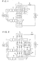
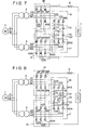
- Fig. 1 shows a circuit configuration of a power converter which involves a problem to be solved by the present invention. An
AC power supply 1 is connected to the primary of each of first andsecond power transformers transformer 2 is connected to a first thyristor bridge 4 being formed of GTO (gate turn-off) or self-extinction type thyristors. The secondary oftransformer 3 is connected to asecond thyristor bridge 5 being formed of general thyristors.Reference numeral 6 denotes a filtering power reactor, 7 denotes a load, and 8 denotes a surge absorbing circuit consisting of resistors and capacitors. In this circuit configuration, the triggering for first thyristor bridge 4 is controlled in a phase-advanced mode, while the triggering forsecond thyristor bridge 5 is controlled in a phase-delayed mode. Then, phase-advanced reactive power and phase-delayed reactive power generated by the respective thyristor bridges are cancelled, so that the reactive power ofAC power supply 1 is reduced. Thus, the power converter of Fig. 1 can operate with a unity power factor for the fundamental wave. - In the configuration of Fig. 1, when the thyristor bridge is controlled in a general phase-delayed mode, a commutation is performed, without requiring a self-extinction function to the thyristors, by simply triggering the thyristor to be supplied with a current of next triggering sequence. In this case, a current flow is shifted or commutated from the thyristor in a current feeding state to the thyristor to be triggered next, and the current feeding phase of the power supply is changed. Such a commutation is called a natural commutation. According to a natural commutation, a . current is sequentially switched in accordance with the difference in the phase voltages of
power sources - In contrast to the above, when the thyristor bridge is controlled in a phase-advanced mode, phase- advance/phase-delay relations of the phase voltages from
power sources - Fig. 2 shows a circuit configuration of another power converter whose power conversion efficiency is improved, but it still involves a problem to be solved. The circuit configuration of Fig. 2 is substantially identical to that disclosed in Fig. 4 of Japanese Patent Publication No. 51-22606. The surge absorbing circuit of Fig. 2 is formed of a rectifier 9, capacitor 10, filtering reactor 11, thyristor bridge 12, and
transformer 13. A surge voltage generated is rectified by rectifier 9 and the rectified voltage is temporarily stored in capacitor 10. The energy stored in capacitor 10 is regenerated topower supply 1 via filtering reactor 11, thyristor bridge 12 andtransformer 13 according to the inverting operation of thyristor bridge 12. In this circuit, although the power conversion efficiency is improved, a bulky device for surge absorption is required. The power converter thus becomes large in size and high in manufacturing cost. This is the problem of the configuration of Fig. 2. - It is accordingly the object of the present invention to provide a power converter which can reduce the reactive power of a power supply, avoid the generation of a surge voltage, improve the power conversion efficiency, and allow a simple circuit configuration.
- To achieve the above object, the power converter of the present invention utilizes first and second thyristor bridges energized by two AC power sources which are insulated from each other. The power converter is provided with a commutation circuit and first and second auxiliary thyristor circuits. Each of these auxiliary thyristor circuits includes plural thyristors. One terminal (e.g., cathode) of each thyristor of first auxiliary thyristor circuit is connected to one of the AC power sources, and the other terminals (e.g., anode) of respective thyristors are connected each other at a common node. One terminal (e.g., anode) of each thyristor of second auxiliary thyristor circuit is connected to the other of the AC power sources, and the other terminals (e.g., cathode) of respective thyristors are connected each other at another common node. The commutation circuit is connected between the common nodes of the first and second auxiliary thyristor circuits.
- This invention can be more fully understood from the following detailed description when taken in conjunction with the accompanying drawings, in which:
- Fig. 1 shows a circuit configuration of a power converter which involves a problem to be solved by the present invention;
- Fig. 2 shows a circuit configuration of another power converter whose power conversion efficiency is improved, but it still involves a problem to be solved;
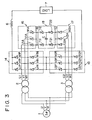
- Fig. 3 shows a circuit configuration of a first embodiment of the present invention, which is applied to a three-phase AC power supply;
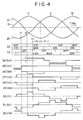
- Fig. 4 is a timing chart explaining the basic operation for reducing reactive power according to the configuration of Fig. 3;
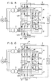
- Figs. 5 to 7 illustrate the current path for explaining the commutation operation of the configuration of Fig. 3, wherein Fig. 5 illustrates the current flow around time tl in Fig. 4, Fig. 6 shows the current path after inversion of the voltage polarity of capacitor C, and Fig. 7 shows the current path around time t2 in Fig. 4;
- Fig. 8 shows a circuit configuration of a second embodiment of the present invention;
- Fig. 9 shows a circuit configuration of a third embodiment of the present invention;
- Fig. 10 shows a circuit configuration of a fourth embodiment of the present invention;
- Fig. 11 shows a circuit configuration of a fifth embodiment of the present invention;
- Fig. 12 shows details of a trigger control circuit which may be adapted for controlling the operation of the embodiment;
- Fig. 13 shows a timing chart illustrating the operation of the circuit of Fig. 12;
- Fig. 14 shows a modification of the embodiment of Fig. 3, which is applied to a single-phase AC power supply; and
- Fig. 15 shows another modification of the embodiment of Fig. 3, which is applied to a polyphase (four-phase) AC power supply.
- The present invention will now be described with reference to the accompanying drawings. Fig. 3 shows a circuit configuration of a first embodiment of the present invention.
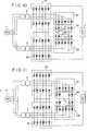
AC power supply 1,first transformer 2,second transformer 3,filtering reactor 6 andload 7 may be the same as those shown in Fig. 1 or 2. Afirst thyristor bridge 14 is energized by the secondary output voltages Ul, V1 and W1 fromfirst transformer 2.Thyristor bridge 14 is formed of general (conventional) thyristors U1P, V1P, W1P, U1N, V1N and WIN. Asecond thyristor bridge 15 is energized by the secondary output voltages U2, V2 and W2 fromsecond transformer 3.Thyristor bridge 15 is formed of general thyristors U2P, V2P, W2P, U2N, V2N and W2N. - A first
auxiliary thyristor circuit 16 is formed of general thyristors UlA, VIA and W1A. The cathodes of thyristors U1A, VIA and W1A respectively receives the secondary output voltages Ul, VI and Wl fromfirst transformer 2. The anode of each of thyristors U1A, VIA and W1A is connected to a common node N1. A secondauxiliary thyristor circuit 17 is formed of general thyristors U2A, V2A and W2A. The anodes of thyristors U2A, V2A and W2A respectively receives the secondary output voltages U2, V2 and W2 fromsecond transformer 3. The cathode of each of thyristors U2A, V2A and W2A is connected to a common node N2. Acommutation circuit 18 is inserted between the common nodes N1 and N2.Commutation circuit 18 is formed of a capacitor C and a thyristor bridge of general thyristors Tll, T12, T21 and T22. One end of capacitor C is connected to the junction between the anode of thyristor T11 and the cathode of thyristor T21. The other end of capacitor C is connected to the junction between the anode of thyristor T12 and the cathode of thyristor T22. The cathode of each of thyristors T11 and T12 is connected . to common node Nl. The anode of each of thyristors T21 and T22 is connected to common node N2. - The power converter of Fig. 3 will operate as follows. Fig. 4 is a timing chart explaining the basic operation for reducing reactive power. In Fig. 4, details of the waveform during commutation are omitted. (Details thereof will be described later with reference to Fig. 13.) For the sake of simplicity, each turns ratio between the primary and secondary windings of
transformers AC power supply 1,first transformer 2 andsecond transformer 3 may be represented by awaveform 19 as shown in Fig. 4. Similarly, voltage waveforms of other phases V (VI, V2) and W (Wl, W2) may be represented bywaveforms Numeral 22 indicates the conduction state offirst thyristor bridge 14, and numeral 23 indicates the conduction state ofsecond thyristor bridge 15. Symbols W1P, VIN, U2P, ect., indicate the conduction periods of corresponding thyristors in Fig. 3. - Positive side thyristors UlP, V1P and W1P of
first thyristor bridge 14 are controlled with a control angle a in a phase-delayed mode. Negative side thyristors U1N, VIN and W1N offirst thyristor bridge 14 are controlled with a control angle -a in a phase-advanced mode. Positive side thyristors U2P, V2P and W2P ofsecond thyristor bridge 15 are controlled with control angle -a in a phase-advanced mode. Negative side thyristors U2N, V2N and W2N ofsecond thyristor bridge 15 are controlled with control angle a in a phase-delayed mode. The conduction states 22 and 23 in Fig. 4 are illustrated for the control angle of a. In Fig. 3, it is assumed that the inductance of filteringreactor 6 is sufficiently large so that a constant load current I flows.Numerals first transformer 2.Numerals second transformer 3.Numerals AC power supply 1. - As may be seen from
current waveforms voltage waveforms - The commutation operation of Fig. 3 configuration will be as follows. A commutation from thyristor V1N to thyristor W1N of
first thyristor bridge 14, which is controlled in a phase-advanced mode at time tl in Fig. 4, will first be described. - Fig. 5 illustrates the current flow in the configuration of Fig. 3 around time tl in Fig. 4. Just before time tl, a first current path is formed through blacked-out thyristors V2N, U2P, V1N and W1P. This first current path is indicated by the solid line. Capacitor C of
commutation circuit 18 has been charged with the illustrated polarity. At time tl, thyristors T11 and T22 incommutation circuit 18 and auxiliary thyristors VIA and U2A are turned on. Then, a second current path including hatched thyristors U2A and T22, capacitor C and hatched thyristors T11 and VIA is established. This second current path is indicated by the broken line and is parallel to the first current path of thyristors U2P and V1N. The second current path is associated with a voltage being higher by the voltage stored in capacitor C than a voltage of the first current path. Due to this higher voltage, the current flow is instantaneously switched from the first current path (solid line) to the second current path (broken line). Then, the voltage of capacitor C is applied as a reverse bias voltage to thyristors U2P and VIN so that these thyristors are rendered nonconductive. Following to this, capacitor C is discharged by load current I and the polarity of capacitor C is inverted. In the above operation, although the current path is switched, the amount of the current flowing throughtransformers - Fig. 6 shows the current path after inversion of the voltage polarity of capacitor C. When thyristors U2P and WIN are triggered, a current path indicated by the broken line and including thyristors U2P and WIN is established. Then, the voltage of capacitor C is applied between the VI phase and the W1 phase of outputs from
first transformer 2, so that the voltage potential of W1 phase increases toward the positive side. The voltage differences between V and W phases ofAC power supply 1 and the voltage of capacitor C are applied to the leakage inductance offirst transformer 2. The current indicated by the solid line and flowing through auxiliary thyristors U2A and VIA is reduced at a rate which is determined by the above voltage differences, voltage of capacitor C and leakage inductance. At the same time, the current indicated by the broken line and flowing through thyristors U2P and W1N increases. When the current flowing through the thyristor bridges 14 and 15 becomes equal to the load current I, the current flowing through theauxiliary thyristors - Subsequently, at time t2 in Fig. 4, a commutation from thyristor W1P to thyristor UlP is performed. Fig. 7 shows the current path around time t2. Just before time t2 and after the commutation from thyristor V1N to thyristor WIN is completed as described above, a current path indicated by the solid line and including thyristors V2N, U2P, WIN and W1P is established. The subsequent commutation from thyristor W1P to thyristor U1P is performed in a general phase-delayed mode. A current path indicated by the broken line is then established at time t2, by merely triggering the thyristor U1P. The above commutation is performed in accordance with a current change rate which is determined by the voltage difference between the W and V phases of
AC power supply 1 and by the leakage inductance offirst transformer 2. When the commutation is completed, the current flowing through thyristor W1P becomes zero, and the current path is established to allow the load current to flow through thyristor U1P. - At time t3 in Fig. 4,
second thyristor bridge 15 is controlled in a phase-advanced mode and a commutation from thyristor U2P to thyristor V2P insecond thyristor bridge 15 is carried out. Then, auxiliary thyristors W1A and U2A and thyristors T12 and T21 ofcommutation circuit 18 are turned on. As in the case of commutation at time tl in a phase-advanced mode, a current path is shifted by means of the voltage of capacitor C to another current path including the auxiliary thyristors. The polarity of voltage of capacitor C is then inverted. When thyristors V2P and W1N are turned on under this voltage polarity inversion, the current path is shifted to the thyristor bridge side by the inverted voltage of capacitor C, thereby completing the commutation. - A commutation for thyristors which are controlled in a phase-delayed mode may be similarly performed by sequentially supplying triggering pulses to thyristors to be turned on. A commutation for thyristors which are controlled in a phase-advanced mode may be performed in the following manner. Two
auxiliary thyristors commutation circuit 18 are turned on in accordance with the charged voltage polarity of capacitor C. Then, the current path is temporarily shifted to the side of the auxiliary thyristors. After the inversion of the voltage polarity of capacitor C is completed, triggering pulses are supplied to two thyristors, which are to'be turned on next, of thyristor bridges 14 and 15. - As may be understood from the above description, a commutation for thyristors controlled in a phase-advanced mode is performed at a moderate current change rate as in the case of a commutation for thyristors controlled in a phase-delayed mode. Accordingly, a voltage in excess of the charged voltage of capacitor C is never applied to the power supply. Further, capacitor C is repeatedly charged/discharged at each commutation for thyristors in a phase-advanced mode. For this reason, capacitor C may only be charged initially, and the circuit of Fig. 3 does not require any resistors as used in surge absorbing circuit 8 of Fig. 1. Therefore, the power converter of Fig. 3 can minimize power loss. Further, as illustrated by the solid line in Fig. 7, a current path excluding one (2) of power transformers is formed within a certain control phase angle. This enables to reduce the power loss of the transformer.
- Fig. 8 shows a circuit configuration of a second embodiment of the present invention. The second embodiment of Fig. 8 is different from the first embodiment of Fig. 3 only in the configuration of the commutation circuit. Thus, a
commutation circuit 33 of the second embodiment is further provided with a reactor L and cross-coupled inversion thyristors X1 and X2. The mode of operation of the second embodiment is basically the same as that of the first embodiment. In the first embodiment, the inversion of the capacitor voltage incommutation circuit 18 is performed by a current having a magnitude being equal to the load current I. From this, when the amount of load current I is very small, a substantial time is required to complete the voltage inversion of capacitor C, thereby adversely affecting the commutation operation of next sequence. - To avoid unreliable commutation operation due to the above, the following-means is employed in the second embodiment. That is, after the current is shifted or commutated to the auxiliary thyristors and a certain period of time elapses, thyristor Xl or X2 is triggered in accordance with the voltage polarity of capacitor C. In other words, the polarity of the capacitor voltage is inverted by means of a resonance of reactor L and capacitor C. Simply stated, thyristor X1 or X2 is turned on when a given period of time (cf. T in Fig. 13N) has elapsed after the completion of triggering of the auxiliary thyristors (UlA, VIA, W1A, U2A, V2A, W2A) and the commutation thyristors (T11, T12, T21, T22).
- Fig. 9 shows a circuit configuration of a third embodiment of the present invention. The circuit of the third embodiment is different from that of the first and second embodiments in Figs. 3 and 8, only in the configuration of the commutation circuit. A
commutation circuit 34 of the third embodiment is formed of GTO thyristors GT1 and GT2, diodes Dl and D2, and capacitor C. In the second embodiment (Fig. 8), power loss due to the inversion of the capacitor voltage becomes prominent when the load current is small. In theory, no power loss appears with the inversion of the capacitor voltage. However, in practice, each of the reactor and capacitor includes resistive components, and voltage drops are inevitably involved with thyristors in turned-on state. Accordingly, a certain power loss cannot be avoided. The third embodiment is proposed to reduce such power loss and to remove the need for inverting the capacitor voltage. Capacitor C ofcommutation circuit 34 has a larger capacitance than those in the first and second embodiments and is initially charged in the polarity as indicated in Fig. 9. In order to perform a commutation for thyristors controlled in a phase-advanced mode, two auxiliary thyristors are turned on as in the former embodiments and, at the same time, GTO thyristors GT1 and GT2 ofcommutation circuit 34 are also turned on. Then, a current path is established to discharge the capacitor C. By the discharged capacitor voltage, the current path is temporarily shifted from the thyristor bridge side to the auxiliary thyristor side. - After elapsing a certain period of time corresponding to the turn-off time of a thyristor in turned-on state, extincting (OFF) pulses are supplied to GTO thyristors GT1 and GT2. At the same time, triggering (ON) pulses are supplied to two series thyristors, which are to be triggered next, in the thyristor bridge. When thyristors GT1 and GT2 are turned off, the current, which has been flowing through the auxiliary thyristors, now flows via diodes O1 and D2 in the direction to charge the capacitor C. Then, the relationship between the capacitor voltage and the current after the polarity inversion of the capacitor voltage is established as in the first and second embodiments. Thus, the current which has been flowing to the auxiliary thyristors is now commutated to the thyristor bridge. During this commutating time period, capacitor C is charged. If the ON period of GTO thyristors GTl and GT2 is suitably controlled in accordance with the charged voltage of capacitor C, the discharged voltage can be made equal to the charged voltage. In this case, the capacitor voltage can be kept substantially constant by mere initial charging of capacitor C. GTO thyristors GT1 and GT2 may be replaced with conventional bipolar transistors or with conventional thyristors being provided with a forced commutation circuit.
- Fig. 10 shows a circuit configuration of a fourth embodiment of the present invention. The fourth embodiment is used for converting AC power of a given frequency to AC power of another frequency. The fourth embodiment of Fig. 10 is constructed based on the second embodiment of Fig. 8, wherein a bidirectional current or AC current is supplied to an
AC load 7. The thyristors shown in Fig. 8 are replaced by two cross-coupled (inversely-parallel-connected) thyristors. (Each cross-coupled pair is illustrated by blacked-out and. hatched thyristors.) In Fig. 10, capacitor C, reactor L and inverting thyristors X1 and X2 ofcommutation circuit 39 are commonly used for commutation of a load current in both positive and negative directions. In general, since the impedance ofAC load 7 is inductive, a filtering reactor may be omitted. In order to flow a current in the positive direction fromfirst thyristor bridge 35 throughload 7 tosecond thyristor bridge 36, the same control as in the second embodiment is performed for the hatched thyristors and for the inverting thyristors Xl and X2 incommutation circuit 39. In order to flow a current to load 7 in the opposite or negative direction, the same control as in the second embodiment is performed for the blacked-out thyristors and for the inverting thyristors Xl and X2. Since the commutation operation is the same as that described with reference to the second embodiment, a description thereof is omitted. - Fig. 11 shows a circuit configuration of a fifth embodiment of the present invention. The fifth embodiment is also used for converting AC power of a given frequency to AC power of another frequency. The fifth embodiment is the same as the fourth embodiment in Fig. 10 except for the configuration of a
commutation circuit 40.Commutation circuit 40 is formed of GTO thyristors and diodes and is basically the same as that of the third embodiment shown in Fig. 9. To make a current-flow in the positive direction, the hatched thyristors and hatched diodes are rendered conductive. To make a current-flow in the negative direction, the blacked-out thyristors and blacked-out diodes are rendered conductive. Since the commutation operation is the same as that described with reference to the third embodiment, explanation therefor will be omitted. - Fig. 12 shows details of a trigger control circuit which may be adapted for controlling the operation of the power converter shown in Fig. 3, 8 or 9. The 3-phase AC lines is coupled to the primary of a 3-
phase signal transformer 100. The secondary oftransformer 100 provides 3-phase line voltage signals U, V and W. Signals U, V and W are supplied to phaseshifters phase shifters Phase shifter 102 may be the same asphase shifter 104 and may have a conventional configuration.Phase shifter 102 receives phase-shift instruction -a and provides trigger signals for thyristors U1P, V1P, W1P, U2N, V2N and W2N.Phase shifter 104 receives phase-shift instruction +a and provides polyphase signals U2P*, V2P*, W2P*, U1N*, VlN* and WIN* which are respectively corresponding to trigger signals for thyristors U2P, V2P, W2P, U1N, V1N and WIN. - Polyphase signals U2P*, V2P*, W2P*, U1N*, V1N* and W1N* are supplied to
differentiation circuits Differentiation circuits OR gate 118.Differentiation circuits OR gate 120. - An ORed output from OR
gate 118 is supplied to adelay circuit 122, and an ORed output E120 fromOR gate 120 is supplied to adelay circuit 124. When the embodiment of Fig. 8 is employed, a delayed pulse obtained fromcircuit 122 is used for triggering the thyristor X1 and a delayed pulse E124 obtained fromcircuit 124 is used for triggering the thyristor X2. The ORed output from-DR gate 118 is supplied to the set input of an RS flip-flop 126, and the ORed output from ORgate 120 is supplied to the set input of an RS flip-flop 128. The reset input of each of flip-flops voltage comparator 130.Comparator 130 is responsive.to a charged voltage VC of capacitor C of Fig. 3, 8 or 9. When the trigger control circuit of Fig. 12 is used for the embodiment of Fig. 3 or 8,comparator 130 detects the condition of VC = 0 (volts) so as to generate the reset pulse E130. When the trigger control circuit of Fig. 12 is used for the embodiment of Fig. 9, a reference voltage Vref is supplied tocomparator 130 andcomparator 130 detects the condition of VC < Vref so as to generate the reset pulse E130. - When the embodiment of Fig. 3 or 8 is employed, a Q output E126A from flip-
flop 126 is used for triggering the thyristors T12 and T21 and a Q output E128A from flip-flop 128 is used for triggering the thyristors T11 and T22. Outputs E126A and E128A are supplied to anOR gate 132. When the embodiment of Fig. 9 is employed, an ORed output E132 fromOR gate 132 is used for triggering the GTO thyristors GT1 and GT2. - An inverted Q output E126B from flip-
flop 126 and an inverted Q output E128B from flip-flop 128 are supplied to anOR gate 134. An ORed output E134 fromOR gate 134 is supplied to one input of each of ANDgates 136 to 146. The other input of ANDgate 136 receives polyphase signal U2P*. An ANDed output from ANDgate 136 is used for triggering the thyristor U2P. The other input of ANDgate 138 receives polyphase signal V2P*. An ANDed output from ANDgate 138 is used for triggering the thyristor V2P. The other input of ANDgate 140 receives polyphase signal W2P*. An ANDed output from ANDgate 140 is used for triggering the thyristor W2P. The other input of ANDgate 142 receives polyphase- signal UlN*. An ANDed output from ANDgate 142 is used for triggering the thyristor U1N. The other input of ANDgate 144 receives polyphase signal V1N*. An ANDed output from ANDgate 144 is used for triggering the thyristor V1N. The other input of ANDgate 146 receives polyphase signal WIN*. An ANDed output from ANDgate 146 is used for triggering the thyristor WIN. - One input of each of AND
gates 148 to 152 receives Q output E126A from flip-flop 126. One input of each of ANDgates 154 to 158 receives Q output E128A from flip-flop 128. The other input of ANDgate 148 receives polyphase signal U2P*, the other input of ANDgate 150 receives polyphase signal V2P*, and the other input of ANDgate 152 receives polyphase signal W2P*. The other input of ANDgate 154 receives polyphase signal U1N*, the other input of ANDgate 156 receives polyphase signal VIN*, and the other input of ANDgate 158 receives polyphase signal WIN*. An ANDed output from ANDgate 148 is supplied to one input of each of ORgates gate 150 is supplied to one input of each of ORgates gate 152 is supplied to one input of each of ORgates gate 154 is supplied to the other input of each of ORgates gate 156 is supplied to the other input of each of ORgates gate 158 is supplied to the other input of each of ORgates - An ORed output from OR
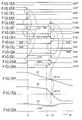
gate 160 is used for triggering the thyristor W2A, an ORed output from ORgate 162 is used for triggering the thyristor U2A, and an ORed output from ORgate 164 is used for triggering the thyristor V2A. An ORed output from ORgate 166 is used for triggering the thyristor WIA, an ORed output from ORgate 168 is used for triggering the thyristor U1A, and an ORed output from ORgate 170 is used for triggering the thyristor VIA. - The trigger control circuit of Fig. 12 in a phase-advanced mode will operate as follows. Figs. 13A to 13R illustrate the timing of signals around time tl in Fig. 4. Around time tl, polyphase signal U2P* has logic "1" level (Fig. 13A). Also, at time tl, the logic level of polyphase signal V1N* is changed from "1" to "0" (Fig. 13B), while the logic level of polyphase signal WIN* is changed from "0" to "1" (Fig. 13C). The leading edge of signal W1N* is differentiated through
differentiation circuit 116, and set pulse E120 corresponding to the differentiated signal edge of WIN* is inputted to RS flip-flop 128 (Fig. 13D). Pulse E120 sets the flip-flop 128 so that the the logic level of Q output E128A becomes "1" (Fig. 13F) and the logic level of inverted Q output E128B becomes "0" (Fig. 13G). - Trigger signal E132 for GTO thyristors GT1 and GT2 of Fig. 9 is generated according to Q output E128A (Fig. 13H). Trigger signal E124 for thyristor X2 of Fig. 8 is obtained at time t11 by delaying the set pulse E120 by given time T through delay circuit 124 (Figs. 13D and 13N).
- Inverted Q output E128B of logic "0" renders the logic level of ORed output E134 to be "0". This logic "0" output E134 is supplied to one input of AND
gate 136. (RS flip-flop 126 is in set-mode in this instant so that the ORed output E134 fromOR gate 134 only depends on the logical level of E128B.) Accordingly, though ANDgate 136 receives at the other input the signal U2P* of logic "1", the ANDed output from ANDgate 136 which is used for triggering the thyristor U2P becomes logic "0" (Fig. 13I). On the other hand, ANDgate 144 receives logic "0" of signal VIN* (Fig. 13B) and logic "0" of ORed output E134. Accordingly, the ANDed output from ANDgate 144 which is used for triggering the thyristor VlN becomes logic "0" (Fig. 13J). - AND
gate 158 receives at its one input the logic "1" of signal WIN* (Fig. 13C) and at the other input the logic "1" of Q output EI28A (Fig. 13F). Then, the ANDed output E158 from ANDgate 158 becomes logic "1". This ANDed output E158 of logic "1" is supplied to ORgates - When the trigger control circuit of Fig. 12 is applied to the embodiment of Fig. 3, triggering signals generated after time tl in Fig. 13 render the thyristors VIA, U2A, Tll and T22 conductive, so that a reverse-charging current path is formed. This reverse-charging current path serves to discharge the capacitor C. Then, the charged voltage VC of capacitor C is lowered (after tl in Fig. 13P). This charged voltage VC is checked in voltage comparator (zero-cross sensor) 130. When the voltage VC reaches 0 volts,
comparator 130 generates the reset pulse E130 (at t12 in Figs. 13E and 13P). Pulse E130 resets flip-flop 128 so that Q output E128A becomes logic "0" (at t12 in Fig. 13F) and inverted Q output E128B becomes logic "1" (at t12 in Fig. 13G). Pulse E130 also resets flip-flop 126 so that E126A and E126B become "0" and "1", respectively. - Q output E128A having logic "0" level is supplied to AND
gate 158 which receives signal WlN* having logic "1" level (at t12 in Figs. 13C and 13F). ANDgate 158 is closed by logic "0" of E128A, so that the ANDed output E158 becomes logic "0". At this time, ANDgates flop 126 which is reset at time t12 by pulse E130. From this, the ANDed outputs respectively supplied from ANDgates gates - At time t12, the logic "0" of Q outputs E126A and E128A renders the logic level of ORed output E132 to "0" (Fig. 13H). At the same-time, the logic "1" of inverted Q outputs E126B and E128B renders the logic level of ORed output E134 to "1". Since AND
gate 136 receives this logic "1" ORed output and signal U2P* having logic level "1" (Fig. 13A), the ANDed output from ANDgate 136 becomes logic "1" (Fig. 131). The above logic "1" ORed output E134 is also supplied to ANDgate 146 which receives signal W1N* having logic level "1" (Fig. 13C). Then, ANDgate 146 provides a logic "1" ANDed output for triggering the thyristor W1N (at t12 in Fig. 13K). The commutation in the phase-advanced mode is thus completed. - The operation of the trigger control circuit of Fig. 12 in a phase-delayed mode is performed according to the timing as illustrated in Fig. 4.
- When the trigger control circuit of Fig. 12 is applied to the embodiment of Fig. 8, triggering signals generated after time tl in Fig. 13 render the thyristors VlA, U2A, Tll and T22 conductive, so that a reverse-charging current path is formed. This reverse-charging current path serves to discharge the capacitor C. Then, the charged voltage VC of capacitor C is lowered (after tl in Fig. 13Q). When a period corresponding to the given delay time T of
delay circuit 124 has elapsed after time tl, trigger signal E124 is generated (time tll in Fig. 13N). Then, thyristor X2 is turned on so that the discharging for capacitor C is accelerated via a current flowing through inductor L and thyristor X2. After time tll, the charged voltage VC is rapidly lowered (Fig. 13Q). This voltage VC is checked in voltage comparator (zero-cross sensor) 130. When the potential of voltage VC crosses the zero potential,comparator 130 generates the reset pulse E130 (at t12 in Figs. 13E and 13Q). Pulse E130 resets flip-flop 128 so that Q output E128A becomes logic "0" and inverted Q output E128B becomes logic "1" (at tl2 in Figs. 13F and 13G). At time t12, ANDed outputs from ANDgates - When the trigger control circuit of Fig. 12 is applied to the embodiment of Fig. 9, triggering signals generated after time tl in Fig. 13 render the thyristors VIA, U2A, GT1 and GT2 conductive, so that a reverse-charging current path is formed. This reverse-charging current path serves to discharge the capacitor C. Then, the charged voltage VC of capacitor C is lowered (after tl in Fig. 13R). This charged voltage VC is checked in
voltage comparator 130. When the potential of voltage VC crosses a reference potential Vref applied to comparator 130 (i.e., VC < Vref),comparator 130 generates the reset pulse E130 (at tl2 in Figs. 13E and 13R). Pulse E130 resets flip-flop 128 so that Q output E128A becomes logic "0" and inverted Q output E128B becomes logic "1" (at t12 in Figs. 13F and 13G). At time t12, ANDed outputs from ANDgates - As has been described above, according to the present invention, reactive power of the power supply can be reduced, and the commutation involves only a moderate current change rate so that substantially no surge voltage is generated. Further, in a certain control angle, an output current from a power transformer becomes zero and power loss in the power transformer is reduced (cf. Fig. 7). Thus, the power conversion efficiency is improved. In addition, as may be seen from some of the embodiments, the power converter of the present invention can be reduced to practice in a relatively simple configuration, in contrast to the advantages obtained.
- Although the present invention has been described with reference to a 3-phase power supply, the present invention may be similarly applied to a single-phase power supply or polyphase power supplies other than 3-phase ones. Fig. 14 shows an example for the single-phase configuration, and Fig. 15 shows an example for the polyphase (4-phase) configuration. Although illustration is omitted, snubber circuits or anode reactors may be adapted to the respective thyristors, or reactors may be provided between each thyristor of the thyristor bridge and the output terminal of the thyristor bridge, thereby reducing mutual interferences among thyristors when commutations are simultaneously performed under the phase-advanced and phase-delayed control modes.
Claims (12)
and characterized in that said trigger control means (Fig. 12) includes means (130, 126, 128, 134-170) coupled to said capacitor (C), said first to fourth thyristors (Tll, T12, T21, T22), said first auxiliary thyristors (U1A, VIA, WlA) and said second auxiliary thyristors (U2A, V2A, W2A), for comparing a capacitor voltage (VC) appearing across said capacitor (C) with a given voltage (zero volts) and enabling the commutation of said commutation circuit means (18, 33) when the capacitor voltage (VC) corresponds to the given voltage (at tl2 in Figs. 13P and 13Q).
and characterized in that said trigger control means (Fig. 12) includes means (130, 126, 128, 132-170) coupled to said capacitor (C), said first and second gate turn-off thyristors (GT1, GT2), said first auxiliary thyristors (U1A, VIA, W1A) and said second auxiliary thyristors (U2A, V2A, W2A), for comparing a capacitor voltage (VC) appearing across said capacitor (C) with a reference voltage (Vref) and enabling the commutation of said commutation circuit means (34) when the capacitor voltage (VC) corresponds to the reference voltage (at tl2 in Fig. 13R).
Applications Claiming Priority (2)
| Application Number | Priority Date | Filing Date | Title |
|---|---|---|---|
| JP96129/83 | 1983-05-31 | ||
| JP58096129A JPS59222079A (en) | 1983-05-31 | 1983-05-31 | Power converter |
Publications (3)
| Publication Number | Publication Date |
|---|---|
| EP0127187A2 true EP0127187A2 (en) | 1984-12-05 |
| EP0127187A3 EP0127187A3 (en) | 1986-03-19 |
| EP0127187B1 EP0127187B1 (en) | 1988-11-09 |
Family
ID=14156772
Family Applications (1)
| Application Number | Title | Priority Date | Filing Date |
|---|---|---|---|
| EP84106203A Expired EP0127187B1 (en) | 1983-05-31 | 1984-05-30 | Power converter |
Country Status (4)
| Country | Link |
|---|---|
| US (1) | US4555752A (en) |
| EP (1) | EP0127187B1 (en) |
| JP (1) | JPS59222079A (en) |
| DE (1) | DE3475150D1 (en) |
Cited By (1)
| Publication number | Priority date | Publication date | Assignee | Title |
|---|---|---|---|---|
| EP2950432A1 (en) * | 2014-05-28 | 2015-12-02 | ABB Technology Ltd | Rectifier with controllable power factor and method for controlling the rectifier |
Families Citing this family (7)
| Publication number | Priority date | Publication date | Assignee | Title |
|---|---|---|---|---|
| JPH0740761B2 (en) * | 1985-04-19 | 1995-05-01 | 株式会社日立製作所 | AC electric vehicle control device |
| JP2533513B2 (en) * | 1987-02-06 | 1996-09-11 | 株式会社日立製作所 | Control device for converter circuit |
| US6329726B1 (en) * | 2000-03-03 | 2001-12-11 | Broadband Telcom Power, Inc. | Proportional distribution of power from a plurality of power sources |
| US6177781B1 (en) * | 2000-05-25 | 2001-01-23 | Steve Yiua Shi Yin | Power-factor improvement device |
| JPWO2007069314A1 (en) * | 2005-12-14 | 2009-05-21 | 東芝三菱電機産業システム株式会社 | Power converter |
| TW201218049A (en) * | 2010-10-19 | 2012-05-01 | xiang-yu Li | employing measurement of electric field variation to identify touch control input |
| FR3068547B1 (en) * | 2017-06-30 | 2019-08-16 | Stmicroelectronics (Tours) Sas | THYRISTORS REVERSIBLE AC / DC CONVERTER |
Citations (3)
| Publication number | Priority date | Publication date | Assignee | Title |
|---|---|---|---|---|
| JPS55109172A (en) * | 1979-02-10 | 1980-08-22 | Toshiba Corp | Power converter |
| JPS5641770A (en) * | 1979-09-11 | 1981-04-18 | Toshiba Corp | Power converter |
| JPS5683267A (en) * | 1979-12-08 | 1981-07-07 | Fuji Electric Co Ltd | Power conversion system |
Family Cites Families (4)
| Publication number | Priority date | Publication date | Assignee | Title |
|---|---|---|---|---|
| JPS5820014B2 (en) * | 1975-06-27 | 1983-04-21 | キヤノン株式会社 | Senzou Keiseiko Gakusouchi |
| JPS5312030A (en) * | 1976-07-21 | 1978-02-03 | Fuji Electric Co Ltd | Power converter |
| JPS6013204B2 (en) * | 1978-02-27 | 1985-04-05 | 株式会社東芝 | power converter |
| JPS54115688A (en) * | 1978-02-28 | 1979-09-08 | Toyota Motor Corp | Reference oxygen producing composition for oxygen sensor |
-
1983
- 1983-05-31 JP JP58096129A patent/JPS59222079A/en active Pending
-
1984
- 1984-05-24 US US06/613,730 patent/US4555752A/en not_active Expired - Fee Related
- 1984-05-30 EP EP84106203A patent/EP0127187B1/en not_active Expired
- 1984-05-30 DE DE8484106203T patent/DE3475150D1/en not_active Expired
Patent Citations (3)
| Publication number | Priority date | Publication date | Assignee | Title |
|---|---|---|---|---|
| JPS55109172A (en) * | 1979-02-10 | 1980-08-22 | Toshiba Corp | Power converter |
| JPS5641770A (en) * | 1979-09-11 | 1981-04-18 | Toshiba Corp | Power converter |
| JPS5683267A (en) * | 1979-12-08 | 1981-07-07 | Fuji Electric Co Ltd | Power conversion system |
Non-Patent Citations (3)
| Title |
|---|
| PATENT ABSTRACTS OF JAPAN, vol. 4, no. 162 (E-33)[644], 12th November 1980; & JP-A-55 109 172 (TOKYO SHIBAURA DENKI K.K.) 22-08-1980 * |
| PATENT ABSTRACTS OF JAPAN, vol. 5, no. 149 (E-75)[821], 19th September 1981; & JP-A-56 083 267 (FUJI DENKI SEIZO K.K.) 07-07-1981 * |
| PATENT ABSTRACTS OF JAPAN, vol. 5, no. 99 (E-63)[771], 26th June 1981; & JP-A-56 041 770 (TOKYO SHIBAURA DENKI K.K.) 18-04-1981 * |
Cited By (1)
| Publication number | Priority date | Publication date | Assignee | Title |
|---|---|---|---|---|
| EP2950432A1 (en) * | 2014-05-28 | 2015-12-02 | ABB Technology Ltd | Rectifier with controllable power factor and method for controlling the rectifier |
Also Published As
| Publication number | Publication date |
|---|---|
| DE3475150D1 (en) | 1988-12-15 |
| EP0127187A3 (en) | 1986-03-19 |
| JPS59222079A (en) | 1984-12-13 |
| US4555752A (en) | 1985-11-26 |
| EP0127187B1 (en) | 1988-11-09 |
Similar Documents
| Publication | Publication Date | Title |
|---|---|---|
| US6937483B2 (en) | Device and method of commutation control for an isolated boost converter | |
| US5926381A (en) | DC power supply apparatus | |
| US5930122A (en) | Inverter and DC power supply apparatus with inverter used therein | |
| US4926306A (en) | Electric power converter | |
| Fujiwara et al. | A novel lossless passive snubber for soft-switching boost-type converters | |
| JPS6160667B2 (en) | ||
| US4514795A (en) | High-voltage generator, notably for an X-ray tube | |
| EP0127187B1 (en) | Power converter | |
| US4710862A (en) | Inverter | |
| US3372326A (en) | High efficiency low iron ac-to-regulated dc converter | |
| US4855887A (en) | Current and frequency converter having means to reduce switching losses | |
| KR830001639B1 (en) | Selective Current Circuit for Inverter | |
| JP2720001B2 (en) | DC-DC converter | |
| US4455600A (en) | Single phase, double-ended thyristor inverter with choke-coupled impulse commutation | |
| JP2618931B2 (en) | Power converter | |
| JPH0685632B2 (en) | DC / DC converter | |
| JPS6215023B2 (en) | ||
| SU1432684A1 (en) | Arrangement for switching rectifiers of transformer-gate converter | |
| JPH05115178A (en) | Power converter | |
| JPH07107743A (en) | Converter device | |
| JPH0336221Y2 (en) | ||
| JPS5932233Y2 (en) | Current source inverter device | |
| SU760303A1 (en) | Storage battery charging device | |
| JPH04255470A (en) | Rectifying circuit | |
| JPH01120912A (en) | Gate circuit of gate turn-off thyristor |
Legal Events
| Date | Code | Title | Description |
|---|---|---|---|
| PUAI | Public reference made under article 153(3) epc to a published international application that has entered the european phase |
Free format text: ORIGINAL CODE: 0009012 |
|
| 17P | Request for examination filed |
Effective date: 19840530 |
|
| AK | Designated contracting states |
Designated state(s): CH DE FR GB LI SE |
|
| PUAL | Search report despatched |
Free format text: ORIGINAL CODE: 0009013 |
|
| AK | Designated contracting states |
Kind code of ref document: A3 Designated state(s): CH DE FR GB LI SE |
|
| 17Q | First examination report despatched |
Effective date: 19870909 |
|
| GRAA | (expected) grant |
Free format text: ORIGINAL CODE: 0009210 |
|
| AK | Designated contracting states |
Kind code of ref document: B1 Designated state(s): CH DE FR GB LI SE |
|
| REF | Corresponds to: |
Ref document number: 3475150 Country of ref document: DE Date of ref document: 19881215 |
|
| ET | Fr: translation filed | ||
| PLBE | No opposition filed within time limit |
Free format text: ORIGINAL CODE: 0009261 |
|
| STAA | Information on the status of an ep patent application or granted ep patent |
Free format text: STATUS: NO OPPOSITION FILED WITHIN TIME LIMIT |
|
| 26N | No opposition filed | ||
| PGFP | Annual fee paid to national office [announced via postgrant information from national office to epo] |
Ref country code: GB Payment date: 19920505 Year of fee payment: 9 |
|
| PGFP | Annual fee paid to national office [announced via postgrant information from national office to epo] |
Ref country code: FR Payment date: 19920511 Year of fee payment: 9 |
|
| PGFP | Annual fee paid to national office [announced via postgrant information from national office to epo] |
Ref country code: SE Payment date: 19920521 Year of fee payment: 9 |
|
| PGFP | Annual fee paid to national office [announced via postgrant information from national office to epo] |
Ref country code: CH Payment date: 19920525 Year of fee payment: 9 |
|
| PGFP | Annual fee paid to national office [announced via postgrant information from national office to epo] |
Ref country code: DE Payment date: 19920610 Year of fee payment: 9 |
|
| PG25 | Lapsed in a contracting state [announced via postgrant information from national office to epo] |
Ref country code: GB Effective date: 19930530 |
|
| PG25 | Lapsed in a contracting state [announced via postgrant information from national office to epo] |
Ref country code: SE Effective date: 19930531 Ref country code: LI Effective date: 19930531 Ref country code: CH Effective date: 19930531 |
|
| GBPC | Gb: european patent ceased through non-payment of renewal fee |
Effective date: 19930530 |
|
| PG25 | Lapsed in a contracting state [announced via postgrant information from national office to epo] |
Ref country code: FR Effective date: 19940131 |
|
| REG | Reference to a national code |
Ref country code: CH Ref legal event code: PL |
|
| PG25 | Lapsed in a contracting state [announced via postgrant information from national office to epo] |
Ref country code: DE Effective date: 19940201 |
|
| REG | Reference to a national code |
Ref country code: FR Ref legal event code: ST |
|
| EUG | Se: european patent has lapsed |
Ref document number: 84106203.7 Effective date: 19931210 |