EP0126417A2 - Détecteur d'images par rayonnement et méthode pour détecter de telles images avec ce détecteur - Google Patents
Détecteur d'images par rayonnement et méthode pour détecter de telles images avec ce détecteur Download PDFInfo
- Publication number
- EP0126417A2 EP0126417A2 EP84105523A EP84105523A EP0126417A2 EP 0126417 A2 EP0126417 A2 EP 0126417A2 EP 84105523 A EP84105523 A EP 84105523A EP 84105523 A EP84105523 A EP 84105523A EP 0126417 A2 EP0126417 A2 EP 0126417A2
- Authority
- EP
- European Patent Office
- Prior art keywords
- radiation image
- phosphor layer
- phosphor
- image detector
- radiation
- Prior art date
- Legal status (The legal status is an assumption and is not a legal conclusion. Google has not performed a legal analysis and makes no representation as to the accuracy of the status listed.)
- Ceased
Links
- 230000005855 radiation Effects 0.000 title claims abstract description 81
- 238000000034 method Methods 0.000 title claims abstract description 31
- OAICVXFJPJFONN-UHFFFAOYSA-N Phosphorus Chemical compound [P] OAICVXFJPJFONN-UHFFFAOYSA-N 0.000 claims abstract description 67
- 229910052761 rare earth metal Inorganic materials 0.000 claims description 6
- 229910052771 Terbium Inorganic materials 0.000 claims description 5
- GZCRRIHWUXGPOV-UHFFFAOYSA-N terbium atom Chemical compound [Tb] GZCRRIHWUXGPOV-UHFFFAOYSA-N 0.000 claims description 5
- 229910052693 Europium Inorganic materials 0.000 claims description 4
- 229910052784 alkaline earth metal Inorganic materials 0.000 claims description 4
- 150000001342 alkaline earth metals Chemical class 0.000 claims description 4
- OGPBJKLSAFTDLK-UHFFFAOYSA-N europium atom Chemical compound [Eu] OGPBJKLSAFTDLK-UHFFFAOYSA-N 0.000 claims description 4
- 150000002910 rare earth metals Chemical class 0.000 claims description 4
- UAHZTKVCYHJBJQ-UHFFFAOYSA-N [P].S=O Chemical compound [P].S=O UAHZTKVCYHJBJQ-UHFFFAOYSA-N 0.000 claims 2
- 239000000463 material Substances 0.000 description 13
- 239000011230 binding agent Substances 0.000 description 10
- 239000011248 coating agent Substances 0.000 description 10
- 238000000576 coating method Methods 0.000 description 10
- 229910021417 amorphous silicon Inorganic materials 0.000 description 8
- 239000006185 dispersion Substances 0.000 description 8
- 239000002245 particle Substances 0.000 description 8
- TZCXTZWJZNENPQ-UHFFFAOYSA-L barium sulfate Chemical compound [Ba+2].[O-]S([O-])(=O)=O TZCXTZWJZNENPQ-UHFFFAOYSA-L 0.000 description 6
- 238000010586 diagram Methods 0.000 description 6
- 229910052751 metal Inorganic materials 0.000 description 6
- 239000002184 metal Substances 0.000 description 6
- 230000035945 sensitivity Effects 0.000 description 5
- 229910052775 Thulium Inorganic materials 0.000 description 4
- -1 rare earth oxysulfide Chemical class 0.000 description 4
- VYPSYNLAJGMNEJ-UHFFFAOYSA-N Silicium dioxide Chemical compound O=[Si]=O VYPSYNLAJGMNEJ-UHFFFAOYSA-N 0.000 description 3
- 229910052782 aluminium Inorganic materials 0.000 description 3
- XAGFODPZIPBFFR-UHFFFAOYSA-N aluminium Chemical compound [Al] XAGFODPZIPBFFR-UHFFFAOYSA-N 0.000 description 3
- WDIHJSXYQDMJHN-UHFFFAOYSA-L barium chloride Chemical compound [Cl-].[Cl-].[Ba+2] WDIHJSXYQDMJHN-UHFFFAOYSA-L 0.000 description 3
- 229910001626 barium chloride Inorganic materials 0.000 description 3
- 229910052793 cadmium Inorganic materials 0.000 description 3
- 238000001514 detection method Methods 0.000 description 3
- 238000003384 imaging method Methods 0.000 description 3
- 230000001681 protective effect Effects 0.000 description 3
- 238000002601 radiography Methods 0.000 description 3
- 239000004065 semiconductor Substances 0.000 description 3
- RTZKZFJDLAIYFH-UHFFFAOYSA-N Diethyl ether Chemical compound CCOCC RTZKZFJDLAIYFH-UHFFFAOYSA-N 0.000 description 2
- 229910052688 Gadolinium Inorganic materials 0.000 description 2
- 239000000020 Nitrocellulose Substances 0.000 description 2
- 229920002433 Vinyl chloride-vinyl acetate copolymer Polymers 0.000 description 2
- 229910001632 barium fluoride Inorganic materials 0.000 description 2
- 238000007796 conventional method Methods 0.000 description 2
- 239000011521 glass Substances 0.000 description 2
- 229910044991 metal oxide Inorganic materials 0.000 description 2
- 150000004706 metal oxides Chemical class 0.000 description 2
- 238000002156 mixing Methods 0.000 description 2
- 229920001220 nitrocellulos Polymers 0.000 description 2
- 229920003229 poly(methyl methacrylate) Polymers 0.000 description 2
- 229920002037 poly(vinyl butyral) polymer Polymers 0.000 description 2
- 239000004926 polymethyl methacrylate Substances 0.000 description 2
- 229920002689 polyvinyl acetate Polymers 0.000 description 2
- 239000011118 polyvinyl acetate Substances 0.000 description 2
- 229920001059 synthetic polymer Polymers 0.000 description 2
- XOLBLPGZBRYERU-UHFFFAOYSA-N tin dioxide Chemical compound O=[Sn]=O XOLBLPGZBRYERU-UHFFFAOYSA-N 0.000 description 2
- 238000012935 Averaging Methods 0.000 description 1
- 229910004829 CaWO4 Inorganic materials 0.000 description 1
- 229920002307 Dextran Polymers 0.000 description 1
- LFQSCWFLJHTTHZ-UHFFFAOYSA-N Ethanol Chemical compound CCO LFQSCWFLJHTTHZ-UHFFFAOYSA-N 0.000 description 1
- 239000001856 Ethyl cellulose Substances 0.000 description 1
- ZZSNKZQZMQGXPY-UHFFFAOYSA-N Ethyl cellulose Chemical compound CCOCC1OC(OC)C(OCC)C(OCC)C1OC1C(O)C(O)C(OC)C(CO)O1 ZZSNKZQZMQGXPY-UHFFFAOYSA-N 0.000 description 1
- 108010010803 Gelatin Proteins 0.000 description 1
- 229920000084 Gum arabic Polymers 0.000 description 1
- 229910002420 LaOCl Inorganic materials 0.000 description 1
- 229910001477 LaPO4 Inorganic materials 0.000 description 1
- 229910017672 MgWO4 Inorganic materials 0.000 description 1
- 229910019142 PO4 Inorganic materials 0.000 description 1
- 239000004952 Polyamide Substances 0.000 description 1
- 239000004698 Polyethylene Substances 0.000 description 1
- 239000004372 Polyvinyl alcohol Substances 0.000 description 1
- 229920001328 Polyvinylidene chloride Polymers 0.000 description 1
- 241000978776 Senegalia senegal Species 0.000 description 1
- UCKMPCXJQFINFW-UHFFFAOYSA-N Sulphide Chemical compound [S-2] UCKMPCXJQFINFW-UHFFFAOYSA-N 0.000 description 1
- 229920001986 Vinylidene chloride-vinyl chloride copolymer Polymers 0.000 description 1
- FJWGYAHXMCUOOM-QHOUIDNNSA-N [(2s,3r,4s,5r,6r)-2-[(2r,3r,4s,5r,6s)-4,5-dinitrooxy-2-(nitrooxymethyl)-6-[(2r,3r,4s,5r,6s)-4,5,6-trinitrooxy-2-(nitrooxymethyl)oxan-3-yl]oxyoxan-3-yl]oxy-3,5-dinitrooxy-6-(nitrooxymethyl)oxan-4-yl] nitrate Chemical compound O([C@@H]1O[C@@H]([C@H]([C@H](O[N+]([O-])=O)[C@H]1O[N+]([O-])=O)O[C@H]1[C@@H]([C@@H](O[N+]([O-])=O)[C@H](O[N+]([O-])=O)[C@@H](CO[N+]([O-])=O)O1)O[N+]([O-])=O)CO[N+](=O)[O-])[C@@H]1[C@@H](CO[N+]([O-])=O)O[C@@H](O[N+]([O-])=O)[C@H](O[N+]([O-])=O)[C@H]1O[N+]([O-])=O FJWGYAHXMCUOOM-QHOUIDNNSA-N 0.000 description 1
- 238000010521 absorption reaction Methods 0.000 description 1
- 239000000205 acacia gum Substances 0.000 description 1
- 235000010489 acacia gum Nutrition 0.000 description 1
- 239000000654 additive Substances 0.000 description 1
- 239000000853 adhesive Substances 0.000 description 1
- 230000002411 adverse Effects 0.000 description 1
- 230000015572 biosynthetic process Effects 0.000 description 1
- 229920002678 cellulose Polymers 0.000 description 1
- 239000001913 cellulose Substances 0.000 description 1
- 229920002301 cellulose acetate Polymers 0.000 description 1
- 229920006217 cellulose acetate butyrate Polymers 0.000 description 1
- 238000006243 chemical reaction Methods 0.000 description 1
- 238000000151 deposition Methods 0.000 description 1
- 230000008021 deposition Effects 0.000 description 1
- 230000006866 deterioration Effects 0.000 description 1
- 238000003745 diagnosis Methods 0.000 description 1
- 239000002270 dispersing agent Substances 0.000 description 1
- 238000001035 drying Methods 0.000 description 1
- 230000000694 effects Effects 0.000 description 1
- 150000002148 esters Chemical class 0.000 description 1
- 235000019325 ethyl cellulose Nutrition 0.000 description 1
- 229920001249 ethyl cellulose Polymers 0.000 description 1
- 230000005669 field effect Effects 0.000 description 1
- 229920000159 gelatin Polymers 0.000 description 1
- 239000008273 gelatin Substances 0.000 description 1
- 235000019322 gelatine Nutrition 0.000 description 1
- 235000011852 gelatine desserts Nutrition 0.000 description 1
- 150000004676 glycans Chemical class 0.000 description 1
- YPDKFMYSITXPDU-UHFFFAOYSA-B hafnium(4+) tetraphosphate Chemical compound [Hf+4].[Hf+4].[Hf+4].[O-]P([O-])([O-])=O.[O-]P([O-])([O-])=O.[O-]P([O-])([O-])=O.[O-]P([O-])([O-])=O YPDKFMYSITXPDU-UHFFFAOYSA-B 0.000 description 1
- XMBWDFGMSWQBCA-UHFFFAOYSA-N hydrogen iodide Chemical compound I XMBWDFGMSWQBCA-UHFFFAOYSA-N 0.000 description 1
- 238000007689 inspection Methods 0.000 description 1
- 239000011810 insulating material Substances 0.000 description 1
- 150000002576 ketones Chemical class 0.000 description 1
- 230000031700 light absorption Effects 0.000 description 1
- 229920005615 natural polymer Polymers 0.000 description 1
- 239000010452 phosphate Substances 0.000 description 1
- 239000002985 plastic film Substances 0.000 description 1
- 239000004014 plasticizer Substances 0.000 description 1
- 229920002647 polyamide Polymers 0.000 description 1
- 229920000515 polycarbonate Polymers 0.000 description 1
- 239000004417 polycarbonate Substances 0.000 description 1
- 229920000728 polyester Polymers 0.000 description 1
- 229920000573 polyethylene Polymers 0.000 description 1
- 229920000139 polyethylene terephthalate Polymers 0.000 description 1
- 239000005020 polyethylene terephthalate Substances 0.000 description 1
- 229920001282 polysaccharide Polymers 0.000 description 1
- 239000005017 polysaccharide Substances 0.000 description 1
- 239000004814 polyurethane Substances 0.000 description 1
- 229920002635 polyurethane Polymers 0.000 description 1
- 229920002451 polyvinyl alcohol Polymers 0.000 description 1
- 239000005033 polyvinylidene chloride Substances 0.000 description 1
- 238000003825 pressing Methods 0.000 description 1
- 108090000623 proteins and genes Proteins 0.000 description 1
- 102000004169 proteins and genes Human genes 0.000 description 1
- 230000035939 shock Effects 0.000 description 1
- 239000000377 silicon dioxide Substances 0.000 description 1
- 235000012239 silicon dioxide Nutrition 0.000 description 1
- 239000002904 solvent Substances 0.000 description 1
- 230000002269 spontaneous effect Effects 0.000 description 1
- 229910052712 strontium Inorganic materials 0.000 description 1
- 239000000126 substance Substances 0.000 description 1
- FRNOGLGSGLTDKL-UHFFFAOYSA-N thulium atom Chemical compound [Tm] FRNOGLGSGLTDKL-UHFFFAOYSA-N 0.000 description 1
- 229910001887 tin oxide Inorganic materials 0.000 description 1
- PBYZMCDFOULPGH-UHFFFAOYSA-N tungstate Chemical compound [O-][W]([O-])(=O)=O PBYZMCDFOULPGH-UHFFFAOYSA-N 0.000 description 1
- 238000001771 vacuum deposition Methods 0.000 description 1
- 229920002554 vinyl polymer Polymers 0.000 description 1
- 229910000164 yttrium(III) phosphate Inorganic materials 0.000 description 1
Images

Classifications
-
- H—ELECTRICITY
- H01—ELECTRIC ELEMENTS
- H01L—SEMICONDUCTOR DEVICES NOT COVERED BY CLASS H10
- H01L31/00—Semiconductor devices sensitive to infrared radiation, light, electromagnetic radiation of shorter wavelength or corpuscular radiation and specially adapted either for the conversion of the energy of such radiation into electrical energy or for the control of electrical energy by such radiation; Processes or apparatus specially adapted for the manufacture or treatment thereof or of parts thereof; Details thereof
- H01L31/02—Details
- H01L31/0232—Optical elements or arrangements associated with the device
- H01L31/02322—Optical elements or arrangements associated with the device comprising luminescent members, e.g. fluorescent sheets upon the device
Definitions
- the present invention relates to a radiation image detector and a method for detecting radiation image using said detector. More particularly, the present invention relates to a radiation image detector which employs the combination of a phosphor and photosensitive elements, and a method for detecting radiation image using said detector.
- the so-called radiographic method using a combination of a radiographic intensifying screen and a radiographic film is generally utilized as a method for obtaining a radiation image of an object.
- a radiation such as X-rays having passed through an object impinges upon a radiographic intensifying screen
- a phosphor contained in the intensifying screen absorbs the radiation energy and emits light (spontaneous emission).
- a radiographic film provided in close contact with the radiographic int.ensi- fying screen is exposed to the light emitted by the screen to form a radiation image of the object on the film.
- the radiation image is directly obtained as a visible image on the radiographic film.
- the image information is photoelectrically read out in such a manner that the visible image on the radiographic film is scanned with a light beam to convert the image into an electric signal, and then the electric signal is subjected to a suitable image processing to reproduce an image meeting the purpose.
- the conventional radiographic method has been utilized widely in the variety of radiography. It is accordingly desired that the sensitivity of the radiographic method and the quality of an image (sharpness and graininess, etc.) provided thereby are made as high as possible.
- the present inventors have studied to solve the above-mentioned problems in the conventional radiographic method, and found that these problems are solved or reduced by directly obtaining image information on a radiation image of an object as an electric signal by means of a radiation image detector, which comprises a photosensitive member composed of numerous photosensitive elements in regular and two-dimensional arrangement and a phosphor layer provided thereon.
- the present invention provides a radiation image detector which comprises:
- the present invention provides a method for detecting radiation image which comprises steps of:
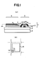
- Figures 1-(a) and 1-(b) are a schematic partial section view and partial illustrative diagram which show the embodiment of the radiation image detector of the present invention, respectively.
- Figure 2 is a schematic circuit diagram which shows the embodiment of the radiation image detector of the present invention.
- the radiation image (i.e., transmitted radiation image) of an object can be directly obtained as an electric signal using the radiation image detector which comprises a phosphor layer and a photosensitive member comprising numerous photosensitive elements, by causing the phosphor of the phosphor layer to absorb a radiation such as X-rays which has impinged upon the phosphor layer after passing through the object and to emit light immediately, and then causing the light detecting menber to receive the emitted light and to convert it into an electric signal.
- the radiation image detector which comprises a phosphor layer and a photosensitive member comprising numerous photosensitive elements
- the present invention it is possible to reproduce an image from the obtained electric signal having the radiation image information with a desired means such as display on CRT, etc. or record on a heatsensitive recording material, as well as to visualize an image on a photosensitive film in the conventional manner.
- the radiation image information can be also recorded and stored in another form by using a magnetic tape or the like.
- the image information which is hardly affected by these factors can be obtained by amplifying the electric signal suitably. That is, according to the present invention, the radiation dose applied to the object can be reduced by adjusting the output of the electric signal, as compared with the conventional method, so that this method is especially useful in the case of the object being a human body.
- the obtained electric signal may be subjected to the suitable image processing in the present invention, if desired, to give a visualized image with an excellent readability.
- the photosensitive material necessarily employed to give an image in the conventional radiographic method, such as a radiographic film, is not required, and the requirement that the sensitivity region of the photosensitive material overlaps with that of the radiographic intensifying screen used therewith is eliminated.
- the radiation image detector according to the present invention basically comprises a photosensitive member comprising numerous photosensitive elements in regular and two-dimensional arrangement, and a phosphor layer provided thereon.
- a photosensitive element employed in the photosensitive member comprises a light receiving section to receive the light emitted by the phosphor layer and a transferring section to sequentially output an electric charge obtained through the photoelectrical conversion at the light receiving section as an electric signal.
- a known solid-state imaging . device using an amorphous semiconductor or the like can be employed as the photosensitive element.
- solid-state imaging device examples include sensors such as MOS (Metal Oxide Semiconductor), CCD (Charged Coupled Device), BBD (Bucket Brigade Device), and CID (Charged Isolated Device).
- sensors such as MOS (Metal Oxide Semiconductor), CCD (Charged Coupled Device), BBD (Bucket Brigade Device), and CID (Charged Isolated Device).
- photoconductive material employed for the solid-state imaging devices include amorphous silicon (a-Si), ZnO, and CdS.
- the photosensitive member is provided with an insulating layer, and a phosphor layer is provided on the insulating layer.
- a phosphor layer is provided on the insulating layer.
- the material of the insulating layer include light-transmissive insulating materials such as glass and transparent polymeric material.
- the phosphor layer usually comprises a binder and phosphor particles dispersed therein.
- a variety of phosphors employable for a radiographic intensifying screen in the conventional radiographic method can be employed in the present invention.
- Examples of the phosphor preferably employable in the invention include:
- phosphors are given by no means to restrict the phosphor employable in the present invention. Any other phosphors can also be employed, provided that the phosphor emits light having a wavelength within near ultraviolet to visible region when exposed to a radiation such as X-rays.
- the phosphor employed in the present invention that the wavelength region of light emission thereof overlaps with the wavelength region of light absorption of the photoconductive material employed in the light receiving section of photosensitive element. More in detail, it is required in the present invention to select such a phosphor and photoconductive material that at least a part of the wavelength region of emission of the former coincides with at least a part of the wavelength region of absorption of the latter.
- a phosphor having an emission wavelength of near 600 nm is preferably employed in combination therewith.
- ZnS and CdS are preferably employed as the photoconductive material.
- binder to be contained in the phosphor layer examples include: natural polymers such as proteins (e.g. gelatin), polysaccharides (e.g. dextran) and gum arabic; and synthetic polymers such as polyvinyl butyral, polyvinyl acetate, nitrocellulose, ethylcellulose, vinylidene chloride-vinyl chloride copolymer, polymethyl methacrylate, vinyl chloride-vinyl acetate copolymer, polyurethane, cellulose acetate butyrate, polyvinyl alcohol, and linear polyester.
- natural polymers such as proteins (e.g. gelatin), polysaccharides (e.g. dextran) and gum arabic
- synthetic polymers such as polyvinyl butyral, polyvinyl acetate, nitrocellulose, ethylcellulose, vinylidene chloride-vinyl chloride copolymer, polymethyl methacrylate, vinyl chloride-vinyl acetate copolymer, polyurethane
- the phosphor layer can be formed on the insulating layer, for instance, by the following procedure.
- phosphor particles and a binder are added to an appropriate solvent such as lower alcohol, ketone, ester, or ether, and then they are mixed to prepare a coating dispersion of the phosphor particles in the binder solution.
- an appropriate solvent such as lower alcohol, ketone, ester, or ether
- the mixing ratio between the binder and the phosphor in the coating dispersion varies depending on the characteristics of the radiation image detector to be obtained, type of the photosensitive element employed, and nature 3 f the phosphor employed, but in general the mixing ratio therebetween is within the range of from 1 : 1 to 1 : 100 (binder : phosphor, by weight), and in particular preferably from 1 : 8 to 1 : 40.
- the coating dispersion may contain a variety of additives such as a dispersing agent for increasing the dispersibility of the phosphor particles therein and a plasticizer for increasing the bonding strength between the binder and phosphor particles in the phosphor layer after forming a layer.
- additives such as a dispersing agent for increasing the dispersibility of the phosphor particles therein and a plasticizer for increasing the bonding strength between the binder and phosphor particles in the phosphor layer after forming a layer.
- the coating dispersion containing the phosphor particles and the binder prepared as described above is applied evenly onto the surface of the insulating layer to form a layer of the coating dispersion.
- the coating procedure can be carried out by a conventional method such as a method using a doctor blade, a roll coater, or knife coater.
- the coating dispersion After applying the coating dispersion to the insulating layer, the coating dispersion is then heated slowly to dryness so as to complete the formation of a phosphor layer.
- the thickness of the phosphor layer varies depending upon the characteristics of the aimed radiation image detector, nature of the phosphor, and the ratio between the binder and the phosphor, etc. Generally, the thickness of the phosphor layer is within a range of from 20 ⁇ m to 1 mm, and preferably from 50 to 500 ⁇ m.
- the phosphor layer is initially prepared on a sheet such as a metal plate, glass plate, or a plastic sheet by coating the coating dispersion thereon and drying it, and thus prepared phosphor layer is then laminated on the insulating layer by pressing or using an adhesive agent.
- the phosphor layer can be formed with no binder.
- the phosphor layer can be formed on the insulating layer by deposition of the phosphor particles thereon such as vacuum deposition.
- a transparent protective film is preferably provided on the phosphor layer to protect the phosphor layer from physical shocks and chemical deterioration.
- the protective film can be made of a cellulose derivative such as cellulose acetate or nitrocellulose; or a synthetic polymer such as polymethyl methacrylate, polyvinyl butyral, polyvinyl formal, polycarbonate, polyvinyl acetate, vinyl chloride-vinyl acetate copolymer, polyethylene terephthalate, polyethylene, polyvinylidene chloride or polyamide.
- the protective film preferably has a thickness within the range of approximately 3 to 20 ⁇ m.
- Figure 1-(a) shows a vertical section view of one pixel of the radiation image detector comprising a photosensitive member and a phosphor layer provided thereon.
- the radiation image detector is composed of a photosensitive element 1, an insulating layer 2 and a phosphor layer 3, superposed in this order.
- the photodiode 4 comprises a metal layer 6 of aluminum, etc., which serves as an earth, a p-type a-Si:H layer 7, an i-type a-Si:H layer 8, and a transparent electrode layer 9 of tin oxide (Sn0 2 ), superposed in this order.
- the MOS:FET 5 comprises metal layers 10 and 11 of aluminum, etc., which are provided on both sides of an a-Si:H layer 12, the a-Si:H layer 12, an insulating layer 13 of silicon dioxide (Si0 2 ), and a transferring electrode 14 of aluminum, etc., provided in this order.
- the metal layer 11 serves as a drain and is connected to a transferring resistor.
- the transferring electrode 14 serves as a gate and is connected to a scanning pulse generator.
- Figure 1-(b) shows a schematic illustrative diagram including wiring of a photosensitive element (i.e., a pixel) corresponding to Figure 1-(a).
- the photosensitive element comprises a light receiving section 15 and a transferring section 16, said transferring section being connected to the transferring resistor and scanning pulse generator.
- the area of the light receiving section is preferably as large as possible.
- the embodiment shown in Figure 1-(a) is given by no means to restrict the radiation image detector of the present invention.
- FIG 2 is a schematic circuit diagram of the photosensitive member of the radiation image detector of the present invention.
- One pixel 21 corresponds to the element of Figures 1-(a) and 1-(b), and consists of a light receiving section 22 and a transferring section 23.
- Each transferring section in the photosensitive member is connected to a scanning pulse generator 24 and a transferring resistor 25, individually.
- an output terminal 26 is provided on the transferring resistor 25, an output terminal 26 is provided.
- an object is placed between a radiation generator and the radiation image detector, and a radiation having been generated by the generator and passed through the object impinges upon the phosphor layer-side surface of the radiation image detector: that is, the radiation having the intensity corresponding to the transmitted radiation image of the object impinges upon the lower side of Figure 1-(a).
- the phosphor particles in the phosphor layer 3 absorbs the radiation and immediately emit light.
- the emitted light is received by the photodiode 4 in the photosensitive element 1 which constitutes a photosensitive member, and a signal charge corresponding to the light is produced in the photodiode 4.
- the signal charges are produced in every photosensitive element of the radiation image detector, the signal charge being proportional to the luminance of the emission, namely the intensity of the applied radiation.
- each of the transferring section on the top row turns to a switch-on state (in Figure 1-(a), such a state that a given voltage is applied to the transferring electrode 14 and an electric current passes from the metal layer 10 to the metal layer 11).
- a switch-on state in Figure 1-(a)
- the signal charge generated in the photodiode 4 in Figure 1-(a) is transferred via the MOS:FET 5. Consequently, a signal charge of each photosensitive element in the top row is simultaneously transferred to the transferring resistor 25, and an electric signal corresponding to each photosensitive element is output from the output terminal 26 of the transferring resistor 25.
- the transferring pulse generated by the scanning pulse generator 24 is transferred to each row in the order of from the top to bottom row, and the electric signal produced in each photosensitive element of each row is sequentially output from the output terminal 26.
- the output electric signal is amplified in an amplifier and reproduced as an image in an image reproducing apparatus.
- the obtained electric signal may be subjected to the image processing such as spatial frequency processing, gradiation processing, addition averaging processing, reduction processing and enlarging processing, if desired.
- reproduced image can be recorded on a recording medium, or displayed on a displaying device.
- the recording medium include a medium for recording optically by scanning with laser beam on a photosensitive material, or a medium for recording on a heatsensitive recording material using thermic rays.
- Examples of the image displaying device include a variety of displaying devices based on various systems such as a means for visualizing electrically on CRT, etc., or a means for printing a radiation image displayed on CRT by means of video-printer. Furthermore, the radiation image information on the object may be recorded and stored on a magnetic tape.
- a photosensitive element having a size (area) of approximately 200 ⁇ m x 200 ⁇ m for a pixel may be employed.
- the radiation image detector of the invention may consist of 2150 x 1750 pixels, if the size of the radiation image detector is assumed to be identical to a typical radiographic intensifying screen (430 mm x 354 mm).
- the size of the radiation image detector and photosensitive element employed in the invention are by no means restricted to the above-mentioned size.
- a-Si is preferably employed as a material of photosensitive element capable of forming such a large and uniform plane.
- the pulse generated by the scanning pulse generator preferrably has an output of approximately 3 kHz.
- the conventional procedure in which a radiographic intensifying screen and radiographic film having the sensitivity region coincident with each other are placed together in layers can be eliminated.
- the adverse effect of said procedure on the image to be obtained can be also eliminated, because the detection of a radiation is entirely conducted in a solid-state system.
Landscapes
- Physics & Mathematics (AREA)
- Condensed Matter Physics & Semiconductors (AREA)
- Electromagnetism (AREA)
- General Physics & Mathematics (AREA)
- Engineering & Computer Science (AREA)
- Computer Hardware Design (AREA)
- Microelectronics & Electronic Packaging (AREA)
- Power Engineering (AREA)
- Measurement Of Radiation (AREA)
- Solid State Image Pick-Up Elements (AREA)
- Light Receiving Elements (AREA)
Applications Claiming Priority (2)
| Application Number | Priority Date | Filing Date | Title |
|---|---|---|---|
| JP86225/83 | 1983-05-16 | ||
| JP58086225A JPS59211262A (ja) | 1983-05-16 | 1983-05-16 | 放射線像検出器およびそれを用いた放射線像検出方法 |
Publications (2)
| Publication Number | Publication Date |
|---|---|
| EP0126417A2 true EP0126417A2 (fr) | 1984-11-28 |
| EP0126417A3 EP0126417A3 (fr) | 1986-10-01 |
Family
ID=13880844
Family Applications (1)
| Application Number | Title | Priority Date | Filing Date |
|---|---|---|---|
| EP84105523A Ceased EP0126417A3 (fr) | 1983-05-16 | 1984-05-15 | Détecteur d'images par rayonnement et méthode pour détecter de telles images avec ce détecteur |
Country Status (2)
| Country | Link |
|---|---|
| EP (1) | EP0126417A3 (fr) |
| JP (1) | JPS59211262A (fr) |
Cited By (4)
| Publication number | Priority date | Publication date | Assignee | Title |
|---|---|---|---|---|
| FR2630260A1 (fr) * | 1988-04-19 | 1989-10-20 | Thomson Csf | Photodetecteur en silicium amorphe a rendement quantique ameliore |
| WO1990009681A1 (fr) * | 1989-02-08 | 1990-08-23 | B.V. Optische Industrie 'de Oude Delft' | Detecteur de particules |
| US5013921A (en) * | 1988-09-26 | 1991-05-07 | Siemens Aktiengesellschaft | X-ray detector |
| US8735886B2 (en) | 2011-12-01 | 2014-05-27 | Mitsubishi Electric Corporation | Image detector |
Families Citing this family (2)
| Publication number | Priority date | Publication date | Assignee | Title |
|---|---|---|---|---|
| JPS6478185A (en) * | 1987-09-21 | 1989-03-23 | Hitachi Ltd | Radiation detecting element |
| JPH02164067A (ja) * | 1988-12-19 | 1990-06-25 | Fujitsu Ltd | X線画像センサ |
Citations (5)
| Publication number | Priority date | Publication date | Assignee | Title |
|---|---|---|---|---|
| FR2306250A1 (fr) * | 1975-04-04 | 1976-10-29 | Ciba Geigy Ag | Ecran phosphorescent intensifiant les rayons x |
| FR2335056A1 (fr) * | 1975-09-12 | 1977-07-08 | Thomson Csf | Dispositif de visualisation d'information donnee sous forme d'energie rayonnee |
| FR2430970A1 (fr) * | 1978-07-12 | 1980-02-08 | Fuji Photo Film Co Ltd | Corps phosphorescent au fluorohalogenure de metaux alcalino-terreux active a l'europium bivalent |
| FR2449377A1 (fr) * | 1979-02-19 | 1980-09-12 | Hitachi Ltd | Dispositif de formation d'image a semi-conducteur |
| US4288264A (en) * | 1979-11-21 | 1981-09-08 | Emi Limited | Detector construction |
Family Cites Families (4)
| Publication number | Priority date | Publication date | Assignee | Title |
|---|---|---|---|---|
| JPS5837702B2 (ja) * | 1974-12-13 | 1983-08-18 | 株式会社日立製作所 | ホウシヤセンコタイサツゾウソウチ |
| JPS51120186A (en) * | 1975-04-14 | 1976-10-21 | Hitachi Ltd | Radiation solid photographing device |
| JPS56138969A (en) * | 1980-03-31 | 1981-10-29 | Canon Inc | Photoelectric converter |
| JPS57115880A (en) * | 1981-01-12 | 1982-07-19 | Fuji Xerox Co Ltd | Thin film image pickup device in two dimensions |
-
1983
- 1983-05-16 JP JP58086225A patent/JPS59211262A/ja active Pending
-
1984
- 1984-05-15 EP EP84105523A patent/EP0126417A3/fr not_active Ceased
Patent Citations (5)
| Publication number | Priority date | Publication date | Assignee | Title |
|---|---|---|---|---|
| FR2306250A1 (fr) * | 1975-04-04 | 1976-10-29 | Ciba Geigy Ag | Ecran phosphorescent intensifiant les rayons x |
| FR2335056A1 (fr) * | 1975-09-12 | 1977-07-08 | Thomson Csf | Dispositif de visualisation d'information donnee sous forme d'energie rayonnee |
| FR2430970A1 (fr) * | 1978-07-12 | 1980-02-08 | Fuji Photo Film Co Ltd | Corps phosphorescent au fluorohalogenure de metaux alcalino-terreux active a l'europium bivalent |
| FR2449377A1 (fr) * | 1979-02-19 | 1980-09-12 | Hitachi Ltd | Dispositif de formation d'image a semi-conducteur |
| US4288264A (en) * | 1979-11-21 | 1981-09-08 | Emi Limited | Detector construction |
Cited By (5)
| Publication number | Priority date | Publication date | Assignee | Title |
|---|---|---|---|---|
| FR2630260A1 (fr) * | 1988-04-19 | 1989-10-20 | Thomson Csf | Photodetecteur en silicium amorphe a rendement quantique ameliore |
| EP0338910A1 (fr) * | 1988-04-19 | 1989-10-25 | Thomson-Csf | Photoconducteur en silicium amorphe à rendement quantique amélioré |
| US5013921A (en) * | 1988-09-26 | 1991-05-07 | Siemens Aktiengesellschaft | X-ray detector |
| WO1990009681A1 (fr) * | 1989-02-08 | 1990-08-23 | B.V. Optische Industrie 'de Oude Delft' | Detecteur de particules |
| US8735886B2 (en) | 2011-12-01 | 2014-05-27 | Mitsubishi Electric Corporation | Image detector |
Also Published As
| Publication number | Publication date |
|---|---|
| EP0126417A3 (fr) | 1986-10-01 |
| JPS59211262A (ja) | 1984-11-30 |
Similar Documents
| Publication | Publication Date | Title |
|---|---|---|
| EP0125691B1 (fr) | Méthode pour détecter une image par rayonnement | |
| US4496973A (en) | Radiation image read-out method and apparatus | |
| US4527060A (en) | Radiation image read-out method and apparatus | |
| US4350893A (en) | Radiation image storage panel | |
| JP3333278B2 (ja) | 放射線画像検出方法および放射線画像検出器 | |
| US4362946A (en) | Distributed phosphor scintillator structures | |
| EP0110185B1 (fr) | Méthode et dispositif de reproduction de courbe de correction par gradation | |
| US4498006A (en) | Radiation image read-out method and apparatus | |
| US4590517A (en) | Subtraction processing method for radiation images | |
| EP1550885B1 (fr) | Feuille fluorescente pour detecteur de rayonnement, detecteur de rayonnement equipe d'une telle feuille et equipement de detection de rayonnement | |
| JPH02164067A (ja) | X線画像センサ | |
| JP3717530B2 (ja) | 放射線画像検出器 | |
| JPH0682858B2 (ja) | 放射線像検出方法 | |
| JPH0154689B2 (fr) | ||
| US4581535A (en) | Method of recording X-ray image | |
| JPS5915843A (ja) | 放射線構造解析方法 | |
| US5661306A (en) | Stimulable phosphor sheet | |
| EP0126417A2 (fr) | Détecteur d'images par rayonnement et méthode pour détecter de telles images avec ce détecteur | |
| US4818877A (en) | Memory display system | |
| US5548122A (en) | Radiation detector | |
| US4568832A (en) | Radiation image read-out method and apparatus | |
| US6794655B2 (en) | Radiation image detecting system | |
| EP0182341B1 (fr) | Méthode d'enregistrement et de reproduction de l'information contenue dans une image par faisceau d'électrons | |
| EP0109207A2 (fr) | Procédé de reproduction d'images de radiographie | |
| JPH0471347B2 (fr) |
Legal Events
| Date | Code | Title | Description |
|---|---|---|---|
| PUAI | Public reference made under article 153(3) epc to a published international application that has entered the european phase |
Free format text: ORIGINAL CODE: 0009012 |
|
| AK | Designated contracting states |
Designated state(s): DE FR NL |
|
| PUAL | Search report despatched |
Free format text: ORIGINAL CODE: 0009013 |
|
| AK | Designated contracting states |
Kind code of ref document: A3 Designated state(s): DE FR NL |
|
| 17P | Request for examination filed |
Effective date: 19861202 |
|
| 17Q | First examination report despatched |
Effective date: 19881004 |
|
| STAA | Information on the status of an ep patent application or granted ep patent |
Free format text: STATUS: THE APPLICATION HAS BEEN REFUSED |
|
| 18R | Application refused |
Effective date: 19900505 |
|
| RIN1 | Information on inventor provided before grant (corrected) |
Inventor name: HOSOI, YUICHIC/O FUJI PHOTO FILM CO. LTD. Inventor name: MIYAHARA, JUNJIC/O FUJI PHOTO FILM CO. LTD. |