EP0126384A2 - Method and arrangement for decoding an nB/(n+1)B-coded data stream - Google Patents
Method and arrangement for decoding an nB/(n+1)B-coded data stream Download PDFInfo
- Publication number
- EP0126384A2 EP0126384A2 EP84105259A EP84105259A EP0126384A2 EP 0126384 A2 EP0126384 A2 EP 0126384A2 EP 84105259 A EP84105259 A EP 84105259A EP 84105259 A EP84105259 A EP 84105259A EP 0126384 A2 EP0126384 A2 EP 0126384A2
- Authority
- EP
- European Patent Office
- Prior art keywords
- bit
- clock
- parallel
- bits
- bit groups
- Prior art date
- Legal status (The legal status is an assumption and is not a legal conclusion. Google has not performed a legal analysis and makes no representation as to the accuracy of the status listed.)
- Granted
Links
- 238000000034 method Methods 0.000 title claims abstract description 7
- 230000001629 suppression Effects 0.000 claims description 3
- 238000009825 accumulation Methods 0.000 claims 1
- 238000011144 upstream manufacturing Methods 0.000 claims 1
- ZPOLOEWJWXZUSP-WAYWQWQTSA-N bis(prop-2-enyl) (z)-but-2-enedioate Chemical compound C=CCOC(=O)\C=C/C(=O)OCC=C ZPOLOEWJWXZUSP-WAYWQWQTSA-N 0.000 abstract 4
- TUFJPPAQOXUHRI-KTKRTIGZSA-N n'-[(z)-octadec-9-enyl]propane-1,3-diamine Chemical compound CCCCCCCC\C=C/CCCCCCCCNCCCN TUFJPPAQOXUHRI-KTKRTIGZSA-N 0.000 abstract 1
- 230000005540 biological transmission Effects 0.000 description 5
- 230000015572 biosynthetic process Effects 0.000 description 2
- 238000011161 development Methods 0.000 description 2
- 230000018109 developmental process Effects 0.000 description 2
- 230000033228 biological regulation Effects 0.000 description 1
- 238000007796 conventional method Methods 0.000 description 1
- 238000013461 design Methods 0.000 description 1
- 238000003780 insertion Methods 0.000 description 1
- 230000037431 insertion Effects 0.000 description 1
- 238000012545 processing Methods 0.000 description 1
- 238000001228 spectrum Methods 0.000 description 1
- 230000001360 synchronised effect Effects 0.000 description 1
- 230000002123 temporal effect Effects 0.000 description 1
- 238000012360 testing method Methods 0.000 description 1
Images

Classifications
-
- H—ELECTRICITY
- H04—ELECTRIC COMMUNICATION TECHNIQUE
- H04L—TRANSMISSION OF DIGITAL INFORMATION, e.g. TELEGRAPHIC COMMUNICATION
- H04L7/00—Arrangements for synchronising receiver with transmitter
- H04L7/0054—Detection of the synchronisation error by features other than the received signal transition
- H04L7/0066—Detection of the synchronisation error by features other than the received signal transition detection of error based on transmission code rule
-
- H—ELECTRICITY
- H04—ELECTRIC COMMUNICATION TECHNIQUE
- H04L—TRANSMISSION OF DIGITAL INFORMATION, e.g. TELEGRAPHIC COMMUNICATION
- H04L25/00—Baseband systems
- H04L25/38—Synchronous or start-stop systems, e.g. for Baudot code
- H04L25/40—Transmitting circuits; Receiving circuits
- H04L25/49—Transmitting circuits; Receiving circuits using code conversion at the transmitter; using predistortion; using insertion of idle bits for obtaining a desired frequency spectrum; using three or more amplitude levels ; Baseband coding techniques specific to data transmission systems
- H04L25/4906—Transmitting circuits; Receiving circuits using code conversion at the transmitter; using predistortion; using insertion of idle bits for obtaining a desired frequency spectrum; using three or more amplitude levels ; Baseband coding techniques specific to data transmission systems using binary codes
- H04L25/4908—Transmitting circuits; Receiving circuits using code conversion at the transmitter; using predistortion; using insertion of idle bits for obtaining a desired frequency spectrum; using three or more amplitude levels ; Baseband coding techniques specific to data transmission systems using binary codes using mBnB codes
Definitions
- the invention relates to a method and an associated arrangement for decoding an nB / (n + 1) B-coded data stream, which consists of words or groups of bits, each with n signal bits and an inserted coding bit.
- nB / (n + 1) B- described for example in the article by R. 0. Carter, n Low-Disparity Binary Coding System "in Electronics Letters, May 1965, Vol. 1, No. 3, pages 67 and 68.
- coding is often used in telecommunications to generate a line code from a simple binary code, the frequency spectrum of which has no DC component and as little as possible at low frequencies, but has as high a portion as possible at half the bit rate, which is as independent as possible of the respective one
- n non-inverted or after n inverted signal bits of the original binary code there follows another - (n + 1) test bit as coding bit, which, for example with the logical value 1 or, 0, indicates that a or no inversion of the original n signal bits on the transmission side or on the transmission link was carried out in order to obtain an equal number of 0 and 1 bits as possible over time in the data stream thus formed to reach.
- the decoding of the nB (n + 1) B code on the receiving side is carried out in a known manner in such a way that a frame structure is required in the original code, which can be recognized in a synchronization circuit of the receiver and with the help of which the exact temporal storage of the n Signal bits and the coding bit is determined by means of logic. Depending on the logical value of the coding bit, the logic then outputs the n associated signal bits either inverted or uninfluenced as the output signal.
- a data stream ⁇ 2 is then available at the output of the receiver, which consists of a continuous series of n signal bits and the bits that characterize the frame structure.
- This conventional method of decoding has the disadvantage that the possible uses are limited by the frame structure of the original code and may vary depending on the frame structure or frame length. can result in very long synchronization times.
- a further disadvantage is that the transmission speed of the useful information is reduced by the insertion of the bits characterizing the frame structure or the transmission speed of the data stream 0 1 over the transmission path must be increased accordingly. This disadvantage also occurs if the frame structure is only identified after the transcoding of the original code into the nB / (n + 1) B code.
- the invention is therefore based on the object of specifying a method which can decode an nB (n + 1) B code even in the absence of bits characterizing the frame structure and furthermore has a comparatively very short synchronization time.
- the exemplary embodiment shown in FIG. 2 is based on a 7B / 8B code as the nB / (n + 1) B code.
- a coding bit belongs to every 7 bits of the original binary code, so that 8 bits each form a bit group.
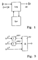
- Fig. 2 shows a preferred embodiment of an arrangement according to the invention for decoding a 7B / 8B-coded serial data stream 01, which consists of 8-bit groups of bits and has no bits characterizing the frame structure.
- the data stream ⁇ 1 is read into a series / parallel converter SPW with a read clock T 1 and output as a sequence of 8-bit parallel bit groups ⁇ 11 to ⁇ 18 in parallel with a clock speed of 1/8 T 1, the first bit of each Parallel bit groups ⁇ 11 to ⁇ 18 is the coding bit ⁇ 11 and the remaining bits form a parallel signal bit group ⁇ 12 to ⁇ 18.
- the parallel signal bit groups ⁇ 12 to ⁇ 18 are inverted in an inverter I with an associated coding bit ⁇ 11 carrying the logical value 1 or not inverted with a logical value 0.
- the parallel signal bit groups ⁇ 12 + to ⁇ 18 + arrive at an evaluator B, which determines the number of bits with the logical value 1 within each parallel signal bit group and forwards this value as a binary number to the first input of a comparator V.
- a subsequent AND gate U is activated, so that a coding bit 0 11, which is present at the AND gate U and indicates an inversion, can be switched through with the logical value 1 and as an error pulse to the input of a Frequency divider FT with the sub-ratio m: 1 arrives.
- the frequency divider FT emits a pulse to a clock suppression circuit TA, which suppresses a clock pulse from the input clock T 1 of the series / parallel converter SFW.
- This blanking shifts the 8-bit groups contained in the data stream ⁇ 1 by one bit each within the series / parallel converter SPW.
- the order of the signal bits and the coding bit is only cyclically interchanged, so that one of the signal bits controls the Invester.
- the frequency divider FT is set to zero at certain intervals by means of an erase clock T3 which is present at the reset input R.
- the clock frequency of this - preferably coming from a free-running oscillator - delete clock T3 must be greater than the product of the read clock T1 times the error probability divided by the division factor m of the frequency divider FT.
- FIG. 3 shows a further embodiment of the comparator V in FIG. 2.
- no comparison number is entered here and compared with the output signal of the evaluator B in an integrated module with a relatively high signal delay.
- a chip-carrier design of the decoder circuit according to FIG. 2 in ECL technology which has been practically implemented has been successfully tested for bit rates up to 560 Mbit / s.
Landscapes
- Engineering & Computer Science (AREA)
- Computer Networks & Wireless Communication (AREA)
- Signal Processing (AREA)
- Physics & Mathematics (AREA)
- Spectroscopy & Molecular Physics (AREA)
- Error Detection And Correction (AREA)
- Compression, Expansion, Code Conversion, And Decoders (AREA)
- Detection And Prevention Of Errors In Transmission (AREA)
- Reduction Or Emphasis Of Bandwidth Of Signals (AREA)
- Dc Digital Transmission (AREA)
Abstract
Description
Die Erfindung betrifft ein Verfahren und eine zugehörige Anordnung zur Decodierung eines nB/(n+1)B-codierten Datenstroms, der aus Wörtern oder Bitgruppen mit jeweils n Signalbits und einem eingefügten Codierbit besteht.The invention relates to a method and an associated arrangement for decoding an nB / (n + 1) B-coded data stream, which consists of words or groups of bits, each with n signal bits and an inserted coding bit.
Diese beispielsweise in dem Aufsatz von R. 0. Carter, nLow-Disparity Binary Coding System" in Electronics Letters, May 1965, Vol. 1, No. 3, Seiten 67 u. 68 beschriebene nB/(n+1)B-Codierung wird bekanntlich in der Nachrichtentechnik häufig dazu verwendet, um aus einem einfachen Binärcode einen Leitungscode zu erzeugen, dessen Frequenzspektrum keinen Gleichstromanteil und möglichst geringe Anteile bei tiefen Frequenzen hat, aber einen möglichst hohen Anteil bei der halben Bitfolgefrequenz hat, der möglichst noch unabhängig vom jeweiligen Informationsinhalt ist. Dabei folgt nach n nicht invertierten oder nach n invertierten Signalbits des ursprünglichen Binärcodes ein weiteres - (n+1) tes - Bit als Codierbit, das z. B. mit dem logischen Wert 1 bzw.,0 anzeigt, daß eine bzw. keine Invertierung der ursprünglichen n Signalbits sendeseitig oder auf der Übertragungsstrecke vorgenommen wurde, um in dem so gebildeten Datenstrom im zeitlichen Mittel eine möglichst gleiche Zahl von 0 - und 1-Bits zu erreichen.This nB / (n + 1) B- described for example in the article by R. 0. Carter, n Low-Disparity Binary Coding System "in Electronics Letters, May 1965, Vol. 1, No. 3, pages 67 and 68. As is well known, coding is often used in telecommunications to generate a line code from a simple binary code, the frequency spectrum of which has no DC component and as little as possible at low frequencies, but has as high a portion as possible at half the bit rate, which is as independent as possible of the respective one After n non-inverted or after n inverted signal bits of the original binary code, there follows another - (n + 1) test bit as coding bit, which, for example with the
Die Decodierung des nB(n+1)B-Codes auf der Empfangsseite erfolgt in bekannter Weise so, daß in dem ursprünglichen Code ein Rahmenaufbau vorausgesetzt wird, der in einer Synchronisierschaltung des Empfängers erkennbar ist und mit dessen Hilfe dann die exakte zeitliche Lager der n Signalbits und des Codierbits mittels einer Logik festgestellt wird. Je nach logischem Wert des Codierbits gibt dann die Logik die n zugehörigen Signalbits entweder invertiert oder aber unbeeinflußt als Ausgangssignal aus.The decoding of the nB (n + 1) B code on the receiving side is carried out in a known manner in such a way that a frame structure is required in the original code, which can be recognized in a synchronization circuit of the receiver and with the help of which the exact temporal storage of the n Signal bits and the coding bit is determined by means of logic. Depending on the logical value of the coding bit, the logic then outputs the n associated signal bits either inverted or uninfluenced as the output signal.
Fig. 1 zeigt dieses bekannte Prinzip einer üblichen Decodier-Schaltung. Ein empfangener nB/(n+1) B-codierter Datenstrom φ 1, - der aus einer fortlaufenden Aneinanderreihung von jeweils n Signalbits, einem Codierbit und weiteren Bits besteht, die den Rahmenaufbau kennzeichnen, - wird in einen Empfänger eingelesen, mit Hilfe der den Rahmenaufbau kennzeichnenden Bits in einer Synchronisierschaltung Syn synchronisiert und in einer Logikschaltung Log decodiert. Am Ausgang des Empfängers steht dann ein Datenstrom φ 2 zur Verfügung, der aus einer fortlaufenden Aneinanderreihung von jeweils n Signalbits und den den Rahmenaufbau kennzeichnenden Bits besteht.1 shows this known principle of a conventional decoding circuit. A received nB / (n + 1) B-coded
Dieses herkömmliche Verfahren der Decodierung hat den Nachteil, daß durch den Rahmenaufbau des ursprünglichen Codes die Anwendungsmöglichkeiten eingeschränkt sind und sich je nach Rahmenaufbau bzw. Rahmenlänge u.U. sehr lange Synchronisierzeiten ergeben können.This conventional method of decoding has the disadvantage that the possible uses are limited by the frame structure of the original code and may vary depending on the frame structure or frame length. can result in very long synchronization times.
Nachteilig ist weiterhin, daß durch die Einfügung der den Rahmenaufbau kennzeichnenden Bits die Übertragungsgeschwindigkeit der Nutzinformation sich verringert bzw. die Übertragungsgeschwindigkeit des Datenstroms 0 1 über die Übertragungsstrecke entsprechend erhöht werden muß. Dieser Nachteil tritt auch dann ein, wenn erst nach der Umcodierung des ursprünglichen Codes in den nB/(n+1)B-Code die Kennzeichnung des Rahmenaufbaues vorgenommen wird.A further disadvantage is that the transmission speed of the useful information is reduced by the insertion of the bits characterizing the frame structure or the transmission speed of the
Der Erfindung liegt somit die Aufgabe zugrunde, ein Verfahren anzugeben, das einen nB(n+1)B-Code auch bei Fehlen von den Rahmenaufbau kennzeichnenden Bits decodieren kann und weiterhin eine vergleichsweise sehr kurze Synchronisierzeit hat.The invention is therefore based on the object of specifying a method which can decode an nB (n + 1) B code even in the absence of bits characterizing the frame structure and furthermore has a comparatively very short synchronization time.
Diese Aufgabe wird durch die kennzeichnenden Merkmale des Anspruchs 1 gelöst. Eine zugehörige Anordnung und vorteilhafte Weiterbildungen der Erfindung sind in den Unteransprüchen gekennzeichnet.This object is achieved by the characterizing features of
Die mit der Erfindung erzielten Vorteile bestehen insbesondere darin, daß trotz Fehlens von dem Rahmenaufbau kennzeichnenden Bits eine sehr kurze Synchronisierzeit benötigt wird. Durch eine bevorzugte Weiterbildung mit paralleler Verarbeitung der Bits innerhalb des Empfängers können darüberhinaus sehr hohe Bitraten verarbeitet werden.The advantages achieved by the invention are, in particular, that a very short synchronization time is required in spite of the absence of bits which characterize the frame structure. A preferred further development with parallel processing of the bits within the receiver can also process very high bit rates.
Die Erfindung wird anhand eines in Fig. 2 und 3 dargestellten Ausführungsbeispiels im folgenden näher erläutert.The invention is explained in more detail below with reference to an embodiment shown in FIGS. 2 and 3.
Es zeigen
- Fig. 2 eine Schaltungsanordnung nach der Erfindung und
- Fig. 3 eine abgewandelte Ausführungsform eines Vergleichers der Schaltungsanordnung nach Fig. 2.
- Fig. 2 shows a circuit arrangement according to the invention and
- 3 shows a modified embodiment of a comparator of the circuit arrangement according to FIG. 2.
Dem in Fig. 2 dargestellten Ausführungsbeispiel ist als nB/(n+1)B-Code ein 7B/8B-Code zugrundegelegt. In diesem Code gehört zu jeweils 7 Bits des ursprünglichen Binärcodes ein Codierbit, so daß jeweils 8 Bits eine Bitgruppe bilden.The exemplary embodiment shown in FIG. 2 is based on a 7B / 8B code as the nB / (n + 1) B code. In this code, a coding bit belongs to every 7 bits of the original binary code, so that 8 bits each form a bit group.
Das Bildungsgesetz dieses ?B/8B-Code besteht bekanntlich darin, daß die n=7 Signalbits einer Bitgruppe dann und nur dann invertiert werden, wenn von den 7 Signalbits mehr als 4 Bits (![]()
![]()
Aus diesem Bildungsgesetz ergibt sich, daß bei fehlerfreiem Betrieb bei genau 4 Signalbits mit dem logischen Wert 1 innerhalb der 7 Signalbits das in der Bitgruppe als Codierbit stehende Bit niemals eine Invertierung der Signalbits anzeigen darf. Wenn trotzdem das Bit, das an der für das Codierbit festgelegten Stelle innerhalb der Bitgruppe steht, einen eine Invertierung der zugehörigen n=7 Signalsbits anzeigenden Wert hat (der im Ausführungsbeispiel der logische Wert 1 ist), so kann diese somit unzulässige Bitgruppe entweder durch einen Bitfehler verursacht worden sein oder es herrscht auf der Empfangsseite Asynchronität; hierbei tritt die unzulässige Bitgruppe mit sehr hoher Wahrscheinlichkeit auf.It follows from this law of formation that, when operating correctly with exactly 4 signal bits with the
Fig. 2 zeigt ein bevorzugtes Ausführungsbeispiel einer Anordnung nach der Erfindung zur Decodierung eines 7B/8B-codierten seriellen Datenstromes 01, der aus 8 Bit langen Bitgruppen besteht und keine den Rahmenaufbau kennzeichnenden Bits aufweist. Der Datenstrom φ 1 wird in einen Serien/Parallel-Wandler SPW mit einem Einlesetakt T 1 eingelesen und als eine Folge von 8-Bit-Parallelbitgruppen φ11 bis φ18 parallel mit einer Taktgeschwindigkeit von 1/8 T 1 ausgegeben, wobei jeweils das erste Bit dieser Parallelbitgruppen φ11 bis φ18 das Codierbit φ11 ist und die restlichen Bits eine Parallelsignaibitgruppe φ12 bis φ18 bilden.Fig. 2 shows a preferred embodiment of an arrangement according to the invention for decoding a 7B / 8B-coded
Gemäß der Codiervorschrift des nB/(n+1)B-Codes werden die Parallelsignalbitgruppen φ12 bis φ18 in einem Inverter I bei einem zugehörigen den logischen Wert 1 führenden Codierbit φ11 invertiert bzw. bei einem logischen Wert 0 nicht invertiert.According to the coding regulation of the nB / (n + 1) B code, the parallel signal bit groups φ12 to φ18 are inverted in an inverter I with an associated coding bit φ11 carrying the
Die den Inverter I verlassenden Parallelsignalbitgruppen φ12+ bis 0 18+ gelangen zu einem Parallel/Serien-Wandler PSW und werden dort als Ausgaugsbitstrom φ2 mit einem Takt T2 (=![]()
![]()
![]()
![]()
Gleichzeitig gelangen die Parallelsignalbitgruppen φ 12+ bis φ 18+ zu einem Bewerter B, der die Anzahl der Bits mit dem logischen Wert 1 innerhalb jeder Parallelsignal-Bitgruppe ermittelt und diesen Wert als Binärzahl an den ersten Eingang eines Vergleichers V weitergibt.At the same time, the parallel signal
An dessen zweiten Eingang ist die fest vorgegebene Zahl 4 = n+1 als Binärzahl aufgeschaltet. 2At its second input, the
Bei Übereinstimmung der Informationen an beiden Eingängen des Vergleichers V wird ein nachfolgendes UND-Glied U aktiviert, so daß ein gleichzeitig am UND-Glied U anstehendes eine Invertierung anzeigendes Codierbit 0 11 mit dem logischen Wert 1 durchgeschaltet werden kann und als Fehlerimpuls an den Eingang eines Frequenzteilers FT mit dem Teilverhältnis m : 1 gelangt.If the information at both inputs of the comparator V matches, a subsequent AND gate U is activated, so that a
Dieser Fall tritt nur jedesmal dann ein, wenn wie vorstehend erläutert eine unzulässige Bitgruppe vorliegt, und zwar durch Bitfehler sehr selten, durch Asynchronität aber sehr dicht gehäuft.This case only occurs whenever there is an impermissible bit group, as explained above, very rarely due to bit errors, but very densely due to asynchrony.
Nach m solcher unzulässigen Bitgruppen gibt der Frequenzteiler FT einenImpuls zu einer Taktausblendschaltung TA ab, welche einen Taktimpuls aus dem Eingangstakt T 1 des Serien/Parallel-Wandlers SFW ausblendet. Durch diese Ausblendung werden die in dem Datenstrom φ 1 enthaltenen 8-BitGruppen um jeweils ein Bit innerhalb des Serien/Parallel-Wandlers SPW verschoben. Bei Asynchronität ist in diesem nämlich die Reihenfolge der Signalbits und des Codierbits lediglich zyklisch vertauscht, so daß eines der Signalbits den Invester steuert.After m such inadmissible bit groups, the frequency divider FT emits a pulse to a clock suppression circuit TA, which suppresses a clock pulse from the
Treten unzulässige Bitgruppen durch Asynchronität auf, so ist spätestens nach n Taktimpulsausblendungen die Synchronität hergestellt, was einer Anzahl von maximal n x m unzulässiger Bitgruppen entspricht.If inadmissible bit groups occur due to asynchrony, the synchronicity is established at the latest after n clock pulse suppression, which corresponds to a maximum number of n x m inadmissible bit groups.
Um unnötige bzw. störende Auslösung von Synchronisierschritten bei lediglich durch Bitfehler mit normaler Fehlerrate verursachten unzulässigen Bitgruppen zu unterbinden, wird der Frequenzteiler FT mittels eines Löschtaktes T3, der am Rücksetzeingang R anliegt, in bestimmten Zeitabständen auf Null gesetzt. Die Taktfrequenz dieses -vorzugsweise aus einem freilaufenden Oszillators kommenden - Löschtaktes T3 muß größer sein als das Produkt aus dem Einlesetakt T1 mal der Fehlerwahrscheinlichkeit dividiert durch den Teilungsfaktor m des Frequenzteilers FT.In order to prevent unnecessary or disruptive triggering of synchronization steps in the case of inadmissible bit groups caused solely by bit errors with a normal error rate, the frequency divider FT is set to zero at certain intervals by means of an erase clock T3 which is present at the reset input R. The clock frequency of this - preferably coming from a free-running oscillator - delete clock T3 must be greater than the product of the read clock T1 times the error probability divided by the division factor m of the frequency divider FT.
Fig. 3 zeigt eine weitere Ausführungsform des Vergleichers V in Fig 2. Anders als beim Vergleicher V in Fig.2 wird hier keine Vergleichszahl eingegeben und in einem integrierten Baustein mit verhältnismäßig hoher Signal Verzögerung mit dem Ausgangssignal des Bewerters B verglichen. Vielmehr nimmt hier durch eine feste Verschaltung von zwei Negier-Gliedern VN1 und VN2 mit einem UND-Glied VU dessen Ausgang nur dann den logischen Wert 1 an, wenn am Eiagang vom Bewerter her die Zahl 4=(n+1) in digitaler Codierung (100) anliegt.3 shows a further embodiment of the comparator V in FIG. 2. In contrast to the comparator V in FIG. 2, no comparison number is entered here and compared with the output signal of the evaluator B in an integrated module with a relatively high signal delay. Rather, through a fixed interconnection of two negation gates VN1 and VN2 with an AND gate VU, its output assumes the
Ein Chip-carrier-Bauweise praktisch ausgeführter Aufbau der Decodierschaltung nach Fig. 2 in ECL-Technik wurde für Bitraten bis 560 Mbit/s erfolgreich erprobt.A chip-carrier design of the decoder circuit according to FIG. 2 in ECL technology which has been practically implemented has been successfully tested for bit rates up to 560 Mbit / s.
Claims (4)
Priority Applications (1)
| Application Number | Priority Date | Filing Date | Title |
|---|---|---|---|
| AT84105259T ATE38112T1 (en) | 1983-05-13 | 1984-05-09 | METHOD AND ARRANGEMENT FOR DECODING AN N.B/(N+1)B ENCODED DATA STREAM. |
Applications Claiming Priority (2)
| Application Number | Priority Date | Filing Date | Title |
|---|---|---|---|
| DE3317466 | 1983-05-13 | ||
| DE19833317466 DE3317466A1 (en) | 1983-05-13 | 1983-05-13 | METHOD AND DEVICE FOR DECODING AN NB / (N + 1) B-CODED DATA FLOW |
Publications (3)
| Publication Number | Publication Date |
|---|---|
| EP0126384A2 true EP0126384A2 (en) | 1984-11-28 |
| EP0126384A3 EP0126384A3 (en) | 1986-04-16 |
| EP0126384B1 EP0126384B1 (en) | 1988-10-19 |
Family
ID=6198912
Family Applications (1)
| Application Number | Title | Priority Date | Filing Date |
|---|---|---|---|
| EP84105259A Expired EP0126384B1 (en) | 1983-05-13 | 1984-05-09 | Method and arrangement for decoding an nb/(n+1)b-coded data stream |
Country Status (4)
| Country | Link |
|---|---|
| EP (1) | EP0126384B1 (en) |
| JP (1) | JPS60100832A (en) |
| AT (1) | ATE38112T1 (en) |
| DE (2) | DE3317466A1 (en) |
Cited By (3)
| Publication number | Priority date | Publication date | Assignee | Title |
|---|---|---|---|---|
| WO1991015926A1 (en) * | 1990-04-10 | 1991-10-17 | British Telecommunications Public Limited Company | Data alignment |
| WO1994016507A1 (en) * | 1993-01-14 | 1994-07-21 | Apple Computer, Inc. | Delay line separator for data bus |
| EP1170914A2 (en) * | 2000-07-07 | 2002-01-09 | Infineon Technologies AG | Method and apparatus for digitally coding binary data with a particular transmission spectrum |
Citations (2)
| Publication number | Priority date | Publication date | Assignee | Title |
|---|---|---|---|---|
| US3185963A (en) * | 1960-11-25 | 1965-05-25 | Stelma Inc | Synchronizing system having reversible counter means |
| US3241067A (en) * | 1961-04-21 | 1966-03-15 | Bell Telephone Labor Inc | Synchronization of decoder systems based on message wave statistics |
Family Cites Families (1)
| Publication number | Priority date | Publication date | Assignee | Title |
|---|---|---|---|---|
| JPS57162850A (en) * | 1981-03-31 | 1982-10-06 | Fujitsu Ltd | Code error detecting system |
-
1983
- 1983-05-13 DE DE19833317466 patent/DE3317466A1/en not_active Withdrawn
-
1984
- 1984-05-09 DE DE8484105259T patent/DE3474748D1/en not_active Expired
- 1984-05-09 AT AT84105259T patent/ATE38112T1/en not_active IP Right Cessation
- 1984-05-09 EP EP84105259A patent/EP0126384B1/en not_active Expired
- 1984-05-10 JP JP59091984A patent/JPS60100832A/en active Granted
Patent Citations (2)
| Publication number | Priority date | Publication date | Assignee | Title |
|---|---|---|---|---|
| US3185963A (en) * | 1960-11-25 | 1965-05-25 | Stelma Inc | Synchronizing system having reversible counter means |
| US3241067A (en) * | 1961-04-21 | 1966-03-15 | Bell Telephone Labor Inc | Synchronization of decoder systems based on message wave statistics |
Non-Patent Citations (1)
| Title |
|---|
| CONFERENCE RECORD OF THE IEEE INTERNATIONAL CONFERENCE ON COMMUNICATIONS (ICC83), Band 2 vom 3, 19.-22. Juni 1983, Seiten 690-694, Boston, Massachusetts; IEEE New York, US; G. HANKE: "Fast 7B/8B coder and decoder for an optical transmission system" * |
Cited By (6)
| Publication number | Priority date | Publication date | Assignee | Title |
|---|---|---|---|---|
| WO1991015926A1 (en) * | 1990-04-10 | 1991-10-17 | British Telecommunications Public Limited Company | Data alignment |
| WO1994016507A1 (en) * | 1993-01-14 | 1994-07-21 | Apple Computer, Inc. | Delay line separator for data bus |
| US5412697A (en) * | 1993-01-14 | 1995-05-02 | Apple Computer, Inc. | Delay line separator for data bus |
| US5619541A (en) * | 1993-01-14 | 1997-04-08 | Apple Computer, Inc. | Delay line separator for data bus |
| EP1170914A2 (en) * | 2000-07-07 | 2002-01-09 | Infineon Technologies AG | Method and apparatus for digitally coding binary data with a particular transmission spectrum |
| EP1170914A3 (en) * | 2000-07-07 | 2004-10-06 | Infineon Technologies AG | Method and apparatus for digitally coding binary data with a particular transmission spectrum |
Also Published As
| Publication number | Publication date |
|---|---|
| DE3474748D1 (en) | 1988-11-24 |
| EP0126384A3 (en) | 1986-04-16 |
| EP0126384B1 (en) | 1988-10-19 |
| ATE38112T1 (en) | 1988-11-15 |
| JPS6366085B2 (en) | 1988-12-19 |
| JPS60100832A (en) | 1985-06-04 |
| DE3317466A1 (en) | 1984-11-15 |
Similar Documents
| Publication | Publication Date | Title |
|---|---|---|
| DE19736434C2 (en) | Methods and devices for recognizing the position of data packets lying in a serial data reception stream | |
| DE69432587T2 (en) | DELAY LINE SEPARATOR FOR DATA BUS | |
| DE3779820T2 (en) | DIGITAL PHASE CONTROL LOOP. | |
| DE68923207T2 (en) | Circuit for preventing a metastable state. | |
| DE2121115C2 (en) | Test device for non-linear circuits | |
| DE2320422A1 (en) | PROCEDURE FOR ERROR DETECTION | |
| EP0325318B1 (en) | Switching exchange | |
| DE3442613C2 (en) | ||
| DE3786041T2 (en) | Communication bit pattern recognition circuit. | |
| DE3780406T2 (en) | METHOD AND ARRANGEMENT FOR CODING AND DECODING BINARY INFORMATION. | |
| DE2842371A1 (en) | METHOD FOR SYNCHRONIZING TRANSMITTER AND RECEIVER DEVICES | |
| EP0126384B1 (en) | Method and arrangement for decoding an nb/(n+1)b-coded data stream | |
| DE1934869B2 (en) | PROCEDURE AND CIRCUIT ARRANGEMENT FOR CODING ASYNCHRONOUS BINARY DIGITAL SIGNALS | |
| DE68919211T2 (en) | Serial data receiver. | |
| EP0725517B1 (en) | Method for initializing a network | |
| EP0591231B1 (en) | Process for determining the origin of bit errors | |
| DE69120364T2 (en) | Method and device for perceiving a frame bit sequence in a digital data transmission system | |
| EP0570813A2 (en) | Method and apparatus for reconstruction the correct sequence of ATM-celle | |
| DE2326658A1 (en) | DATA SEPARATION DEVICE | |
| DE19813965C1 (en) | Digital data pulse transmission method | |
| DE2647716B1 (en) | Path section monitor for PCM TDMA system - replaces first frame identification word with second word during alarm indication | |
| EP0403856B1 (en) | Method and circuit for auxiliary data flow transmission | |
| EP1126615A1 (en) | Clock frequency dividing method and frequency divider for realising said method | |
| DE4140920C1 (en) | Level changing circuitry for flanks of rectangular or trapezoidal signals - has threshold value discriminator with output signal separated into two channels, each having a gate circuit assigned to SR-flip=flop | |
| DE3801220A1 (en) | Multi-stage binary counter equipped for test runs |
Legal Events
| Date | Code | Title | Description |
|---|---|---|---|
| PUAI | Public reference made under article 153(3) epc to a published international application that has entered the european phase |
Free format text: ORIGINAL CODE: 0009012 |
|
| AK | Designated contracting states |
Designated state(s): AT BE CH DE FR GB IT LI NL SE |
|
| PUAL | Search report despatched |
Free format text: ORIGINAL CODE: 0009013 |
|
| AK | Designated contracting states |
Kind code of ref document: A3 Designated state(s): AT BE CH DE FR GB IT LI NL SE |
|
| 17P | Request for examination filed |
Effective date: 19860923 |
|
| 17Q | First examination report despatched |
Effective date: 19880322 |
|
| GRAA | (expected) grant |
Free format text: ORIGINAL CODE: 0009210 |
|
| AK | Designated contracting states |
Kind code of ref document: B1 Designated state(s): AT BE CH DE FR GB IT LI NL SE |
|
| PG25 | Lapsed in a contracting state [announced via postgrant information from national office to epo] |
Ref country code: SE Effective date: 19881019 |
|
| REF | Corresponds to: |
Ref document number: 38112 Country of ref document: AT Date of ref document: 19881115 Kind code of ref document: T |
|
| GBT | Gb: translation of ep patent filed (gb section 77(6)(a)/1977) | ||
| REF | Corresponds to: |
Ref document number: 3474748 Country of ref document: DE Date of ref document: 19881124 |
|
| ET | Fr: translation filed | ||
| ITF | It: translation for a ep patent filed | ||
| PG25 | Lapsed in a contracting state [announced via postgrant information from national office to epo] |
Ref country code: GB Effective date: 19890509 Ref country code: AT Effective date: 19890509 |
|
| PG25 | Lapsed in a contracting state [announced via postgrant information from national office to epo] |
Ref country code: BE Effective date: 19890531 |
|
| PGFP | Annual fee paid to national office [announced via postgrant information from national office to epo] |
Ref country code: DE Payment date: 19890726 Year of fee payment: 6 |
|
| PLBE | No opposition filed within time limit |
Free format text: ORIGINAL CODE: 0009261 |
|
| STAA | Information on the status of an ep patent application or granted ep patent |
Free format text: STATUS: NO OPPOSITION FILED WITHIN TIME LIMIT |
|
| PGFP | Annual fee paid to national office [announced via postgrant information from national office to epo] |
Ref country code: CH Payment date: 19890824 Year of fee payment: 6 |
|
| 26N | No opposition filed | ||
| PG25 | Lapsed in a contracting state [announced via postgrant information from national office to epo] |
Ref country code: NL Effective date: 19891201 |
|
| GBPC | Gb: european patent ceased through non-payment of renewal fee | ||
| NLV4 | Nl: lapsed or anulled due to non-payment of the annual fee | ||
| PG25 | Lapsed in a contracting state [announced via postgrant information from national office to epo] |
Ref country code: FR Free format text: LAPSE BECAUSE OF NON-PAYMENT OF DUE FEES Effective date: 19900131 |
|
| REG | Reference to a national code |
Ref country code: FR Ref legal event code: ST |
|
| PG25 | Lapsed in a contracting state [announced via postgrant information from national office to epo] |
Ref country code: LI Effective date: 19900531 Ref country code: CH Effective date: 19900531 |
|
| REG | Reference to a national code |
Ref country code: CH Ref legal event code: PL |
|
| PG25 | Lapsed in a contracting state [announced via postgrant information from national office to epo] |
Ref country code: DE Effective date: 19910201 |