EP0125044B1 - Microcomputer with interprocess communication - Google Patents
Microcomputer with interprocess communication Download PDFInfo
- Publication number
- EP0125044B1 EP0125044B1 EP84302480A EP84302480A EP0125044B1 EP 0125044 B1 EP0125044 B1 EP 0125044B1 EP 84302480 A EP84302480 A EP 84302480A EP 84302480 A EP84302480 A EP 84302480A EP 0125044 B1 EP0125044 B1 EP 0125044B1
- Authority
- EP
- European Patent Office
- Prior art keywords
- channel
- communication
- processes
- instruction
- input
- Prior art date
- Legal status (The legal status is an assumption and is not a legal conclusion. Google has not performed a legal analysis and makes no representation as to the accuracy of the status listed.)
- Expired
Links
Images


Classifications
-
- G—PHYSICS
- G06—COMPUTING; CALCULATING OR COUNTING
- G06F—ELECTRIC DIGITAL DATA PROCESSING
- G06F9/00—Arrangements for program control, e.g. control units
- G06F9/06—Arrangements for program control, e.g. control units using stored programs, i.e. using an internal store of processing equipment to receive or retain programs
- G06F9/46—Multiprogramming arrangements
- G06F9/48—Program initiating; Program switching, e.g. by interrupt
- G06F9/4806—Task transfer initiation or dispatching
- G06F9/4843—Task transfer initiation or dispatching by program, e.g. task dispatcher, supervisor, operating system
- G06F9/4881—Scheduling strategies for dispatcher, e.g. round robin, multi-level priority queues
-
- G—PHYSICS
- G06—COMPUTING; CALCULATING OR COUNTING
- G06F—ELECTRIC DIGITAL DATA PROCESSING
- G06F9/00—Arrangements for program control, e.g. control units
- G06F9/06—Arrangements for program control, e.g. control units using stored programs, i.e. using an internal store of processing equipment to receive or retain programs
- G06F9/46—Multiprogramming arrangements
- G06F9/52—Program synchronisation; Mutual exclusion, e.g. by means of semaphores
Definitions
- the invention relates to microcomputers with interprocess communication and is an improvement relating to the microcomputer described in our European Patent Application 0113516.
- the above mentioned applications describe an improved microcomputer comprising a single integrated circuit device having a processor and memory in the form of RAM on the same integrated circuit device, the processor being arranged to operate in accordance with functions selected from a function set.
- Said function set includes direct functions and indirect functions, the indirect functions being used to select one of a variety of "operations".
- Said operations include the operation "synchronise” which is used to permit two processes to communicate with each other, the two processes being either on the same microcomputer or in other cases the two processes may be on separate respective microcomputers.
- use of the operation "synchronise” has required two word locations in memory to provide a channel permitting process to process communication on the same microcomputer.
- process to process communication requires that each process includes in its program sequence two operations of "synchronise" for each message transmission in order to ensure than the message transmission occurs when the two processes are at corresponding stages in their program sequences. In some circumstances this may cause a process to be descheduled twice in order to effect synchronised message transmission.
- the present invention provides a method operating concurrent processes in a microcomputer system having at least one processor and memory wherein each of said concurrent processes executes a plurality of instructions included in respective programs, said instructions including communication instructions to output data and input data, the method comprising the steps of (1) decoding instructions from one of said programs to execute a current process, (2) scheduling a plurality of said processes for execution by a processor, including identifying one or more processes which form a collection awaiting execution by a processor, descheduling a process by interrupting execution of instructions by the process, and scheduling a process by adding it to said collection, and (3) effecting synchronised communication between a communicating pair of said processes which each include a communication instruction in its program, said communication including identifying a channel for use in synchronising communication between said pair of processes, storing in said channel a value indicating whether either of said pair of communicating processes has reached a communication instruction in its program requiring communication through said channel, and in response to execution of a communication instruction by one of said pair of communicating processes testing the value held in said channel, characterised by
- microcomputer relates to small sized computers generally based on integrated circuit devices but it does not impose any limit on how small the computer may be.
- the invention also provides a microcomputer for use in carrying out the aforesaid method, said microcomputer comprising memory and a processor operable to execute a plurality of concurrent processes having sequential instructions in respective programs, said instructions including communication instructions to output or input data, instruction decoding means for decoding instructions which are executed by a current process, process scheduling means having means for identifying one or more processes which form a collection awaiting execution by the processor, means for descheduling a process by interrupting execution of the current process, and means for scheduling a process by adding it to said collection, and synchronised communication means for effecting synchronised communication between a communicating pair of said processes, said synchronised communication means comprising a synchronising channel having store means for holding either a first value indicating that one of said pair of processes has reached a communication instruction in its program requiring communication through said channel, or another value indicating that neither process of said pair has reached a communication and instruction requiring communication through said channel, characterised by control means (10, 12, 13) responsive to execution of a communication instruction by one of said pair of
- the microcomputer comprises an integrated circuit device including a plurality of channels some in the form of registers and some provided by memory locations in memory on the same integrated circuit device as the processor.
- the channel provided by memory locations each comprise a single word location.
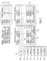
- the microcomputer described in this example comprises an integrated circuit device in the form of a single silicon chip having both a processor and memory in the form of RAM as well as links to permit external communication.
- the main elements of the microcomputer are illustrated in Figure 1 on a single silicon chip 11 using p-well complementary MOS technology.
- a control processing unit (CPU) 12 is provided with some read-only memory (ROM) 13 and is coupled to a memory interface 14 controlled by interface control logic 15.
- the CPU 12 incorporates an arithmetic logic unit (ALU), registers and data paths some of which are illustrated in Figure 2.
- the CPU 12 and memory interface 14 are connected to a bus 16 which provides interconnection between the elements on the chip 11.
- a service system 17 is provided with a plurality of input pins 18.
- the microcomputer is provided with a random access memory (RAM) 19 and ROM 20 and the amount of memory on the chip is not less than 1K byte so that the processor 12 can be operated without external memory.
- the memory on the chip is at least 4K bytes.
- An external memory interface 23 is provided and connected to a plurality of pins 24 for connection to an optional external memory.
- a plurality of serial links 25 are provided having input and output pins. The input and output pins of one serial link may each be connected by a single wire, non-shared unidirectional connection, to the corresponding output and input pins of a serial link on another microcomputer.
- Each serial link is connected to a synchronisation logic unit 10 comprising process scheduling logic.
- the CPU 12 includes a plurality of registers the following of which are shown in Figure 2:-
- the CPU also includes the arithmetic logic unit 37 and the contents of the CPU are interconnected to permit data transfer to and from said registers under the control of a microprogram held in a microinstruction ROM 13 (see Figure 4), which is arranged to respond to "input” and "output” operations defined below.
- Figure 2 also illustrates a workspace region 40 provided in the memory 19 for a process X as well as a workspace region 41 for a process Y.
- Each workspace comprises a plurality of addressable locations as indicated arranged to hold a plurality of variables associated with the process as well as the value IPTR to indicate the program stage for that process when it is next rescheduled together with a pointer to the WPTR of the next process in a collection of processes awaiting execution by the processor.
- Figure 2 also indicates four memory channels 50, 51, 52 and 53 each comprising a single word addressable location in the memory 19. It will be understood that the number of channels is not limited to four and any number of channels may be provided as required.
- FIG 2 also illustrates the provision of serial link registers which are each addressable in the same way as the memory channels or other memory locations.
- Each serial link 25 includes an input data register 60, an input process register 61, an output data register 62 and an output process register 63.
- Figure 4 illustrates a network comprising two interconnected microcomputers 11a and 11b and for simplicity only one serial link is shown in block form on each of these microcomputers.
- the output process registers of each link form an output channel having associated with it an output data register as well as output control logic 70 which includes an output control state machine 71 and an output data state machine 72.
- the input process register forms an input channel having associated with it an input data register as well as input control logic 73 including an input control state machine 74 and an input data state machine 75.
- the control logic 70 and 73 as well as the control and data state machines are constructed and operated as described in the above mentioned patent applications with the exception of the succession of states of the control state machines and this will be described below.
- the output data register 62 is connected to an output pin 80 which is connected by a single non-shared unidirectional wire 81 to an input pin 82 connected to the input data register 66.
- the output data register 64 is connected via an output pin 83 through a single non-shared unidirectional wire 84 to an input pin 85 connected to the input data register 60.
- the program sequence for each process includes a succession of instructions incorporating functions and operations as described in the abovementioned patent applications.
- the present example provides an improved microcomputer which has improved performance due to the use of fewer operations during process to process communication and furthermore less memory space is required to implement a communication channel as each of the above mentioned channels 50 to 53 involves a single word location only rather than the two word locations for the channels 40 to 43 of the above mentioned patent applications.
- These changes are effected in the present example by arranging for the microcomputer to respond to additional operations entitled "input” and "output” which may be added to the list of operations given in the above mentioned patent applications and these additional operations may have code number 16 and 17.
- the address of the channel to be used in the communication is loaded into AREGTR 35 so that the expression memory [AREG] identifies the channel.
- the contents of that channel are loaded into the OREGTR 31 so that the value in the channel is tested by the microcomputer to determine the state of the channel.
- line 3 indicates various alternatives that may follow depending on the result of testing the contents of the OREGTR.
- the contents of the OREGTR may indicate that the channel already holds a first special value NIL, or a second special value READY or a third special value representing the workspace pointer of a descheduled process which has already executed an instruction to effect data transmission using that channel.
- the channel to be used in the message communication will be a single memory location having a plurality of bit positions with a single address such as a single word location.
- a single address such as a single word location.
- such a channel can only contain either the first special value NIL or the WPTR of a descheduled process.
- process X If process X is to execute an output instruction, it first identifies the address of the channel 50 by loading the address of channel 50 into the AREGTR and the data to be transmitted is loaded into the BREGTR. On execution of the output instruction by process X, the contents of channel 50 are tested and in accordance with Figure 3 found to represent the first special value NIL.
- Figure 3 illustrates a sequence of stages each carrying the subscript a, b and c and the condition NIL is represented at 50a.
- process X causes the data to be transferred from the BREGTR into location 90 of its own workspace (as indicated at 90b) and its workspace pointer is loaded into the channel as indicated at 50b.
- Process X then executes a "wait" procedure which deschedules process X.
- Process X now waits until process Y is ready to input the data.
- process Y approaches the corresponding stage of its program, it identifies the channel 50 by loading the address of channel 50 into the AREGTR and carries out an input instruction which on executing lines 2 and 3 of the input definition, locates the workspace pointer of process X in channel 50.
- process Y then carries out lines 14 to 16 of the input definition.
- This causes the data stored in the workspace location 90 of process X to be copied into location 91 of the workspace of process Y as indicated at 91 c. It also loads the first special value NIL into channel 50 as indicated at 50c. It then causes a "run" procedure for process X which adds process X to the end of the list awaiting process operation. This is the position shown at the end of the sequence in Figure 3 with process Y having continued without interruption and process X waiting on a list.
- the first of these is the condition in line 2 in which the contents of the OREGTR are not READY in which case the sequence of lines 4 and 5 is followed or alternatively the OREGTR does have the value READY as indicated in line 6 in which case no action is taken. This occurs in external communications which are to be described below.
- the effect of line 4 of the definition of run is to add the process which is to be scheduled to the end of the list by having its workspace pointer stored in the workspace of the process currently indicated as the last on the list and this is done at an offset of two from the WPTR of the process as indicated at address 10998 in Figure 2.
- the WPTR of the process being scheduled is entered into the LPTR REG 34 indicating that it is now the last on the list.
- the second special value "READY" is only applicable in communication between processes on different microcomputers and wiJI be described below.
- lines 6, 7 and 8 of that definition cause the data to be transferred from the BREGTR into the output data register 62, as this has an address which is an offset of one from the process register 63, and stores the workspace pointer of process X in the channel 63b and executes a "wait" procedure which deschedules process X. This is the position shown at 63b and 62b in Figure 5.
- the output control logic 70 due to changes in state of the state machines causes output of the data long line 81 to the input data register 66 of microcomputer 11 b. For the purposes of Figure 5, it will be assumed that process Y has already executed an input instruction prior to receipt of data in the data register 66.
- the process register 67 will have held the special value NIL as this was the reset condition caused by operation of the control state machine.
- Process Y will have tested the value in the channel and on finding NIL will have carried out lines 9 and 10 of the input definition.
- the workspace pointer of process Y will have been loaded into the process register 67 and process Y will have been descheduled by the wait procedure. This is the position shown at 67b and 66b in Figure 5 and is assumed to be the position when data is received via line 81 into the input data register 66.
- the input control logic 73 on microcomputer 11b then changes state on receipt of the data to generate an input request to the CPU 12 on line 94 of microcomputer 11b.
- the input control logic 73 on microcomputer 11 a then provides an output to the output control logic 70 causing an output request to the CPU 12 on the microcomputer 11a.
- the processor of microcomputer 11a looks for any input or output requests from the link logic as previously described and will find an output request from the logic associated with the output register 63 and will therefore follow the sequence defined in lines 11 to 13 of the definition of the procedure "wait". This causes the workspace pointer of process X to be loaded into the OREGTR, the special value READY is loaded into the process register 63 and process X is rescheduled.
- the input control logic of microcomputer 11 b would, following the above table for the input control state machine, change the value of the input process register 67 to special value READY so that subsequent execution of the input instruction by process Y would locate the special value READY and process Y would carry out the sequence according to lines 6 and 7 of the definition of input. This would mean that data would be transferred from the input data register 66 to the workspace of process Y and the special value NIL would be loaded into the process register 67 and process Y would continue without interruption.
- the microcomputer is arranged to effect communication between processes when both processes are at corresponding stages in their program sequences. If either process attempts to transmit data when the other is not at a corresponding stage, the process which initiates the transmission is held up until both processes are at corresponding stages.
- Each process involved in the communication requires only one input or output instruction in its program sequence so that neither process is descheduled more than once in order to effect the data transmission.
- the memory space occupied by communication channels is reduced in requiring only one word of memory for each channel.
- the input and output instructions allow for addressing of workspace locations. This is advantageous in reducing the number of instructions or operations required to permit process to process communication and it permits more efficient transfer of data into process workspace locations.
Description
- The invention relates to microcomputers with interprocess communication and is an improvement relating to the microcomputer described in our European Patent Application 0113516.
- The above mentioned applications describe an improved microcomputer comprising a single integrated circuit device having a processor and memory in the form of RAM on the same integrated circuit device, the processor being arranged to operate in accordance with functions selected from a function set. Said function set includes direct functions and indirect functions, the indirect functions being used to select one of a variety of "operations". Said operations include the operation "synchronise" which is used to permit two processes to communicate with each other, the two processes being either on the same microcomputer or in other cases the two processes may be on separate respective microcomputers. As can be seen from the above mentioned patent applications, use of the operation "synchronise" has required two word locations in memory to provide a channel permitting process to process communication on the same microcomputer. One word of the channel was used to indicate the state of the channel and the other word was used to hold data for communication through the channel. Furthermore, process to process communication requires that each process includes in its program sequence two operations of "synchronise" for each message transmission in order to ensure than the message transmission occurs when the two processes are at corresponding stages in their program sequences. In some circumstances this may cause a process to be descheduled twice in order to effect synchronised message transmission.
- It is an object of the present invention to provide an improved microcomputer wherein data transmission between processes may be effected by use of instructions which may result in improved performance due to the use of fewer instructions during process to process communication. It is a further object to implement a communication channel using less memory space.
- In a preferred embodiment, the "synchronise" operation referred to in the above mentioned patent applications can be replaced by "input"' and "output" operations as described below.
- The present invention provides a method operating concurrent processes in a microcomputer system having at least one processor and memory wherein each of said concurrent processes executes a plurality of instructions included in respective programs, said instructions including communication instructions to output data and input data, the method comprising the steps of (1) decoding instructions from one of said programs to execute a current process, (2) scheduling a plurality of said processes for execution by a processor, including identifying one or more processes which form a collection awaiting execution by a processor, descheduling a process by interrupting execution of instructions by the process, and scheduling a process by adding it to said collection, and (3) effecting synchronised communication between a communicating pair of said processes which each include a communication instruction in its program, said communication including identifying a channel for use in synchronising communication between said pair of processes, storing in said channel a value indicating whether either of said pair of communicating processes has reached a communication instruction in its program requiring communication through said channel, and in response to execution of a communication instruction by one of said pair of communicating processes testing the value held in said channel, characterised by continuing the execution of instructions of the current process if the channel contains a value indicating that the other of the pair of communicating processes has already reached a communication instruction requiring communication through said channel, or descheduling said one of the communicating processes if the channel does not contain a value indicating that the other of the pair of communicating processes has already reached a communication instruction requiring communication through said channel, whereby both processes in said pair are at corresponding program instructions when said communication is effected and the pair of communicating processes each have a single communication instruction in its program sequence to effect said communication so that neither process of said pair is descheduled more than once to effect said synchronised communication.
- It will be understood that the term microcomputer relates to small sized computers generally based on integrated circuit devices but it does not impose any limit on how small the computer may be.
- The invention also provides a microcomputer for use in carrying out the aforesaid method, said microcomputer comprising memory and a processor operable to execute a plurality of concurrent processes having sequential instructions in respective programs, said instructions including communication instructions to output or input data, instruction decoding means for decoding instructions which are executed by a current process, process scheduling means having means for identifying one or more processes which form a collection awaiting execution by the processor, means for descheduling a process by interrupting execution of the current process, and means for scheduling a process by adding it to said collection, and synchronised communication means for effecting synchronised communication between a communicating pair of said processes, said synchronised communication means comprising a synchronising channel having store means for holding either a first value indicating that one of said pair of processes has reached a communication instruction in its program requiring communication through said channel, or another value indicating that neither process of said pair has reached a communication and instruction requiring communication through said channel, characterised by control means (10, 12, 13) responsive to execution of a communication instruction by one of said pair of processes to test the contents of said channel (50, 60, 61) said control means being operable in response to location of said first value in said channel (50,60,61) to continue executing instructions of the current process and operable in response to location of a said another value in said channel (50, 60, 61) to deschedule the current process whereby both processes in said pair are at corresponding program instructions when said communication is effected and neither process of said pair is descheduled more than once to effect said synchronised communication.
- In a preferred embodiment, the microcomputer comprises an integrated circuit device including a plurality of channels some in the form of registers and some provided by memory locations in memory on the same integrated circuit device as the processor. Preferably the channel provided by memory locations each comprise a single word location.
- An embodiment of the invention will now be described by way of example and with reference to the accompanying drawings in which:-
- Figure 1 is a block diagram showing the main features of the microcomputer,
- Figure 2 shows an arrangement of memory workspaces, registers, memory channels and serial links in the microcomputer,
- Figure 3 illustrates a succession of states of two workspace locations and one memory channel during process to process communication on one microcomputer,
- Figure 4 illustrates a network of two interconnected microcomputers permitting process to process communication from one microcomputer to the other, and
- Figure 5 shows a sequence of states for process and data registers in the microcomputers shown in Figure 4 during process to process communication between the two microcomputers.
- The microcomputer described in this example comprises an integrated circuit device in the form of a single silicon chip having both a processor and memory in the form of RAM as well as links to permit external communication. The main elements of the microcomputer are illustrated in Figure 1 on a
single silicon chip 11 using p-well complementary MOS technology. A control processing unit (CPU) 12 is provided with some read-only memory (ROM) 13 and is coupled to amemory interface 14 controlled byinterface control logic 15. TheCPU 12 incorporates an arithmetic logic unit (ALU), registers and data paths some of which are illustrated in Figure 2. TheCPU 12 andmemory interface 14 are connected to abus 16 which provides interconnection between the elements on thechip 11. Aservice system 17 is provided with a plurality ofinput pins 18. The microcomputer is provided with a random access memory (RAM) 19 andROM 20 and the amount of memory on the chip is not less than 1K byte so that theprocessor 12 can be operated without external memory. Preferably the memory on the chip is at least 4K bytes. Anexternal memory interface 23 is provided and connected to a plurality ofpins 24 for connection to an optional external memory. To allow the microcomputer to be linked to other microcomputers to form a network, a plurality ofserial links 25 are provided having input and output pins. The input and output pins of one serial link may each be connected by a single wire, non-shared unidirectional connection, to the corresponding output and input pins of a serial link on another microcomputer. Each serial link is connected to asynchronisation logic unit 10 comprising process scheduling logic. - The block diagram shown in Figure 1 corresponds to that included in the above mentioned European Patent Application No. 0113516. To avoid unnecessary repetition of description, the full details of the construction and operation of that microcomputer will not be set out below but the description in the above mentioned patent applications is hereby incorporated herein by reference.
- As described in the above mentioned patent applications, the
CPU 12 includes a plurality of registers the following of which are shown in Figure 2:-
- The CPU also includes the
arithmetic logic unit 37 and the contents of the CPU are interconnected to permit data transfer to and from said registers under the control of a microprogram held in a microinstruction ROM 13 (see Figure 4), which is arranged to respond to "input" and "output" operations defined below. - Figure 2 also illustrates a workspace region 40 provided in the
memory 19 for a process X as well as aworkspace region 41 for a process Y. Each workspace comprises a plurality of addressable locations as indicated arranged to hold a plurality of variables associated with the process as well as the value IPTR to indicate the program stage for that process when it is next rescheduled together with a pointer to the WPTR of the next process in a collection of processes awaiting execution by the processor. Figure 2 also indicates fourmemory channels memory 19. It will be understood that the number of channels is not limited to four and any number of channels may be provided as required. Figure 2 also illustrates the provision of serial link registers which are each addressable in the same way as the memory channels or other memory locations. Eachserial link 25 includes aninput data register 60, aninput process register 61, anoutput data register 62 and anoutput process register 63. Figure 4 illustrates a network comprising two interconnectedmicrocomputers 11a and 11b and for simplicity only one serial link is shown in block form on each of these microcomputers. The output process registers of each link form an output channel having associated with it an output data register as well asoutput control logic 70 which includes an outputcontrol state machine 71 and an outputdata state machine 72. The input process register forms an input channel having associated with it an input data register as well asinput control logic 73 including an inputcontrol state machine 74 and an inputdata state machine 75. Thecontrol logic - As can be seen from Figure 4, the
output data register 62 is connected to anoutput pin 80 which is connected by a single non-sharedunidirectional wire 81 to aninput pin 82 connected to theinput data register 66. Similarly theoutput data register 64 is connected via anoutput pin 83 through a single non-sharedunidirectional wire 84 to aninput pin 85 connected to theinput data register 60. - The program sequence for each process includes a succession of instructions incorporating functions and operations as described in the abovementioned patent applications.
- In order to effect message transmission between processes either on the same microcomputer or between processes on different microcomputers, the above mentioned patent applications use the operation called "synchronise" which has
code number 11 in the list of operations. - The present example provides an improved microcomputer which has improved performance due to the use of fewer operations during process to process communication and furthermore less memory space is required to implement a communication channel as each of the above mentioned
channels 50 to 53 involves a single word location only rather than the two word locations for the channels 40 to 43 of the above mentioned patent applications. These changes are effected in the present example by arranging for the microcomputer to respond to additional operations entitled "input" and "output" which may be added to the list of operations given in the above mentioned patent applications and these additional operations may havecode number -

- The procedure "run (OREG)" is defined as follows:

- As mentioned above, the succession of states of the output
control state machine 71 and the inputcontrol state machine 74 need modification from those described in the above mentioned patent applications in accordance with the following tables of successive states:- -

control state machine 74
- The way in which processes operate with input or output instructions will now be further described. The instructions are equally applicable to process to process communication on the same microcomputer or different microcomputers. In either case the process identifies a channel for use in the message transmission and that channel has an address either of a memory channel (such as 50 to 53) or a serial link provided by a process register (such as 61 or 63). In the above definitions of input and output as well as the procedures wait and run, line numbers have been added to each stage of the definition for ease of reference although the line numbers form no part of the definition. In both input and output instructions the first line indicates that a sequence of events is to occur the first of which is defined in
line number 2. The address of the channel to be used in the communication is loaded into AREGTR 35 so that the expression memory [AREG] identifies the channel. The contents of that channel are loaded into theOREGTR 31 so that the value in the channel is tested by the microcomputer to determine the state of the channel. In both the input and output instructions line 3 indicates various alternatives that may follow depending on the result of testing the contents of the OREGTR. The contents of the OREGTR may indicate that the channel already holds a first special value NIL, or a second special value READY or a third special value representing the workspace pointer of a descheduled process which has already executed an instruction to effect data transmission using that channel. In the case of an output instruction, if a test of the channel finds the special value NIL, the processor then carries out the sequence indicated inlines line 14 so that the processor then executes the sequence of three lines set out as 16, 17 and 18 of the output definition. Similarly, on execution of an input instruction, if testing of the OREGTR indicates that the channel has the special value READY, the processor follows the sequence of lines 6 and 7 of the input definition. If the channel has the special value NIL then the processor executes the sequence oflines lines 14 to 16 of the input definition. - In this case, the channel to be used in the message communication will be a single memory location having a plurality of bit positions with a single address such as a single word location. As will be explained below, such a channel can only contain either the first special value NIL or the WPTR of a descheduled process. This will now be described for message transmission between a process X wishing to communicate via
channel 50 with a process Y on the same microcomputer. Using the same memory location addresses as Figure 2, process X has aworkspace location 90 for a variable and process Y has aworkspace location 91 for a variable. Thechannel 50 has the same address as indicated in Figure 2. Thechannel 50 is a single word in memory providing a unidirectional communication channel which is shared by two and only two processes at any one time. If process X is to execute an output instruction, it first identifies the address of thechannel 50 by loading the address ofchannel 50 into the AREGTR and the data to be transmitted is loaded into the BREGTR. On execution of the output instruction by process X, the contents ofchannel 50 are tested and in accordance with Figure 3 found to represent the first special value NIL. Figure 3 illustrates a sequence of stages each carrying the subscript a, b and c and the condition NIL is represented at 50a. As the channel does not have the workspace pointer of process Y waiting to receive the data,lines 11 to 13 of the output definition are followed so that process X causes the data to be transferred from the BREGTR intolocation 90 of its own workspace (as indicated at 90b) and its workspace pointer is loaded into the channel as indicated at 50b. Process X then executes a "wait" procedure which deschedules process X. Process X now waits until process Y is ready to input the data. When process Y approaches the corresponding stage of its program, it identifies thechannel 50 by loading the address ofchannel 50 into the AREGTR and carries out an input instruction which on executinglines 2 and 3 of the input definition, locates the workspace pointer of process X inchannel 50. This meets the condition TRUE inline 12 of the input definition so that process Y then carries outlines 14 to 16 of the input definition. This causes the data stored in theworkspace location 90 of process X to be copied intolocation 91 of the workspace of process Y as indicated at 91 c. It also loads the first special value NIL intochannel 50 as indicated at 50c. It then causes a "run" procedure for process X which adds process X to the end of the list awaiting process operation. This is the position shown at the end of the sequence in Figure 3 with process Y having continued without interruption and process X waiting on a list. - As can be seen from the definition of the procedure "wait"
line 2 of the definition has the effect of storing an indication of the present program stage of the process at a workspace location having an offset of one from the workspace pointer for the process, as shown at 92 in Figure 2. Lines 3 to 13 of the definition of "wait" refer to external communications.Line 14 of the definition of "wait" causes theWPTR REG 32 to be loaded with a pointer to the next process on the list awaiting execution (taken fromlocation 93, which has an offset of 2 from the WPTR location as shown in Figure 2) andline 15 loads theregister 33 with the program stage indication of that process as soon as it becomes the current process. As can be seen from the definition of "run"line 2 sets out the possibility of two alternative situations. The first of these is the condition inline 2 in which the contents of the OREGTR are not READY in which case the sequence of lines 4 and 5 is followed or alternatively the OREGTR does have the value READY as indicated in line 6 in which case no action is taken. This occurs in external communications which are to be described below. The effect of line 4 of the definition of run is to add the process which is to be scheduled to the end of the list by having its workspace pointer stored in the workspace of the process currently indicated as the last on the list and this is done at an offset of two from the WPTR of the process as indicated ataddress 10998 in Figure 2. - According to line 5 of the definition of run, the WPTR, of the process being scheduled is entered into the
LPTR REG 34 indicating that it is now the last on the list. - The second special value "READY" is only applicable in communication between processes on different microcomputers and wiJI be described below.
- This will be described with reference to the sequence illustrated in Figure 5 representing an outputting process X on microcomputer 11 a transmitting a message via
line 81 to an inputting process Y onmicrocomputer 11b. Successive stages of the registers are marked with subscripts a to d in Figure 5. External communication is effected in generally similar manner using identical input and output operations although the control logical for the serial links may set the process registers to a second special value READY and they may also provide input or output requests onlines CPU 12 of each microcomputer in order to schedule any descheduled process. As can be seen from the tables showing the outputs from the control state machines, each output process register is reset to READY whereas each input process register is normally reset to NIL. This is the condition shown for theregister 63a and register 67a in Figure 5. For the process X to output data, it first loads the address of the channel, which in this case is theoutput process register 63, into the AREGTR and loads the data to be output into the BREGTR. On executing an output instruction the contents of the channel are loaded into the OREGTR and tested and as indicated at 63a in Figure 5, this detects the second special value READY due to the reset condition caused by the outputcontrol state machine 71. Thedata register 62a is marked EMPTY indicating that the relevant data has not yet been loaded into the register. It will be understood that the word EMPTY marked on a data register means that the contents of the register have no significance. In accordance with the definition of the output instruction, lines 6, 7 and 8 of that definition cause the data to be transferred from the BREGTR into the output data register 62, as this has an address which is an offset of one from theprocess register 63, and stores the workspace pointer of process X in thechannel 63b and executes a "wait" procedure which deschedules process X. This is the position shown at 63b and 62b in Figure 5. Theoutput control logic 70 due to changes in state of the state machines causes output of the datalong line 81 to the input data register 66 ofmicrocomputer 11 b. For the purposes of Figure 5, it will be assumed that process Y has already executed an input instruction prior to receipt of data in the data register 66. At the time the process Y executed the input instruction, the process register 67 will have held the special value NIL as this was the reset condition caused by operation of the control state machine. Process Y will have tested the value in the channel and on finding NIL will have carried outlines 9 and 10 of the input definition. In other words, the workspace pointer of process Y will have been loaded into theprocess register 67 and process Y will have been descheduled by the wait procedure. This is the position shown at 67b and 66b in Figure 5 and is assumed to be the position when data is received vialine 81 into the input data register 66. Theinput control logic 73 onmicrocomputer 11b then changes state on receipt of the data to generate an input request to theCPU 12 online 94 ofmicrocomputer 11b. In order to understand the effect of this, it is necessary to consider lines 3 to 7 of the definition of the procedure "wait". Whenever a process being executed bymicrocomputer 11 b is descheduled by a wait procedure, the CPU ofmicrocomputer 11 b looks for any external input request from a serial link as required by line 3 of the definition of procedure "wait". If there are no input requests it moves to line 9 of the definition where it looks for any external output request. In the definition of "wait" link [process] indicates the contents of a process register of serial link and link [data] indicates the contents of a data register of a serial link. The CPU services any input requests or output requests onlines CPU 12 ofmicrocomputer 11 next ceases executing a process, it will find an input request fromchannel 67 and this will cause the CPU to carry out lines 5 to 8 of the definition of the procedure "wait". This has the effect, due to lines 5 and 8, of rescheduling process Y, line 6 loads the value NIL into the process register as shown at 67b and line 7 causes the data from the input data register 66 to be transferred to the workspace of process Y. In addition, theinput control logic 73 provides an output signal to the output control logic which causes theoutput channel 65 to transmit an acknowledge signal vialine 84 to the microcomputer 11 a. Theinput control logic 73 on microcomputer 11 a then provides an output to theoutput control logic 70 causing an output request to theCPU 12 on the microcomputer 11a. When the processor of microcomputer 11a next deschedules a current process, the processor looks for any input or output requests from the link logic as previously described and will find an output request from the logic associated with theoutput register 63 and will therefore follow the sequence defined inlines 11 to 13 of the definition of the procedure "wait". This causes the workspace pointer of process X to be loaded into the OREGTR, the special value READY is loaded into theprocess register 63 and process X is rescheduled. It will be seen that in this sequence the output process and data registers 63 and 62 go through the changes indicated by the subscripts a, b and c in Figure 5 whereas the input process and data registers undergo the sequence illustrated by the subscripts a to d illustrated in Figure 5. - If in the above example data had been transferred via
line 81 to the input data register 66 of themicrocomputer 11 before process Y carried out an input instruction, the input control logic ofmicrocomputer 11 b would, following the above table for the input control state machine, change the value of the input process register 67 to special value READY so that subsequent execution of the input instruction by process Y would locate the special value READY and process Y would carry out the sequence according to lines 6 and 7 of the definition of input. This would mean that data would be transferred from the input data register 66 to the workspace of process Y and the special value NIL would be loaded into theprocess register 67 and process Y would continue without interruption. - It will be appreciated that in the above examples, the microcomputer is arranged to effect communication between processes when both processes are at corresponding stages in their program sequences. If either process attempts to transmit data when the other is not at a corresponding stage, the process which initiates the transmission is held up until both processes are at corresponding stages. Each process involved in the communication requires only one input or output instruction in its program sequence so that neither process is descheduled more than once in order to effect the data transmission. Furthermore, for communications between processes on the same microcomputer, the memory space occupied by communication channels is reduced in requiring only one word of memory for each channel. The input and output instructions allow for addressing of workspace locations. This is advantageous in reducing the number of instructions or operations required to permit process to process communication and it permits more efficient transfer of data into process workspace locations.
Claims (27)
Applications Claiming Priority (2)
| Application Number | Priority Date | Filing Date | Title |
|---|---|---|---|
| GB8309770 | 1983-04-11 | ||
| GB838309770A GB8309770D0 (en) | 1983-04-11 | 1983-04-11 | Microcomputer |
Publications (2)
| Publication Number | Publication Date |
|---|---|
| EP0125044A1 EP0125044A1 (en) | 1984-11-14 |
| EP0125044B1 true EP0125044B1 (en) | 1988-01-13 |
Family
ID=10540902
Family Applications (1)
| Application Number | Title | Priority Date | Filing Date |
|---|---|---|---|
| EP84302480A Expired EP0125044B1 (en) | 1983-04-11 | 1984-04-11 | Microcomputer with interprocess communication |
Country Status (6)
| Country | Link |
|---|---|
| US (1) | US4692861A (en) |
| EP (1) | EP0125044B1 (en) |
| JP (1) | JP2669816B2 (en) |
| DE (1) | DE3468759D1 (en) |
| GB (1) | GB8309770D0 (en) |
| WO (1) | WO1984004188A1 (en) |
Families Citing this family (19)
| Publication number | Priority date | Publication date | Assignee | Title |
|---|---|---|---|---|
| GB8329509D0 (en) * | 1983-11-04 | 1983-12-07 | Inmos Ltd | Computer |
| CA1244555A (en) * | 1985-06-17 | 1988-11-08 | Walter H. Schwane | Process transparent multi storage mode data transfer and buffer control |
| US4649473A (en) * | 1985-06-17 | 1987-03-10 | International Business Machines Corporation | Flexible data transmission for message based protocols |
| CA1244142A (en) * | 1985-06-17 | 1988-11-01 | William E. Hammer | Distributed data management mechanism |
| US4831518A (en) * | 1986-08-26 | 1989-05-16 | Bull Hn Information Systems Inc. | Multiprocessor interrupt rerouting mechanism |
| JPH0640324B2 (en) * | 1989-10-26 | 1994-05-25 | インターナショナル・ビジネス・マシーンズ・コーポレーション | Multiprocessor system and process synchronization method thereof |
| US5212790A (en) * | 1990-11-28 | 1993-05-18 | Teknekron Communications Systems, Inc. | Method of programming a task, having a plurality of processes, created by a plurality of different programmers, for operation by a computer |
| US5625845A (en) * | 1992-10-13 | 1997-04-29 | International Business Machines Corporation | System for facilitating continuous, real-time, unidirectional, and asynchronous intertask and end-device communication in a multimedia data processing system using open architecture data communication modules |
| JP2516317B2 (en) * | 1992-10-13 | 1996-07-24 | インターナショナル・ビジネス・マシーンズ・コーポレイション | Data processing system and method for loading digital signal processor. |
| GB2273591A (en) * | 1992-12-18 | 1994-06-22 | Network Systems Corp | Microcomputer control systems for interprogram communication and scheduling methods |
| US6539435B2 (en) * | 1995-06-21 | 2003-03-25 | International Business Machines Corporation | System and method for establishing direct communication between parallel programs |
| US5859981A (en) * | 1995-07-12 | 1999-01-12 | Super P.C., L.L.C. | Method for deadlock-free message passing in MIMD systems using routers and buffers |
| US6567839B1 (en) | 1997-10-23 | 2003-05-20 | International Business Machines Corporation | Thread switch control in a multithreaded processor system |
| US6212544B1 (en) | 1997-10-23 | 2001-04-03 | International Business Machines Corporation | Altering thread priorities in a multithreaded processor |
| US6697935B1 (en) | 1997-10-23 | 2004-02-24 | International Business Machines Corporation | Method and apparatus for selecting thread switch events in a multithreaded processor |
| US6076157A (en) * | 1997-10-23 | 2000-06-13 | International Business Machines Corporation | Method and apparatus to force a thread switch in a multithreaded processor |
| US6105051A (en) * | 1997-10-23 | 2000-08-15 | International Business Machines Corporation | Apparatus and method to guarantee forward progress in execution of threads in a multithreaded processor |
| US7454758B2 (en) * | 2004-02-05 | 2008-11-18 | Aol Llc, A Delaware Limited Liability Company | Inter-process communication on a computer |
| US8032354B2 (en) * | 2007-12-27 | 2011-10-04 | Nvidia Corporation | Method and system for communicating between two independent software components of a device |
Family Cites Families (10)
| Publication number | Priority date | Publication date | Assignee | Title |
|---|---|---|---|---|
| US3805247A (en) * | 1972-05-16 | 1974-04-16 | Burroughs Corp | Description driven microprogrammable multiprocessor system |
| FR2253428A5 (en) * | 1973-11-30 | 1975-06-27 | Honeywell Bull Soc Ind | |
| US4056846A (en) * | 1976-06-30 | 1977-11-01 | Ibm Corporation | Data processing system with apparatus for sharing channel background processing |
| US4177513A (en) * | 1977-07-08 | 1979-12-04 | International Business Machines Corporation | Task handling apparatus for a computer system |
| US4155117A (en) * | 1977-07-28 | 1979-05-15 | International Business Machines Corporation | Synchronizing channel-to-channel adapter |
| US4433376A (en) * | 1978-10-31 | 1984-02-21 | Honeywell Information Systems Inc. | Intersystem translation logic system |
| US4384324A (en) * | 1980-05-06 | 1983-05-17 | Burroughs Corporation | Microprogrammed digital data processing system employing tasking at a microinstruction level |
| JPS57768A (en) * | 1980-06-04 | 1982-01-05 | Hitachi Ltd | Message transmission and reception system between processor |
| US4466058A (en) * | 1981-10-02 | 1984-08-14 | Ncr Corporation | Method and apparatus for establishing priority between processing units having a common communication channel |
| US4449182A (en) * | 1981-10-05 | 1984-05-15 | Digital Equipment Corporation | Interface between a pair of processors, such as host and peripheral-controlling processors in data processing systems |
-
1983
- 1983-04-11 GB GB838309770A patent/GB8309770D0/en active Pending
-
1984
- 1984-04-11 JP JP59501680A patent/JP2669816B2/en not_active Expired - Lifetime
- 1984-04-11 WO PCT/GB1984/000124 patent/WO1984004188A1/en unknown
- 1984-04-11 US US06/679,041 patent/US4692861A/en not_active Expired - Lifetime
- 1984-04-11 EP EP84302480A patent/EP0125044B1/en not_active Expired
- 1984-04-11 DE DE8484302480T patent/DE3468759D1/en not_active Expired
Also Published As
| Publication number | Publication date |
|---|---|
| DE3468759D1 (en) | 1988-02-18 |
| US4692861A (en) | 1987-09-08 |
| JPS60501382A (en) | 1985-08-22 |
| WO1984004188A1 (en) | 1984-10-25 |
| GB8309770D0 (en) | 1983-05-18 |
| EP0125044A1 (en) | 1984-11-14 |
| JP2669816B2 (en) | 1997-10-29 |
Similar Documents
| Publication | Publication Date | Title |
|---|---|---|
| EP0125044B1 (en) | Microcomputer with interprocess communication | |
| EP0145244B1 (en) | Microcomputer | |
| JP2502960B2 (en) | Microcomputer, and method of operating microcomputer and microcomputer network | |
| EP0087978B1 (en) | Information processing unit | |
| US3978452A (en) | System and method for concurrent and pipeline processing employing a data driven network | |
| EP0092429B1 (en) | Special instruction processing unit for data processing system | |
| EP0213952B1 (en) | Computer system for controlling virtual machines | |
| US5243698A (en) | Microcomputer | |
| EP0409434B1 (en) | Method and device for controlling communication between computers | |
| WO1995006286A2 (en) | Integrated multi-threaded host adapter | |
| EP0338564B1 (en) | Microprogram branching method and microsequencer employing the method | |
| US4259718A (en) | Processor for a data processing system | |
| EP0258650B1 (en) | Parallel computer system capable of asynchronous data transmission | |
| AU626067B2 (en) | Apparatus and method for control of asynchronous program interrupt events in a data processing system | |
| EP0448127B1 (en) | Microprogram sequence controller | |
| EP0105125A2 (en) | Data processing system | |
| EP0297895A2 (en) | Apparatus and method using lockout for synchronization of access to main memory signal groups in a multiprocessor data processing system | |
| KR100214238B1 (en) | Data apparatus and method of processing interrupt request | |
| US6078545A (en) | Data transfer circuit | |
| JPH0533409B2 (en) | ||
| KR860009344A (en) | Micro computer |
Legal Events
| Date | Code | Title | Description |
|---|---|---|---|
| PUAI | Public reference made under article 153(3) epc to a published international application that has entered the european phase |
Free format text: ORIGINAL CODE: 0009012 |
|
| AK | Designated contracting states |
Designated state(s): DE FR GB IT NL SE |
|
| 17P | Request for examination filed |
Effective date: 19850207 |
|
| 17Q | First examination report despatched |
Effective date: 19860722 |
|
| GRAA | (expected) grant |
Free format text: ORIGINAL CODE: 0009210 |
|
| AK | Designated contracting states |
Kind code of ref document: B1 Designated state(s): DE FR GB IT NL SE |
|
| ITF | It: translation for a ep patent filed |
Owner name: JACOBACCI & PERANI S.P.A. |
|
| PG25 | Lapsed in a contracting state [announced via postgrant information from national office to epo] |
Ref country code: SE Effective date: 19880131 |
|
| REF | Corresponds to: |
Ref document number: 3468759 Country of ref document: DE Date of ref document: 19880218 |
|
| ET | Fr: translation filed | ||
| PLBE | No opposition filed within time limit |
Free format text: ORIGINAL CODE: 0009261 |
|
| STAA | Information on the status of an ep patent application or granted ep patent |
Free format text: STATUS: NO OPPOSITION FILED WITHIN TIME LIMIT |
|
| 26N | No opposition filed | ||
| PGFP | Annual fee paid to national office [announced via postgrant information from national office to epo] |
Ref country code: NL Payment date: 19900430 Year of fee payment: 7 |
|
| PG25 | Lapsed in a contracting state [announced via postgrant information from national office to epo] |
Ref country code: NL Effective date: 19911101 |
|
| NLV4 | Nl: lapsed or anulled due to non-payment of the annual fee | ||
| ITTA | It: last paid annual fee | ||
| REG | Reference to a national code |
Ref country code: FR Ref legal event code: TP |
|
| REG | Reference to a national code |
Ref country code: GB Ref legal event code: 732E |
|
| REG | Reference to a national code |
Ref country code: FR Ref legal event code: D6 |
|
| REG | Reference to a national code |
Ref country code: GB Ref legal event code: IF02 |
|
| PGFP | Annual fee paid to national office [announced via postgrant information from national office to epo] |
Ref country code: GB Payment date: 20020410 Year of fee payment: 19 |
|
| PGFP | Annual fee paid to national office [announced via postgrant information from national office to epo] |
Ref country code: DE Payment date: 20020417 Year of fee payment: 19 |
|
| PGFP | Annual fee paid to national office [announced via postgrant information from national office to epo] |
Ref country code: FR Payment date: 20020425 Year of fee payment: 19 |
|
| PG25 | Lapsed in a contracting state [announced via postgrant information from national office to epo] |
Ref country code: GB Free format text: LAPSE BECAUSE OF NON-PAYMENT OF DUE FEES Effective date: 20030411 |
|
| PG25 | Lapsed in a contracting state [announced via postgrant information from national office to epo] |
Ref country code: DE Free format text: LAPSE BECAUSE OF NON-PAYMENT OF DUE FEES Effective date: 20031101 |
|
| GBPC | Gb: european patent ceased through non-payment of renewal fee |
Effective date: 20030411 |
|
| PG25 | Lapsed in a contracting state [announced via postgrant information from national office to epo] |
Ref country code: FR Free format text: LAPSE BECAUSE OF NON-PAYMENT OF DUE FEES Effective date: 20031231 |
|
| REG | Reference to a national code |
Ref country code: FR Ref legal event code: ST |