EP0087978B1 - Information processing unit - Google Patents
Information processing unit Download PDFInfo
- Publication number
- EP0087978B1 EP0087978B1 EP83301103A EP83301103A EP0087978B1 EP 0087978 B1 EP0087978 B1 EP 0087978B1 EP 83301103 A EP83301103 A EP 83301103A EP 83301103 A EP83301103 A EP 83301103A EP 0087978 B1 EP0087978 B1 EP 0087978B1
- Authority
- EP
- European Patent Office
- Prior art keywords
- instruction
- data
- memory
- processing unit
- information processing
- Prior art date
- Legal status (The legal status is an assumption and is not a legal conclusion. Google has not performed a legal analysis and makes no representation as to the accuracy of the status listed.)
- Expired
Links
Images




Classifications
-
- G—PHYSICS
- G06—COMPUTING OR CALCULATING; COUNTING
- G06F—ELECTRIC DIGITAL DATA PROCESSING
- G06F9/00—Arrangements for program control, e.g. control units
- G06F9/06—Arrangements for program control, e.g. control units using stored programs, i.e. using an internal store of processing equipment to receive or retain programs
- G06F9/30—Arrangements for executing machine instructions, e.g. instruction decode
- G06F9/38—Concurrent instruction execution, e.g. pipeline or look ahead
- G06F9/3885—Concurrent instruction execution, e.g. pipeline or look ahead using a plurality of independent parallel functional units
- G06F9/3889—Concurrent instruction execution, e.g. pipeline or look ahead using a plurality of independent parallel functional units controlled by multiple instructions, e.g. MIMD, decoupled access or execute
-
- G—PHYSICS
- G06—COMPUTING OR CALCULATING; COUNTING
- G06F—ELECTRIC DIGITAL DATA PROCESSING
- G06F9/00—Arrangements for program control, e.g. control units
- G06F9/06—Arrangements for program control, e.g. control units using stored programs, i.e. using an internal store of processing equipment to receive or retain programs
- G06F9/30—Arrangements for executing machine instructions, e.g. instruction decode
- G06F9/38—Concurrent instruction execution, e.g. pipeline or look ahead
-
- G—PHYSICS
- G06—COMPUTING OR CALCULATING; COUNTING
- G06F—ELECTRIC DIGITAL DATA PROCESSING
- G06F9/00—Arrangements for program control, e.g. control units
- G06F9/06—Arrangements for program control, e.g. control units using stored programs, i.e. using an internal store of processing equipment to receive or retain programs
- G06F9/44—Arrangements for executing specific programs
- G06F9/448—Execution paradigms, e.g. implementations of programming paradigms
- G06F9/4494—Execution paradigms, e.g. implementations of programming paradigms data driven
Definitions
- the present invention relates to an information processing unit and, more particularly, to a data flow type information processing unit.
- a data flow type information processing unit In a Von Neumann type information processing unit, the execution of an instruction is subject to what is called sequential control but, in a data flow type information processing unit, an instruction can be executed when data necessary therefor is available and the sequence of the execution of instructions can be freely determined by hardware and, further, a plurality of instructions can be executed in parallel. Therefore, a data flow type information processing unit is effective, for example, for the implementation of a vector processor which executes vector instructions in parallel.
- US-A-3 962 706 discloses such an information processing unit.
- This information processing unit is one which makes an instruction executable on the basis of the determination that operand data necessary for executing the instruction becomes or will become effective and properly executes the instruction by hardware, and in which a first instruction has an operation code field, an input field having a sufficient number of bits to indicate whether the operand data to be used by the first instruction is active or non-active, and a destination field for specifying the input field of a second instruction to be linked with the first instruction, and the first instruction is arranged so that when it is executed, it is indicated in the input field of the second instruction specified by the destination field of the first instruction that the operand data for the second instruction is active, the information processing unit comprising:- an instruction memory for storing the instructions; a data memory for storing the operand data; an instruction fetch part for fetching an executable instruction or instructions from the instruction memory; and an operation unit for loading desired operand data from the data memory to execute the fetched instruction or instructions in parallel.
- An embodiment of the present invention can provide an information processing unit which performs instruction processing on the basis of the dependency of an instruction on data and in which paths for the instruction and the data are separated and the data is transferred in dependence upon instruction flow.
- An embodiment of the present invention can provide an information processing unit in which a desired one of instructions is determined on the basis of a proper sequence and a register number assign circuit automatically assigns to the instruction a register in which to place the processing result by hardware processing, and the software side is required only to provide a data flow control.
- An embodiment of the present invention can provide an information processing unit in which register numbers are prepared corresponding to instructions, thereby to permit identification of data.
- An embodiment of the present invention can provide an information processing unit in which when an instruction is issued to an operation unit, the content of an input field of the instruction is cleared to make it non-active, enabling the instruction to be utilized as the next instruction.
- an information processing unit which makes an instruction executable on the basis of determination that operand data necessary for executing the instruction becomes or will become effective and properly executes the instruction by hardware, and in which a first instruction has an operation code field, an input field having a sufficient number of bits to indicate whether the operand data to be used by the first instruction is active or non-active, and a destination field for specifying the input field of a second instruction to be linked with the first instruction and the first instruction is arranged so that when it is executed, it is indicated in the input field of the second instruction specified by the destination field of the first instruction that operand data for the second instruction is active, the information processing unit comprising:
- the instruction memory and the data memory are separate, and in that data and instructions follow separate paths in the processing unit.
- An embodiment of the present invention can provide a data flow type information processing unit arranged so that an input field of an instruction is given information indicating whether operand data to be used by the instruction has already been made active, and that the operand data is transferred in dependence on control corresponding to an instruction.
- instructions related to operations have such an instruction format as shown in Fig. 1A which comprises an instruction code (OP) field, two input fields (R,, R 2 ), and a destination field (D).
- M is a field not related to the present invention and so not described.
- instructions related to control such as copy, switch and union, have such an instruction format as shown in Fig. 1B which comprises an instruction code (OP) field, an input field (R i ) and two destination fields (D i , D 2 ).
- the input field and the destination field need not always be one or two in number but may also be three or more in number.
- the input field shown in Figs. 1A and 1B is a 1-bit field (indicating that the operand data has becomes active), but it is preferable that the input field be of an 8-bit field length, as shown in Figs. 1A and 1B, to permit writing therein the number of register in which the operand data is being set, thereby indicating that the operand data has become active, coupled with writing of the register number where the data is located.
- the instructions for use in the present invention are (i) arithmetic operations, such as ADD, MULTIPLY, DIVIDE and so forth, (ii) ordinary instructions, such as COMPARE, LOGICAL, SHIFT, MASKLOGICAL, LOAD, STORE and so forth, (iii) control instructions, such as COPY, SWITCH, UNION and so forth, (iv) function link instructions, such as APPLY and so on, and (v) interface instruction for external part, such as input/output. It is also possible that these instructions are each provided both as a vector instruction and as a scalar instruction, if necessary.
- Fig. 3 illustrates the hardware structure of an embodiment of the present invention.
- reference numeral 1 indicates an interface for external parts
- 2 designates an instruction memory having stored therein such instructions as shown in Figs. 1A and 1B
- 3 identifies a data memory having stored therein operand data
- 4 denotes a memory controller which performs processing of accessing the data memory 3 to load desired operand data in a register of the register number specified by the contents of the input fields R, and R 2 or restoring operation results in the data memory 3
- 5 represents an instruction fetch part which checks whether instructions read out from the instruction memory 2 are executable and fetches the executable instruction
- 6 shows a register number assign circuit in which, when resources to be used by an executable instruction, such as an operator (an operation unit), a register and so forth, are usable, and it is determined to issue the instruction, assigns the number of a register for storing a destination operand of the instruction automatically in hardware.
- the assigned register number is provided to the instruction fetch part, which writes the register number into the input field of another instruction specified by the destination field of the abovesaid instruction.
- Reference numeral 7 refers to an operation unit, which comprises one or a plurality of operation parts which execute a desired operation; 8 signifies a register group; and 9 indicates an active instruction list part, in which executable but queued instructions are held in the form of a list.
- the abovesaid data memory and instruction memory may also be physically the same memory.
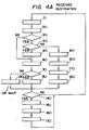
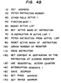
- Fig. 4A A description will be given, with reference to the flow-chart of Figs. 4A & 4B of the operation of the embodiment shown in Fig. 3.
- the reference numbers in Fig. 4A refer to the list of Fig. 4B.
- step 10 in Fig. 4A indicates a SET ADDRESS process (Fig. 4B).
- Fig. 5 shows an example of a timing chart of the execution of an instruction according to the present invention.
- a time slot T an instruction is fetched; in a time slot T 2 , the instruction is decoded; in a time slot T 3 , it is checked whether the instruction is executable, and the register number is assigned; in a time slot T 4 , the instruction is issued to the operation unit 7; in time slots T 5 to T 8 , operation specified by the instruction is executed; in the time slot T 8 , an address based on the content of the destination field of the instruction is set in the address register of the instruction memory 2; and in a time slot Tg, the next instruction is fetched which is linked with the instruction executed.
- one of two next instructions is fetched on the basis of the content of a first one of two destination fields and then the other next instruction is fetched on the basis of the content of the second destination field.
- the instructions 2 to 5 are processed one after another in a pipeline fashion as shown in Fig. 5.
- a plurality of operators in the operation unit 7 need not always be synchronized in operation but the pipelines may also operate in parallel and asynchronously.
- the above data register can easily be applied to vector processing, too, in which a plurality of data (vector data) are all stored in one register and a plurality of the same operations are executed on these data at a time.
- Scalar processing which processes a single data can also be simplified by considering that it is a special case of handling a single data in the vector processing.
- the register number When the register number are assigned, they may sometimes exceed the number of registers that hardware has, causing a deadlock. This can be avoided by a system in which program execution is limited by software within a range in which the register numbers do not exceed a specified number of registers, or a system in which the data is saved by hardware into a memory or another register, thereby to release the data register from the busy state.
- Figs. 6 and 7 show the hardware structure of another embodiment of the present invention and a timing chart of the execution of an instruction in the embodiment, respectively. Circled reference signs below refer to Fig. 2A and Fig. 7.
- An instruction group is preset by an external control circuit in an instruction memory 21. Upon application of external data, an address is set in an address register 11 and the instruction 1 is read out from instruction memory 21 and set in an instruction register 15. Thereafter the external data is applied from an input 26 and provided via registers 18 and 19 to a data memory 22. The address of the location in the data memory 22 is supplied from an address register 16 via registers 13 and 14.
- the instruction read out into the instruction register 15 is an external set instruction
- the instruction 2 is read out on the basis of the content of its destination field (that is, the R1 part of the instruction 2 .
- the instruction 2 set in the instruction register 15 cannot be executed because its R2 part is not active. Then the operation shifts to processing of the instruction 3 resulting from the arrival of external data.
- the data entered from the input 26 is provided to the register 18.
- the destination of the instruction @ is the R2 part of the instruction 2 and the instruction 2 has already been stored in the instruction register 15 until then. Since its R1 part is active, the instruction 2 is executable. Then the instruction 2 is provided to an operator 23 via the register 18.
- the instruction 4 is a two-brach instruction and, consequently, data @ and @ and written into the data memory 22 at addresses corresponding to the instructions 5 and 6, respectively.
- the instructions 2, @ and @ are written into the data memory 22 via a route [address register 11-register 13 ⁇ register 14 ⁇ address register 16]. Since the data is the same as the result of execution of the instruction 2, the same data as the instruction @ is held in the registers 18 and 19.
- the instructions 5 and @ are linked with the next instructions and the processing therefor is performed in the same way as mentioned above; hence no description will be given thereof.
- the number of words of the instruction memory and the data memory are selected to be the same, data does not overflow.
- the addresses of the instruction memory and the data memory have one-to-one correspondence.
- the number of words of the data memory may be smaller than the number of words of the instruction memory but, in such a case, an address converter or associative storage is needed.
- the execution of an instruction is performed in one cycle; but, if several cycles are required for the execution of an instruction, an instruction fetch must be delayed for several cycles correspondingly.
- Registers 24 and 25 may carry the instruction code of an instruction set in the instruction register 15 to the operator 23 to determine the operation to be effected.
- Address register part 12 and the illustrated ⁇ (+1) counter may be for address incrementing (or decrementing).
Landscapes
- Engineering & Computer Science (AREA)
- Software Systems (AREA)
- Theoretical Computer Science (AREA)
- Physics & Mathematics (AREA)
- General Engineering & Computer Science (AREA)
- General Physics & Mathematics (AREA)
- Advance Control (AREA)
Description
- The present invention relates to an information processing unit and, more particularly, to a data flow type information processing unit.
- In a Von Neumann type information processing unit, the execution of an instruction is subject to what is called sequential control but, in a data flow type information processing unit, an instruction can be executed when data necessary therefor is available and the sequence of the execution of instructions can be freely determined by hardware and, further, a plurality of instructions can be executed in parallel. Therefore, a data flow type information processing unit is effective, for example, for the implementation of a vector processor which executes vector instructions in parallel.
- However, the application of the configuration of a conventional data flow type information processing unit to an information processing unit for scientific computations encounters various problems. A major one of the problems is that, in the conventional data flow type information processing unit, an instruction and data (values) are mixed into one packet for transfer. On account of this, in the conventional data flow type information processing unit, a hardware circuit for moving an instruction and a circuit for transferring data cannot be separated, which offsets one of the advantages that break what is called the Von Neumann bottleneck.
- US-A-3 962 706 discloses such an information processing unit. This information processing unit is one which makes an instruction executable on the basis of the determination that operand data necessary for executing the instruction becomes or will become effective and properly executes the instruction by hardware, and in which a first instruction has an operation code field, an input field having a sufficient number of bits to indicate whether the operand data to be used by the first instruction is active or non-active, and a destination field for specifying the input field of a second instruction to be linked with the first instruction, and the first instruction is arranged so that when it is executed, it is indicated in the input field of the second instruction specified by the destination field of the first instruction that the operand data for the second instruction is active, the information processing unit comprising:- an instruction memory for storing the instructions; a data memory for storing the operand data; an instruction fetch part for fetching an executable instruction or instructions from the instruction memory; and an operation unit for loading desired operand data from the data memory to execute the fetched instruction or instructions in parallel.
- An embodiment of the present invention can provide an information processing unit which performs instruction processing on the basis of the dependency of an instruction on data and in which paths for the instruction and the data are separated and the data is transferred in dependence upon instruction flow.
- An embodiment of the present invention can provide an information processing unit in which a desired one of instructions is determined on the basis of a proper sequence and a register number assign circuit automatically assigns to the instruction a register in which to place the processing result by hardware processing, and the software side is required only to provide a data flow control.
- An embodiment of the present invention can provide an information processing unit in which register numbers are prepared corresponding to instructions, thereby to permit identification of data.
- An embodiment of the present invention can provide an information processing unit in which when an instruction is issued to an operation unit, the content of an input field of the instruction is cleared to make it non-active, enabling the instruction to be utilized as the next instruction.
- According to the present invention, there is provided an information processing unit which makes an instruction executable on the basis of determination that operand data necessary for executing the instruction becomes or will become effective and properly executes the instruction by hardware, and in which a first instruction has an operation code field, an input field having a sufficient number of bits to indicate whether the operand data to be used by the first instruction is active or non-active, and a destination field for specifying the input field of a second instruction to be linked with the first instruction and the first instruction is arranged so that when it is executed, it is indicated in the input field of the second instruction specified by the destination field of the first instruction that operand data for the second instruction is active, the information processing unit comprising:
- an instruction memory for storing the instructions;
- a data memory for storing the operand data;
- an instruction fetch part for fetching an executable instruction or instructions from the instruction memory; and
- an operation unit for loading desired operand data from the data memory to execute the fetched instruction or instructions in parallel, characterised in that
- the instruction memory and the data memory are separate, and in that data and instructions follow separate paths in the processing unit.
- An embodiment of the present invention can provide a data flow type information processing unit arranged so that an input field of an instruction is given information indicating whether operand data to be used by the instruction has already been made active, and that the operand data is transferred in dependence on control corresponding to an instruction.
- Reference is made, by way of example, to the accompanying drawings, in which:-
- Figs. 1A and 1B are schematic diagrams showing examples of instruction formats for use in embodiments of the present invention;
- Figs. 2A and 2B are schematic diagrams explanatory of linkage of instructions according to embodiments of the present invention;
- Fig. 3 is a block diagram illustrating the hardware arrangement of an embodiment of the present invention;
- Fig. 4A is a flowchart, and Fig. 4B is an associated list, explanatory of an instruction processing operation in an embodiment of the present invention;
- Fig. 5 is a timing chart explanatory of execution of an instruction in the embodiment shown in Fig. 3;
- Fig. 6 is a block diagram illustrating the hardware arrangement of another embodiment of the present invention; and
- Fig. 7 is a timing chart explanatory of the execution of an instruction in the embodiment shown in Fig. 6.
- In embodiments of the present invention, instructions related to operations have such an instruction format as shown in Fig. 1A which comprises an instruction code (OP) field, two input fields (R,, R2), and a destination field (D). In the format of Fig. 1A, M is a field not related to the present invention and so not described. On the other hand, instructions related to control, such as copy, switch and union, have such an instruction format as shown in Fig. 1B which comprises an instruction code (OP) field, an input field (Ri) and two destination fields (Di, D2). The input field and the destination field need not always be one or two in number but may also be three or more in number.
- Now, assuming such graph type instruction control linkage as shown in Fig. 2A in which "
instructions 1 and 3 are first executed to make annstruction 2 executable and than an instruction @ is executed to makeinstructions instruction 2 specified by the destination field D of the instruction 1 indicating that one of the operand data to be used by theinstruction 2 has become active. Similarly, by the determination that operand data becomes or will become active as a result of the execution of theinstruction 3, a certain value is set in the input field R2 of theinstruction 2 specified by the destination field D of theinstruction 3, indicating that another one of the operand data to be used by theinstruction 2 has become active. And, by completion of the execution of theinstruction 2, a certain value is set in the input field R, of the instruction @ specified by the destination field D of theinstruction 2, indicating that the instruction @ has become executable. Likewise, by completion of the execution of the instruction @, values are set in the input fields of theinstructions instruction 4 is linked with theinstructions 5 and @. - In the case of the present invention, it is sufficient theoretically that the input field shown in Figs. 1A and 1B is a 1-bit field (indicating that the operand data has becomes active), but it is preferable that the input field be of an 8-bit field length, as shown in Figs. 1A and 1B, to permit writing therein the number of register in which the operand data is being set, thereby indicating that the operand data has become active, coupled with writing of the register number where the data is located.
- Incidentally, the instructions for use in the present invention are (i) arithmetic operations, such as ADD, MULTIPLY, DIVIDE and so forth, (ii) ordinary instructions, such as COMPARE, LOGICAL, SHIFT, MASKLOGICAL, LOAD, STORE and so forth, (iii) control instructions, such as COPY, SWITCH, UNION and so forth, (iv) function link instructions, such as APPLY and so on, and (v) interface instruction for external part, such as input/output. It is also possible that these instructions are each provided both as a vector instruction and as a scalar instruction, if necessary.
- Fig. 3 illustrates the hardware structure of an embodiment of the present invention. In Fig. 3, reference numeral 1 indicates an interface for external parts; 2 designates an instruction memory having stored therein such instructions as shown in Figs. 1A and 1B; 3 identifies a data memory having stored therein operand data; 4 denotes a memory controller which performs processing of accessing the
data memory 3 to load desired operand data in a register of the register number specified by the contents of the input fields R, and R2 or restoring operation results in thedata memory 3; 5 represents an instruction fetch part which checks whether instructions read out from theinstruction memory 2 are executable and fetches the executable instruction; and 6 shows a register number assign circuit in which, when resources to be used by an executable instruction, such as an operator (an operation unit), a register and so forth, are usable, and it is determined to issue the instruction, assigns the number of a register for storing a destination operand of the instruction automatically in hardware. The assigned register number is provided to the instruction fetch part, which writes the register number into the input field of another instruction specified by the destination field of the abovesaid instruction.Reference numeral 7 refers to an operation unit, which comprises one or a plurality of operation parts which execute a desired operation; 8 signifies a register group; and 9 indicates an active instruction list part, in which executable but queued instructions are held in the form of a list. The abovesaid data memory and instruction memory may also be physically the same memory. - A description will be given, with reference to the flow-chart of Figs. 4A & 4B of the operation of the embodiment shown in Fig. 3. The reference numbers in Fig. 4A refer to the list of Fig. 4B. For example,
step 10 in Fig. 4A indicates a SET ADDRESS process (Fig. 4B). - (A) The interface for external parts 1 has interfaces with a central processing unit, an input/ output device and so on, and performs processing of transferring data between other devices and the
data memory 3. Furthermore, it performs processing of writing an instruction into theinstruction memory 2 as required. - (B) Now, let it bs assumed that it is determined that the execution of an instruction is completed or will be complete. In this state, address information based on the content of the destination field of the instruction is set in an address register for the instruction memory 2 (
step 10, SET ADDRESS). - (C) By this, one instruction is fetched from the instruction memory 2 (
step 20, FETCH INSTRUCTION MEMORY). - (D) If the fetched instruction contains an input field which requires a result of another instruction, the instruction fetch
part 5 checks whether the fetched instruction's input field is active (step 30, OTHER FIELD ACTIVE P). - (E) If the input field is not active, an already assigned register number is written into the input field specified by the destination field and the fetched instruction is returned to the instruction memory 2 (
step 60, SET ACTIVE MARK AT INSTRUCTION). - (F) If the input field is active, the register number is assigned and the execution of the instruction is started. At this time, however, if a desired operation unit or the like is busy (
step 40, FUNCTION BUSY ?), address information representing the instruction is registered in the active instruction list part 9 (step 50, REGIST ACTIVE LIST) and the assigned register number is written into the input field of that one of the instructions in theinstruction memory 2 which is specified by the destination field of the instruction (step 60, SET ACTIVE MARK AT INSTRUCTION). - (G) If another instruction has been registered in the active instruction list part 9 (
step 70, IS INSTRUCTION IN ACTIVE LIST ?), then it is fetched from theinstruction memory 2 for execution next (step 80, FETCH INSTRUCTION FROM ACTIVE LIST). In the event that another instruction has not been registered in the activeinstruction list part 9, theinstruction memory 2 is accessed, for instance, in accordance with the content of a sequential memory in search for an active instruction (step 130, USE SEQUENTIAL ACCESS COUNTER). Of course, the activeinstruction list part 9 may be dispensed with and, in such a case, an executable instruction is executed after the desired operation unit or the like is released from the busy state but the accuracy of parallel execution of instructions is decreased, resulting in impaired performance. - (H) Going back to the steps followed after
step 40, when the desired operation part or the like is not busy, and if only processing as mentioned above in (F) is performed, the instruction is left in the executable state. To avoid this, the instruction fetchpart 5 clears the content of the input field of the fetched instruction and rewrites it into theinstruction memory 2 on the assumption that it is determined that the instruction is completed or will be completed (step 90, RESET ACTIVE MARK OF INSTRUCTION). - (I) The register number assign
circuit 6 determines, by hardware processing, the register number to be written into the input field of an instruction specified by the destination field (step 100, ASSIGN NUMBER OF REGISTER) and then issues an instruction to the operation unit 7 (step 110, ISSUE INSTRUCTION). - (J) On the other hand, the instruction fetch
part 5 sets the content of the abovesaid destination field in an address register (not shown) of the instruction memory 2 (step 120). - (K) In the operation unit 7 a plurality of instruction usually run in parallel.
- (L) When an interrupt occurs (
step 140, INTERRUPTION GENERATE ?), for instance a fixed address is produced (step 160, SET FIXED ADDRESS afterstep 150, SAVE ADDRESS) as in the case of the conventional data flow type information processing unit and an interrupt- servicing program which starts with an instruction stored at that fixed address is executed. - (M) Upon completion of a certain instruction, the
operation unit 7 sets the operation results in a register predetermined by the register number assigne circuit 6 (step 170, SET SAVED ADDRESS). In the above, if a plurality of interrupt conditions are present when setting the address register of theinstruction memory 2, then an address of an appropriate interrupt servicing program is set using a priority circuit. - Fig. 5 shows an example of a timing chart of the execution of an instruction according to the present invention. In a time slot T" an instruction is fetched; in a time slot T2, the instruction is decoded; in a time slot T3, it is checked whether the instruction is executable, and the register number is assigned; in a time slot T4, the instruction is issued to the
operation unit 7; in time slots T5 to T8, operation specified by the instruction is executed; in the time slot T8, an address based on the content of the destination field of the instruction is set in the address register of theinstruction memory 2; and in a time slot Tg, the next instruction is fetched which is linked with the instruction executed. When the operation unit happens to be busy (in time slot T3), the instruction is registered in the activeinstruction list part 9 in the time slot T4 and processing of fetching another instruction from the activeinstruction list part 9 takes place in the time slot Ts and, in the time slot Ts, the address setting is performed. - In the case where the instruction contains two destination fields, one of two next instructions is fetched on the basis of the content of a first one of two destination fields and then the other next instruction is fetched on the basis of the content of the second destination field. The
instructions 2 to 5 are processed one after another in a pipeline fashion as shown in Fig. 5. - In the present invention, for example, a plurality of operators in the
operation unit 7 need not always be synchronized in operation but the pipelines may also operate in parallel and asynchronously. - The above data register can easily be applied to vector processing, too, in which a plurality of data (vector data) are all stored in one register and a plurality of the same operations are executed on these data at a time. Scalar processing which processes a single data can also be simplified by considering that it is a special case of handling a single data in the vector processing. When the register number are assigned, they may sometimes exceed the number of registers that hardware has, causing a deadlock. This can be avoided by a system in which program execution is limited by software within a range in which the register numbers do not exceed a specified number of registers, or a system in which the data is saved by hardware into a memory or another register, thereby to release the data register from the busy state.
- Figs. 6 and 7 show the hardware structure of another embodiment of the present invention and a timing chart of the execution of an instruction in the embodiment, respectively. Circled reference signs below refer to Fig. 2A and Fig. 7. An instruction group is preset by an external control circuit in an
instruction memory 21. Upon application of external data, an address is set in anaddress register 11 and the instruction 1 is read out frominstruction memory 21 and set in aninstruction register 15. Thereafter the external data is applied from aninput 26 and provided viaregisters data memory 22. The address of the location in thedata memory 22 is supplied from anaddress register 16 viaregisters instruction register 15 is an external set instruction, theinstruction 2 is read out on the basis of the content of its destination field (that is, the R1 part of theinstruction 2 . Theinstruction 2 set in theinstruction register 15 cannot be executed because its R2 part is not active. Then the operation shifts to processing of theinstruction 3 resulting from the arrival of external data. The data entered from theinput 26 is provided to theregister 18. The destination of the instruction @ is the R2 part of theinstruction 2 and theinstruction 2 has already been stored in theinstruction register 15 until then. Since its R1 part is active, theinstruction 2 is executable. Then theinstruction 2 is provided to anoperator 23 via theregister 18. At this time, data corresponding to the R1 part is read out from thedata memory 22 by the address of theaddress register 16 based on theinstruction 2 stored in theinstruction register 15 and the data thus read out is provided to theregister 17, from which it is applied to theoperator 23 together with the abovesaid data stored in theregister 18. As a result of this, the instruction @ is executed and the execution result is applied to theregister 18. The output of theregister 18 is provided to theregister 19 and, at this time, the destination of theinstruction 2 sent via theregisters address register 16 to thedata memory 22, by which the result of execution of theinstruction 2 in theregister 19 is written into thedata memory 22. Since the destination of theinstruction 2 is @ the abovesaid execution result is written into thedata memory 22 at an address corresponding to the instruction @. Theinstruction 4 is a two-brach instruction and, consequently, data @ and @ and written into thedata memory 22 at addresses corresponding to theinstructions instructions 2, @ and @ are written into thedata memory 22 via a route [address register 11-register 13→register 14→address register 16]. Since the data is the same as the result of execution of theinstruction 2, the same data as the instruction @ is held in theregisters instructions 5 and @ are linked with the next instructions and the processing therefor is performed in the same way as mentioned above; hence no description will be given thereof. In the above, if the number of words of the instruction memory and the data memory are selected to be the same, data does not overflow. The addresses of the instruction memory and the data memory have one-to-one correspondence. Incidentally, since the data memory is not used in some cases, the number of words of the data memory may be smaller than the number of words of the instruction memory but, in such a case, an address converter or associative storage is needed. In the timing chart of Fig. 7 the execution of an instruction is performed in one cycle; but, if several cycles are required for the execution of an instruction, an instruction fetch must be delayed for several cycles correspondingly. -
Registers instruction register 15 to theoperator 23 to determine the operation to be effected. -
Address register part 12 and the illustrated ± (+1) counter may be for address incrementing (or decrementing).
Claims (6)
characterised in that
Applications Claiming Priority (2)
| Application Number | Priority Date | Filing Date | Title |
|---|---|---|---|
| JP33435/82 | 1982-03-03 | ||
| JP57033435A JPS58151655A (en) | 1982-03-03 | 1982-03-03 | Information processing device |
Publications (3)
| Publication Number | Publication Date |
|---|---|
| EP0087978A2 EP0087978A2 (en) | 1983-09-07 |
| EP0087978A3 EP0087978A3 (en) | 1985-07-31 |
| EP0087978B1 true EP0087978B1 (en) | 1989-05-10 |
Family
ID=12386450
Family Applications (1)
| Application Number | Title | Priority Date | Filing Date |
|---|---|---|---|
| EP83301103A Expired EP0087978B1 (en) | 1982-03-03 | 1983-03-02 | Information processing unit |
Country Status (7)
| Country | Link |
|---|---|
| US (1) | US4675806A (en) |
| EP (1) | EP0087978B1 (en) |
| JP (1) | JPS58151655A (en) |
| BR (1) | BR8301016A (en) |
| CA (1) | CA1204516A (en) |
| DE (1) | DE3379850D1 (en) |
| ES (1) | ES8402954A1 (en) |
Families Citing this family (53)
| Publication number | Priority date | Publication date | Assignee | Title |
|---|---|---|---|---|
| USRE34052E (en) * | 1984-05-31 | 1992-09-01 | International Business Machines Corporation | Data processing system with CPU register to register data transfers overlapped with data transfer to and from main storage |
| US5206945A (en) * | 1985-03-15 | 1993-04-27 | Hitachi, Ltd. | Single-chip pipeline processor for fetching/flushing instruction/data caches in response to first/second hit/mishit signal respectively detected in corresponding to their logical addresses |
| JP2539357B2 (en) | 1985-03-15 | 1996-10-02 | 株式会社日立製作所 | Data processing device |
| US4972314A (en) * | 1985-05-20 | 1990-11-20 | Hughes Aircraft Company | Data flow signal processor method and apparatus |
| JPH0632056B2 (en) * | 1985-05-31 | 1994-04-27 | 松下電器産業株式会社 | Data processing device |
| JPH0766329B2 (en) * | 1985-06-14 | 1995-07-19 | 株式会社日立製作所 | Information processing equipment |
| US5349672A (en) * | 1986-03-17 | 1994-09-20 | Hitachi, Ltd. | Data processor having logical address memories and purge capabilities |
| EP0239081B1 (en) * | 1986-03-26 | 1995-09-06 | Hitachi, Ltd. | Pipelined data processor capable of decoding and executing plural instructions in parallel |
| US4814978A (en) * | 1986-07-15 | 1989-03-21 | Dataflow Computer Corporation | Dataflow processing element, multiprocessor, and processes |
| US4980824A (en) * | 1986-10-29 | 1990-12-25 | United Technologies Corporation | Event driven executive |
| US4811215A (en) * | 1986-12-12 | 1989-03-07 | Intergraph Corporation | Instruction execution accelerator for a pipelined digital machine with virtual memory |
| US5001624A (en) * | 1987-02-13 | 1991-03-19 | Harrell Hoffman | Processor controlled DMA controller for transferring instruction and data from memory to coprocessor |
| US4972315A (en) * | 1987-03-10 | 1990-11-20 | Mitsubishi Denki Kabushiki Kaisha | Data flow machine |
| JPH0192851A (en) * | 1987-10-02 | 1989-04-12 | Hitachi Ltd | Address space switching device |
| JPH0646414B2 (en) * | 1987-10-20 | 1994-06-15 | シャープ株式会社 | Information processing equipment |
| US5115510A (en) * | 1987-10-20 | 1992-05-19 | Sharp Kabushiki Kaisha | Multistage data flow processor with instruction packet, fetch, storage transmission and address generation controlled by destination information |
| US5117499A (en) * | 1988-01-22 | 1992-05-26 | Sharp Kabushiki Kaisha | Data flow type processing apparatus having external and cache memories for fetching paired executing instruction when mishit occurs |
| JPH01188951A (en) * | 1988-01-23 | 1989-07-28 | Sharp Corp | Control system for execution of data flow program |
| JPH06101044B2 (en) * | 1988-01-23 | 1994-12-12 | シャープ株式会社 | Deadlock avoidance execution control method |
| US5125097A (en) * | 1988-01-29 | 1992-06-23 | Sharp Kabushiki Kaisha | Data flow type information processors where data packets pass through plurality of merging and branching portions of the internal path |
| US4974146A (en) * | 1988-05-06 | 1990-11-27 | Science Applications International Corporation | Array processor |
| US5513332A (en) * | 1988-05-31 | 1996-04-30 | Extended Systems, Inc. | Database management coprocessor for on-the-fly providing data from disk media to all without first storing data in memory therebetween |
| JPH03500461A (en) * | 1988-07-22 | 1991-01-31 | アメリカ合衆国 | Data flow device for data-driven calculations |
| US5163142A (en) * | 1988-10-28 | 1992-11-10 | Hewlett-Packard Company | Efficient cache write technique through deferred tag modification |
| US5241635A (en) * | 1988-11-18 | 1993-08-31 | Massachusetts Institute Of Technology | Tagged token data processing system with operand matching in activation frames |
| US5689647A (en) * | 1989-03-14 | 1997-11-18 | Sanyo Electric Co., Ltd. | Parallel computing system with processing element number setting mode and shortest route determination with matrix size information |
| US5487156A (en) * | 1989-12-15 | 1996-01-23 | Popescu; Valeri | Processor architecture having independently fetching issuing and updating operations of instructions which are sequentially assigned and stored in order fetched |
| US5150470A (en) * | 1989-12-20 | 1992-09-22 | International Business Machines Corporation | Data processing system with instruction queue having tags indicating outstanding data status |
| USRE35311E (en) * | 1990-04-04 | 1996-08-06 | International Business Machines Corporation | Data dependency collapsing hardware apparatus |
| US5404553A (en) * | 1991-01-09 | 1995-04-04 | Mitsubishi Denki Kabushiki Kaisha | Microprocessor and data flow microprocessor having vector operation function |
| US5493687A (en) | 1991-07-08 | 1996-02-20 | Seiko Epson Corporation | RISC microprocessor architecture implementing multiple typed register sets |
| DE69231762T2 (en) * | 1991-07-08 | 2001-07-26 | Seiko Epson Corp., Tokio/Tokyo | RISC PROCESSOR WITH EXTENDABLE ARCHITECTURE |
| US5539911A (en) | 1991-07-08 | 1996-07-23 | Seiko Epson Corporation | High-performance, superscalar-based computer system with out-of-order instruction execution |
| US5961629A (en) * | 1991-07-08 | 1999-10-05 | Seiko Epson Corporation | High performance, superscalar-based computer system with out-of-order instruction execution |
| US5423040A (en) * | 1991-07-24 | 1995-06-06 | International Business Machines Corporation | System and method for efficiently executing directed acyclic graphs |
| US5363495A (en) * | 1991-08-26 | 1994-11-08 | International Business Machines Corporation | Data processing system with multiple execution units capable of executing instructions out of sequence |
| EP0544083A3 (en) * | 1991-11-26 | 1994-09-14 | Ibm | Interleaved risc-type parallel processor and processing methods |
| US5438668A (en) * | 1992-03-31 | 1995-08-01 | Seiko Epson Corporation | System and method for extraction, alignment and decoding of CISC instructions into a nano-instruction bucket for execution by a RISC computer |
| DE69311330T2 (en) | 1992-03-31 | 1997-09-25 | Seiko Epson Corp., Tokio/Tokyo | COMMAND SEQUENCE PLANNING FROM A RISC SUPER SCALAR PROCESSOR |
| WO1993022722A1 (en) | 1992-05-01 | 1993-11-11 | Seiko Epson Corporation | A system and method for retiring instructions in a superscalar microprocessor |
| US5636150A (en) * | 1992-08-06 | 1997-06-03 | Sharp Kabushiki Kaisha | Data driven type digital filter unit and data driven type information processor including the same |
| US6735685B1 (en) * | 1992-09-29 | 2004-05-11 | Seiko Epson Corporation | System and method for handling load and/or store operations in a superscalar microprocessor |
| DE69329778T2 (en) | 1992-09-29 | 2001-04-26 | Seiko Epson Corp., Tokio/Tokyo | SYSTEM AND METHOD FOR HANDLING LOADS AND / OR STORES IN A SUPER-SCALAR MICROPROCESSOR |
| US5628021A (en) * | 1992-12-31 | 1997-05-06 | Seiko Epson Corporation | System and method for assigning tags to control instruction processing in a superscalar processor |
| EP1107111A3 (en) * | 1992-12-31 | 2002-02-06 | Seiko Epson Corporation | System and method for register renaming |
| CA2123442A1 (en) * | 1993-09-20 | 1995-03-21 | David S. Ray | Multiple execution unit dispatch with instruction dependency |
| US5765014A (en) * | 1993-10-12 | 1998-06-09 | Seki; Hajime | Electronic computer system and processor element for processing in a data driven manner using reverse polish notation |
| GB2289664B (en) * | 1994-05-27 | 1998-04-29 | Instance Ltd David J | Labels and manufacture thereof |
| US5826072A (en) * | 1995-11-13 | 1998-10-20 | Oasis Design, Inc. | Pipelined digital signal processor and signal processing system employing same |
| US6092184A (en) * | 1995-12-28 | 2000-07-18 | Intel Corporation | Parallel processing of pipelined instructions having register dependencies |
| US5974538A (en) * | 1997-02-21 | 1999-10-26 | Wilmot, Ii; Richard Byron | Method and apparatus for annotating operands in a computer system with source instruction identifiers |
| RU2130198C1 (en) * | 1997-08-06 | 1999-05-10 | Бурцев Всеволод Сергеевич | Computer |
| US6553483B1 (en) * | 1999-11-29 | 2003-04-22 | Intel Corporation | Enhanced virtual renaming scheme and deadlock prevention therefor |
Family Cites Families (8)
| Publication number | Priority date | Publication date | Assignee | Title |
|---|---|---|---|---|
| NL7004570A (en) * | 1970-03-31 | 1971-10-04 | ||
| BE789583A (en) * | 1971-10-01 | 1973-02-01 | Sanders Associates Inc | PROGRAM CONTROL APPARATUS FOR DATA PROCESSING MACHINE |
| GB1443777A (en) * | 1973-07-19 | 1976-07-28 | Int Computers Ltd | Data processing apparatus |
| US4025771A (en) * | 1974-03-25 | 1977-05-24 | Hughes Aircraft Company | Pipe line high speed signal processor |
| US3962706A (en) * | 1974-03-29 | 1976-06-08 | Massachusetts Institute Of Technology | Data processing apparatus for highly parallel execution of stored programs |
| US4168523A (en) * | 1975-11-07 | 1979-09-18 | Ncr Corporation | Data processor utilizing a two level microaddressing controller |
| US4153941A (en) * | 1976-11-11 | 1979-05-08 | Kearney & Trecker Corporation | Timing circuit and method for controlling the operation of cyclical devices |
| US4366536A (en) * | 1980-04-15 | 1982-12-28 | National Semiconductor Corporation | Modular digital computer system for storing and selecting data processing procedures and data |
-
1982
- 1982-03-03 JP JP57033435A patent/JPS58151655A/en active Pending
-
1983
- 1983-03-01 ES ES520203A patent/ES8402954A1/en not_active Expired
- 1983-03-02 DE DE8383301103T patent/DE3379850D1/en not_active Expired
- 1983-03-02 US US06/471,524 patent/US4675806A/en not_active Expired - Lifetime
- 1983-03-02 EP EP83301103A patent/EP0087978B1/en not_active Expired
- 1983-03-02 CA CA000422734A patent/CA1204516A/en not_active Expired
- 1983-03-02 BR BR8301016A patent/BR8301016A/en not_active IP Right Cessation
Also Published As
| Publication number | Publication date |
|---|---|
| EP0087978A2 (en) | 1983-09-07 |
| ES520203A0 (en) | 1984-03-01 |
| DE3379850D1 (en) | 1989-06-15 |
| ES8402954A1 (en) | 1984-03-01 |
| CA1204516A (en) | 1986-05-13 |
| JPS58151655A (en) | 1983-09-08 |
| EP0087978A3 (en) | 1985-07-31 |
| US4675806A (en) | 1987-06-23 |
| BR8301016A (en) | 1983-11-22 |
Similar Documents
| Publication | Publication Date | Title |
|---|---|---|
| EP0087978A2 (en) | Information processing unit | |
| EP0061096B1 (en) | Data processing system for parallel processing | |
| EP0487082B1 (en) | Nesting management mechanism for use in loop control system | |
| US5251306A (en) | Apparatus for controlling execution of a program in a computing device | |
| US5218712A (en) | Providing a data processor with a user-mode accessible mode of operations in which the processor performs processing operations without interruption | |
| US5341482A (en) | Method for synchronization of arithmetic exceptions in central processing units having pipelined execution units simultaneously executing instructions | |
| US5442757A (en) | Computer processor with distributed pipeline control that allows functional units to complete operations out of order while maintaining precise interrupts | |
| CA1214566A (en) | Method of synchronizing the sequence by which a variety of randomly called unrelated activities are executed in a digital processor | |
| EP0213842A2 (en) | Mechanism for performing data references to storage in parallel with instruction execution on a reduced instruction-set processor | |
| EP0476722B1 (en) | Data processing system | |
| EP0335514A2 (en) | Exception reporting mechanism for a vector processor | |
| JPH0766329B2 (en) | Information processing equipment | |
| US3654621A (en) | Information processing system having means for dynamic memory address preparation | |
| US4780820A (en) | Control flow computer using mode and node driving registers for dynamically switching between parallel processing and emulation of von neuman processors | |
| US4152763A (en) | Control system for central processing unit with plural execution units | |
| JPS6334490B2 (en) | ||
| JPS6142308B2 (en) | ||
| JPH0461390B2 (en) | ||
| AU626263B2 (en) | Apparatus and method for providing an extended processing environment on nonmicrocoded data processing system | |
| EP0105125B1 (en) | Data processing system | |
| JPS6236575B2 (en) | ||
| JP2814683B2 (en) | Instruction processing unit | |
| JP2000029703A (en) | Dsp architecture optimized for memory access | |
| KR880001399B1 (en) | Data processor | |
| JPS59218569A (en) | micro computer |
Legal Events
| Date | Code | Title | Description |
|---|---|---|---|
| PUAI | Public reference made under article 153(3) epc to a published international application that has entered the european phase |
Free format text: ORIGINAL CODE: 0009012 |
|
| AK | Designated contracting states |
Designated state(s): DE FR GB |
|
| PUAL | Search report despatched |
Free format text: ORIGINAL CODE: 0009013 |
|
| AK | Designated contracting states |
Designated state(s): DE FR GB |
|
| 17P | Request for examination filed |
Effective date: 19851125 |
|
| 17Q | First examination report despatched |
Effective date: 19861215 |
|
| GRAA | (expected) grant |
Free format text: ORIGINAL CODE: 0009210 |
|
| AK | Designated contracting states |
Kind code of ref document: B1 Designated state(s): DE FR GB |
|
| REF | Corresponds to: |
Ref document number: 3379850 Country of ref document: DE Date of ref document: 19890615 |
|
| ET | Fr: translation filed | ||
| PLBI | Opposition filed |
Free format text: ORIGINAL CODE: 0009260 |
|
| 26 | Opposition filed |
Opponent name: N.V. PHILIPS' GLOEILAMPENFABRIEKEN Effective date: 19900212 |
|
| PLBN | Opposition rejected |
Free format text: ORIGINAL CODE: 0009273 |
|
| STAA | Information on the status of an ep patent application or granted ep patent |
Free format text: STATUS: OPPOSITION REJECTED |
|
| 27O | Opposition rejected |
Effective date: 19910125 |
|
| PGFP | Annual fee paid to national office [announced via postgrant information from national office to epo] |
Ref country code: GB Payment date: 19990304 Year of fee payment: 17 |
|
| PGFP | Annual fee paid to national office [announced via postgrant information from national office to epo] |
Ref country code: DE Payment date: 19990305 Year of fee payment: 17 |
|
| PGFP | Annual fee paid to national office [announced via postgrant information from national office to epo] |
Ref country code: FR Payment date: 19990309 Year of fee payment: 17 |
|
| PG25 | Lapsed in a contracting state [announced via postgrant information from national office to epo] |
Ref country code: GB Free format text: LAPSE BECAUSE OF NON-PAYMENT OF DUE FEES Effective date: 20000302 |
|
| GBPC | Gb: european patent ceased through non-payment of renewal fee |
Effective date: 20000302 |
|
| PG25 | Lapsed in a contracting state [announced via postgrant information from national office to epo] |
Ref country code: FR Free format text: LAPSE BECAUSE OF NON-PAYMENT OF DUE FEES Effective date: 20001130 |
|
| REG | Reference to a national code |
Ref country code: FR Ref legal event code: ST |
|
| PG25 | Lapsed in a contracting state [announced via postgrant information from national office to epo] |
Ref country code: DE Free format text: LAPSE BECAUSE OF NON-PAYMENT OF DUE FEES Effective date: 20010103 |