EP0121096B1 - Structure de contact pour semi-conducteur - Google Patents
Structure de contact pour semi-conducteur Download PDFInfo
- Publication number
- EP0121096B1 EP0121096B1 EP84102100A EP84102100A EP0121096B1 EP 0121096 B1 EP0121096 B1 EP 0121096B1 EP 84102100 A EP84102100 A EP 84102100A EP 84102100 A EP84102100 A EP 84102100A EP 0121096 B1 EP0121096 B1 EP 0121096B1
- Authority
- EP
- European Patent Office
- Prior art keywords
- region
- source
- fet
- conductivity type
- semiconductor
- Prior art date
- Legal status (The legal status is an assumption and is not a legal conclusion. Google has not performed a legal analysis and makes no representation as to the accuracy of the status listed.)
- Expired
Links
- 239000004065 semiconductor Substances 0.000 title claims description 37
- 230000003071 parasitic effect Effects 0.000 claims description 21
- 229910052710 silicon Inorganic materials 0.000 claims description 6
- 239000010703 silicon Substances 0.000 claims description 6
- 230000000295 complement effect Effects 0.000 claims description 5
- 239000002019 doping agent Substances 0.000 claims description 5
- 230000005641 tunneling Effects 0.000 claims description 4
- 238000012546 transfer Methods 0.000 claims description 2
- 230000000694 effects Effects 0.000 description 7
- 239000000758 substrate Substances 0.000 description 7
- XUIMIQQOPSSXEZ-UHFFFAOYSA-N Silicon Chemical compound [Si] XUIMIQQOPSSXEZ-UHFFFAOYSA-N 0.000 description 5
- 230000004888 barrier function Effects 0.000 description 4
- 238000002347 injection Methods 0.000 description 4
- 239000007924 injection Substances 0.000 description 4
- 238000000034 method Methods 0.000 description 4
- 238000005513 bias potential Methods 0.000 description 3
- 230000009471 action Effects 0.000 description 2
- 230000015572 biosynthetic process Effects 0.000 description 2
- 239000000969 carrier Substances 0.000 description 2
- 230000008030 elimination Effects 0.000 description 2
- 238000003379 elimination reaction Methods 0.000 description 2
- 230000005669 field effect Effects 0.000 description 2
- 239000000463 material Substances 0.000 description 2
- 239000002184 metal Substances 0.000 description 2
- 238000012545 processing Methods 0.000 description 2
- 239000000243 solution Substances 0.000 description 2
- 230000007480 spreading Effects 0.000 description 2
- 238000013459 approach Methods 0.000 description 1
- 239000004020 conductor Substances 0.000 description 1
- 238000010276 construction Methods 0.000 description 1
- 230000006378 damage Effects 0.000 description 1
- 238000013461 design Methods 0.000 description 1
- 238000011161 development Methods 0.000 description 1
- 230000018109 developmental process Effects 0.000 description 1
- 238000009792 diffusion process Methods 0.000 description 1
- 238000005516 engineering process Methods 0.000 description 1
- 230000005284 excitation Effects 0.000 description 1
- 150000002500 ions Chemical class 0.000 description 1
- 230000001678 irradiating effect Effects 0.000 description 1
- 230000008569 process Effects 0.000 description 1
- 230000009467 reduction Effects 0.000 description 1
- 239000007787 solid Substances 0.000 description 1
- 239000007858 starting material Substances 0.000 description 1
- 230000001960 triggered effect Effects 0.000 description 1
Images


Classifications
-
- H—ELECTRICITY
- H01—ELECTRIC ELEMENTS
- H01L—SEMICONDUCTOR DEVICES NOT COVERED BY CLASS H10
- H01L29/00—Semiconductor devices adapted for rectifying, amplifying, oscillating or switching, or capacitors or resistors with at least one potential-jump barrier or surface barrier, e.g. PN junction depletion layer or carrier concentration layer; Details of semiconductor bodies or of electrodes thereof ; Multistep manufacturing processes therefor
- H01L29/02—Semiconductor bodies ; Multistep manufacturing processes therefor
- H01L29/06—Semiconductor bodies ; Multistep manufacturing processes therefor characterised by their shape; characterised by the shapes, relative sizes, or dispositions of the semiconductor regions ; characterised by the concentration or distribution of impurities within semiconductor regions
- H01L29/08—Semiconductor bodies ; Multistep manufacturing processes therefor characterised by their shape; characterised by the shapes, relative sizes, or dispositions of the semiconductor regions ; characterised by the concentration or distribution of impurities within semiconductor regions with semiconductor regions connected to an electrode carrying current to be rectified, amplified or switched and such electrode being part of a semiconductor device which comprises three or more electrodes
- H01L29/0843—Source or drain regions of field-effect devices
- H01L29/0847—Source or drain regions of field-effect devices of field-effect transistors with insulated gate
-
- H—ELECTRICITY
- H01—ELECTRIC ELEMENTS
- H01L—SEMICONDUCTOR DEVICES NOT COVERED BY CLASS H10
- H01L27/00—Devices consisting of a plurality of semiconductor or other solid-state components formed in or on a common substrate
- H01L27/02—Devices consisting of a plurality of semiconductor or other solid-state components formed in or on a common substrate including semiconductor components specially adapted for rectifying, oscillating, amplifying or switching and having at least one potential-jump barrier or surface barrier; including integrated passive circuit elements with at least one potential-jump barrier or surface barrier
- H01L27/04—Devices consisting of a plurality of semiconductor or other solid-state components formed in or on a common substrate including semiconductor components specially adapted for rectifying, oscillating, amplifying or switching and having at least one potential-jump barrier or surface barrier; including integrated passive circuit elements with at least one potential-jump barrier or surface barrier the substrate being a semiconductor body
- H01L27/08—Devices consisting of a plurality of semiconductor or other solid-state components formed in or on a common substrate including semiconductor components specially adapted for rectifying, oscillating, amplifying or switching and having at least one potential-jump barrier or surface barrier; including integrated passive circuit elements with at least one potential-jump barrier or surface barrier the substrate being a semiconductor body including only semiconductor components of a single kind
- H01L27/085—Devices consisting of a plurality of semiconductor or other solid-state components formed in or on a common substrate including semiconductor components specially adapted for rectifying, oscillating, amplifying or switching and having at least one potential-jump barrier or surface barrier; including integrated passive circuit elements with at least one potential-jump barrier or surface barrier the substrate being a semiconductor body including only semiconductor components of a single kind including field-effect components only
- H01L27/088—Devices consisting of a plurality of semiconductor or other solid-state components formed in or on a common substrate including semiconductor components specially adapted for rectifying, oscillating, amplifying or switching and having at least one potential-jump barrier or surface barrier; including integrated passive circuit elements with at least one potential-jump barrier or surface barrier the substrate being a semiconductor body including only semiconductor components of a single kind including field-effect components only the components being field-effect transistors with insulated gate
- H01L27/092—Devices consisting of a plurality of semiconductor or other solid-state components formed in or on a common substrate including semiconductor components specially adapted for rectifying, oscillating, amplifying or switching and having at least one potential-jump barrier or surface barrier; including integrated passive circuit elements with at least one potential-jump barrier or surface barrier the substrate being a semiconductor body including only semiconductor components of a single kind including field-effect components only the components being field-effect transistors with insulated gate complementary MIS field-effect transistors
- H01L27/0921—Means for preventing a bipolar, e.g. thyristor, action between the different transistor regions, e.g. Latchup prevention
-
- H—ELECTRICITY
- H01—ELECTRIC ELEMENTS
- H01L—SEMICONDUCTOR DEVICES NOT COVERED BY CLASS H10
- H01L29/00—Semiconductor devices adapted for rectifying, amplifying, oscillating or switching, or capacitors or resistors with at least one potential-jump barrier or surface barrier, e.g. PN junction depletion layer or carrier concentration layer; Details of semiconductor bodies or of electrodes thereof ; Multistep manufacturing processes therefor
- H01L29/40—Electrodes ; Multistep manufacturing processes therefor
- H01L29/43—Electrodes ; Multistep manufacturing processes therefor characterised by the materials of which they are formed
- H01L29/45—Ohmic electrodes
- H01L29/456—Ohmic electrodes on silicon
Definitions
- This invention relates in general to integrated circuits. More specifically, it relates to a new contact design suitable for use in a field effect transistor structure, particularly in a complementary type MOS ("CMOS") circuit arrangement to prevent latch-up in the device.
- CMOS complementary type MOS
- CMOS circuits are preferred for many applications for, among other advantages, their low power dissipation. They use a combination of N-channel and P-channel MOS transistors monolithically constructed on the same substrate in a circuit arrangement that consumes no DC power. They consume significant power only during AC switching with their power use increasing with the operating frequency.
- the expansion of applications of CMOS circuits in bulk silicon substrates has been hindered to a certain extent by the susceptibility of CMOS circuits to an effect which is known as the latch-up effect, which is due to the SCR action of the parasitic bipolar transistors inherent in CMOS structures constructed in bulk silicon.
- CMOS circuit having a P-channel Field Effect Transistor ("FET") and an N-channel FET constructed in a P-type substrate and having the P-channel FET in an N-type well region there is a vertical parasitic PNP transistor and a lateral parasitic NPN transistor.
- FET Field Effect Transistor
- the two interconnected parasitic bipolar transistors are triggered to act in combination like a PNPN structure creating a low resistance path between the positively biased source of the P-channel device and the negatively biased or grounded source of the N-channel device.
- the potentially large currents that can flow through this path can cause the destruction of the CMOS structure.
- the causes and effects of latch-up have been the subject of many technical articles and several solutions have been suggested for eliminating or reducing the effects of latch-up.
- Patent 4,327,368, issued on April 27, 1982, to Uchida there is described a CMOS structure which is fabricated on a semiconductor layer which layer forms with a supporting semiconductor body a PN junction. This PN junction is reversed biased during operation to suppress the latch-up phenomenon.
- the CMOS structure uses Schottky barrier junctions for the source and drain of the P-channel transistor to eliminate the PNPN structure.
- the Schottky barriers are used to provide a low minority carrier injection into the MOSFET inversion layer which results in a lower gain for the parasitic bipolar transistors.
- This structure is low P-channel FET gain resulting from the offset of the source and drain junctions from the gate electrode.
- the approaches described above represent efforts to reduce the effectiveness of latch-up in CMOS devices.
- the present invention extends the developments in this area of technology while eliminating many of the disadvantages and limitations of prior art structures and offering many further advances and flexibilities, for example, simplicity and compatibility with existing conventional processes and CMOS circuits.
- the invention as claimed generally solves the problem of how to provide an improved semiconductor contact structure. Particularly, it is to provide a means for preventing the latch-up effect in semiconductor devices having complementary type CMOS transistors. More particularly, the invention is to provide a contact structure which can be used in the source region of one or both of the CMOS transistors to prevent the latch-up effect in the CMOS structure.
- our new semiconductor contact structure which, when incorporated in a CMOS circuit, lowers the gain product of its parasitic bipolar transistors.
- Our new semiconductor contact structure includes in a semiconductor layer of a first conductivity type, a degeneratively doped region of a first conductivity type and a second degeneratively doped region of a second conductivity type contiguously disposed to the first region so as to form a tunnel injecting interface between the two regions. It also has electrically conductive means contiguous ⁇ to at least one of the two degeneratively doped regions.
- Such a contact is designed to connect two semiconductor regions of a different conductivity type to substantially the same potential level with one connection to a power source terminal.
- the new contact structure can be made by forming in a N-type semiconductor layer a first degeneratively doped region P ++ , and a second degeneratively doped layer N ++ contiguous to the first region establishing a structure wherein under the proper biasing conditions charges can transfer from one region to the other as if the two opposite conductivity regions were an ohmic resistor of a relatively low absolute resistance value.
- the two regions may form a P ++ N ++ junction tunnel diode wherein under the proper biasing conditions with a very low voltage applied across the diode (in either forward or reverse biasing direction) charges will move across the junction from one region to the other by tunneling.
- a CMOS device may be made having two complementary type FET's monolithically constructed in the same semiconductor body. One of these FET's is inside a well region which in turn is inside the semiconductor body and has a conductivity opposite to that of this body. Each FET has source, channel and drain regions and one of the two source regions is degeneratively doped. Contiguously disposed to this degeneratively doped source region is a degeneratively doped contact region having a conductivity type opposite to that of the degeneratively doped source region.
- a CMOS circuit can also be made, in accordance with the teachings of this invention, to have both source regions degeneratively doped and to have degeneratively doped contact regions contiguously disposed to both source regions.
- CMOS device includes a silicon layer 10 having a P-type conductivity, a well region 12 with an N-type conductivity, an N + contact region 14 in the well region 12 and an adjacent P + source region 16.
- the first FET transistor of the device in the N-type well region is a P-channel FET having source region 16, channel region 17, drain region 18, an insulating layer 20, and a gate electrode 22.
- the second FET is outside the well region but in the same layer 10. It is an N-channel FET and has source region 24, channel region 25, drain region 26, insulating layer 28 and gate electrode 30.
- the N + contact region 14 and the P + source region 16 are connected with a metal conductor which is in direct contact with both regions, to a power source terminal VDD.
- the voltage applied to that terminal is typically 5 to 10 volts.
- the gate electrodes 22 and 30 are commonly connected to input terminal V IN and the P + region 18 and the N + region 26 are commonly connected to an output terminal V OUT.
- the N + source region 24 is connected to a ground terminal or can be connected to some other preselected reference power source.
- the substrate 10 is connected through a contact region 32 to a terminal which can be grounded or set at a slightly negative bias potential.
- the circuit includes a PNP transistor TR1, an NPN transistor TR2 and a resistor RW which represents the resistance between the emitter 16 and the base, as represented by regions 14 and 12.
- the N + contact . region 14 and the P + source region 16 are made contiguous to each other to short out the base emitter junction of the PNP transistor.
- the base region well region 12
- devices having contact regions adjacent to source regions and making contacts to both regions are more difficult to make because they require two high level diffusions, one for the formation of an N + region and the other for the formation of the P + region and then they require two contacts to be made to the VDD terminal line with at least one alignment between the two contacts.
- a CMOS device constructed in accordance with the teachings of the present invention. It includes a P-type silicon body 40 having a doping concentration on the order of 10 15 dopant atoms/cm 3 , an N-type well region 42 having a doping concentration close to the surface in the range between 1 x 10 16 dopant atoms/cm 3 to 2 x 10 16 dopant atoms/cm 3 , an N ++ contact region 44, a P ++ region 46 and a P + region 48 for the P-channel transistor's source and drain regions, respectively, a channel region 47, a gate dielectric 49, a gate electrode 50.
- Electrical conductive means 51 such as a metal contact, connect the contact region 44 to a power supply terminal VDD.
- the source region 46 is formed in the N ++ contact region through a very heavy doping of a preselected portion of the N + 50 contact region to overcompensate the N ++ and convert it into a P ++ region which is connected to a terminal line for application of a source bias potential.
- the doping of the N ++ contact region 44 and the P ++ region 46 is done as to create a P ++ N ++ junction tunnel diode in the source region of the transistor.
- diodes differ from conventional PN diodes by having much higher doping concentrations on both sides of the PN junction which gives them much higher conductivity within a small biasing range in either forward or reverse biasing direction. As the forward biasing is increased these diodes will exhibit a negative resistance within a certain biasing range and then as the forward biasing is increased the diode will exhibit the normal PN junction characteristics. A particular tunnel diode's exact characteristics depend on, among other factors, the semiconductor material from which the device was made. For a PN junction to have these types of characteristics it is necessary for both sides of the diode to be degeneratively doped.
- doping concentrations in silicon for degeneratively doped regions 44 and 46 should be in excess of 1.8 x 10' 9 dopant atoms/ cm 3.
- Descriptions of tunnel diode characteristics can be found in many textbooks, such as in "Introduction to Applied Solid State Physics” by Richard Darvin, published by Plenum Press in 1980. In pages 96 through 101 there is a discussion of tunnel diodes and the behavior of degenerate PN junctions under differing bias conditions. Furthermore, in a book by Helmut F. Wolf, entitled “Semiconductors” which was published by Wiley-Interscience in 1972, there is a chapter untitled “Degenerate and Nondegenerate Semiconductors” which describes the behavior of semiconductor materials at different doping levels.
- the P ++ N ++ diode shown in the structure of Fig. 3 is designed to have an injection efficiency for holes into the N well 42 which is extremely low by making the area of P ++ region 46 relatively small and by keeping the bias potential at the N ++ region 44slightly higher than in the P ++ region.
- the tunnel diodes formed in contact structures made in accordance with the teachings of this invention are biased to operate in the linear portions of their operating characteristics shown in Fig. 4.
- the remaining parts of the device shown in Fig. 3 are made through conventional processing techniques.
- the P-channel FET in the N-well region includes the P ++ region 46 mentioned above as the source, region 47 as the channel, region 48 as the drain, region 49 as the gate dielectric and region 50 as the gate electrode.
- the N-channel FET includes source region 56, channel region 54, drain region 52, gate dielectric region 58, and gate electrode 60.
- the drain region 48 of the P-channel FET and the drain region 52 of the N-channel FET are each connected through ohmic contact means to drain terminals which are commonly connected to an output terminal V OUT.
- the gate electrodes 50 and 60 of the two FET's are commonly connected to an input terminal V IN.
- the source region 56 of the N-channel FET is typically connected through ohmic contact means to ground.
- the N ++ contact region 44 is connected through an ohmic contact 51 to a power source terminal VDD.
- the substrate 40 is connected through a contact region 62 to terminal VB which is set either at ground or at a negative potential, typically in the range of -1 to -3 volts.
- VDD can be set to a potential of approximately 5 volts and during the operation of the P-channel transistor the P ++ source region will reach a slightly lower potential of about.4.95 to 4.90 volts so that the potential difference between the two will be less than 100 millivolts with the source region 46 at the lower potential.
- the equivalent circuit shown in Fig. 2 represents the parasitic circuits of both the device of Fig. 1 and the device of Fig. 3.
- the parasitic SCR is effectively eliminated from the device shown in Fig. 3, because of the special construction of the source region of this device.
- the latch-up phenomenon takes place when the parasitic TR1 and TR2 are both conductive and they form a PNPN type structure.
- this PNPN structure should be through P ++ source region 46, N-well region 42, P-type substrate 40 and N + source region 56.
- the P ++ source region 46 which is also the emitter of the bipolar transistor TR1 has been cut down in size to reduce to current gain of TR1.
- the base spreading resistance RW will be substantially lower. This causes the current gain of TR1 to be reduced and the parasitic SCR is effectively eliminated.
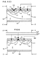
- Figs. 5a-5c there are shown alternative tunnel injectors formed by altering the relative position and size of the N ++ contact region and the P ++ source region.
- These are alternative structures to the structure shown in Fig. 3 between lines AA' and BB'.
- the length of the source region X 2 should be less than the length X 1 of the contact region in order to minimize the size of the source region and thus the size of the emitter of the parasitic transistor which minimizes the injection efficiency of holes from the source region into the N well region.
- Any one of these structures shown with an FET having a contact structure in accordance with the teachings of this invention can be used either as part of a CMOS arrangement or separately.
- FIG. 6 there is shown another alternative structure to that shown in Fig. 3 between lines CC' and DD'.
- This shows the N-channel transistor of the CMOS shown in Fig. 3 with a contact structure in accordance with the teachings of this invention at its source region 56.
- Region 56 is a N ++ degeneratively doped region and region 64 is a P ++ degeneratively doped region. if this structure is used in the device of Fig. 3 then contact region 62 must be connected to ground.
Claims (8)
Applications Claiming Priority (2)
| Application Number | Priority Date | Filing Date | Title |
|---|---|---|---|
| US48102383A | 1983-03-31 | 1983-03-31 | |
| US481023 | 1983-03-31 |
Publications (3)
| Publication Number | Publication Date |
|---|---|
| EP0121096A2 EP0121096A2 (fr) | 1984-10-10 |
| EP0121096A3 EP0121096A3 (en) | 1986-02-12 |
| EP0121096B1 true EP0121096B1 (fr) | 1989-01-04 |
Family
ID=23910272
Family Applications (1)
| Application Number | Title | Priority Date | Filing Date |
|---|---|---|---|
| EP84102100A Expired EP0121096B1 (fr) | 1983-03-31 | 1984-02-29 | Structure de contact pour semi-conducteur |
Country Status (3)
| Country | Link |
|---|---|
| EP (1) | EP0121096B1 (fr) |
| JP (1) | JPS59184560A (fr) |
| DE (1) | DE3475996D1 (fr) |
Families Citing this family (3)
| Publication number | Priority date | Publication date | Assignee | Title |
|---|---|---|---|---|
| WO1985005224A1 (fr) * | 1984-05-02 | 1985-11-21 | Bell Telephone Manufacturing Company Naamloze Venn | Dispositif et agencement semi-conducteurs |
| US5543642A (en) * | 1991-10-23 | 1996-08-06 | Robert Bosch Gmbh | P-channel transistor |
| DE4134879A1 (de) * | 1991-10-23 | 1993-04-29 | Bosch Gmbh Robert | P-kanal-transistor |
Family Cites Families (4)
| Publication number | Priority date | Publication date | Assignee | Title |
|---|---|---|---|---|
| SE392783B (sv) * | 1975-06-19 | 1977-04-18 | Asea Ab | Halvledaranordning innefattande en tyristor och en felteffekttransistordel |
| JPS5939904B2 (ja) * | 1978-09-28 | 1984-09-27 | 株式会社東芝 | 半導体装置 |
| JPS5654071A (en) * | 1979-10-09 | 1981-05-13 | Nec Corp | Insulated gate field-effect transistor |
| JPS5771169A (en) * | 1980-10-21 | 1982-05-01 | Nec Corp | Semiconductor integrated circuit device |
-
1984
- 1984-01-05 JP JP59000129A patent/JPS59184560A/ja active Pending
- 1984-02-29 EP EP84102100A patent/EP0121096B1/fr not_active Expired
- 1984-02-29 DE DE8484102100T patent/DE3475996D1/de not_active Expired
Also Published As
| Publication number | Publication date |
|---|---|
| EP0121096A2 (fr) | 1984-10-10 |
| JPS59184560A (ja) | 1984-10-19 |
| DE3475996D1 (en) | 1989-02-09 |
| EP0121096A3 (en) | 1986-02-12 |
Similar Documents
| Publication | Publication Date | Title |
|---|---|---|
| US4300152A (en) | Complementary field-effect transistor integrated circuit device | |
| US6413806B1 (en) | Semiconductor device and method for protecting such device from a reversed drain voltage | |
| US4327368A (en) | CMOS Transistor pair with reverse biased substrate to prevent latch-up | |
| US5465189A (en) | Low voltage triggering semiconductor controlled rectifiers | |
| US3470390A (en) | Integrated back-to-back diodes to prevent breakdown of mis gate dielectric | |
| US7518209B2 (en) | Isolation of a high-voltage diode between a high-voltage region and a low-voltage region of an integrated circuit | |
| KR890004472B1 (ko) | Cmos 집적회호 | |
| US4622573A (en) | CMOS contacting structure having degeneratively doped regions for the prevention of latch-up | |
| JPH0240221B2 (fr) | ||
| US6365940B1 (en) | High voltage trigger remote-cathode SCR | |
| US4656491A (en) | Protection circuit utilizing distributed transistors and resistors | |
| US6111289A (en) | Semiconductor device | |
| US5045716A (en) | Integrated circuit in complementary circuit technology comprising a substrate bias voltage generator | |
| US5162888A (en) | High DC breakdown voltage field effect transistor and integrated circuit | |
| US5061981A (en) | Double diffused CMOS with Schottky to drain contacts | |
| US6355513B1 (en) | Asymmetric depletion region for normally off JFET | |
| CA1275457C (fr) | Circuits integres en technologie a circuits complementaires comportant un generateur de polarisation du substrat | |
| US5298769A (en) | GTO thyristor capable of preventing parasitic thyristors from being generated | |
| US4320409A (en) | Complementary field-effect transistor integrated circuit device | |
| Sugino et al. | CMOS latch-up elimination using Schottky barrier PMOS | |
| EP0121096B1 (fr) | Structure de contact pour semi-conducteur | |
| US5414292A (en) | Junction-isolated floating diode | |
| CA1289267C (fr) | Structure de protection contre les effets de verrouillage et les decharges electrostatiques | |
| IE50350B1 (en) | Monolithic integrated cmos circuit | |
| US6084272A (en) | Electrostatic discharge protective circuit for semiconductor device |
Legal Events
| Date | Code | Title | Description |
|---|---|---|---|
| PUAI | Public reference made under article 153(3) epc to a published international application that has entered the european phase |
Free format text: ORIGINAL CODE: 0009012 |
|
| AK | Designated contracting states |
Designated state(s): DE FR GB |
|
| 17P | Request for examination filed |
Effective date: 19841123 |
|
| PUAL | Search report despatched |
Free format text: ORIGINAL CODE: 0009013 |
|
| AK | Designated contracting states |
Designated state(s): DE FR GB |
|
| 17Q | First examination report despatched |
Effective date: 19870722 |
|
| GRAA | (expected) grant |
Free format text: ORIGINAL CODE: 0009210 |
|
| AK | Designated contracting states |
Kind code of ref document: B1 Designated state(s): DE FR GB |
|
| REF | Corresponds to: |
Ref document number: 3475996 Country of ref document: DE Date of ref document: 19890209 |
|
| ET | Fr: translation filed | ||
| PLBE | No opposition filed within time limit |
Free format text: ORIGINAL CODE: 0009261 |
|
| STAA | Information on the status of an ep patent application or granted ep patent |
Free format text: STATUS: NO OPPOSITION FILED WITHIN TIME LIMIT |
|
| 26N | No opposition filed | ||
| PGFP | Annual fee paid to national office [announced via postgrant information from national office to epo] |
Ref country code: GB Payment date: 19930118 Year of fee payment: 10 |
|
| PGFP | Annual fee paid to national office [announced via postgrant information from national office to epo] |
Ref country code: FR Payment date: 19930120 Year of fee payment: 10 |
|
| PGFP | Annual fee paid to national office [announced via postgrant information from national office to epo] |
Ref country code: DE Payment date: 19930127 Year of fee payment: 10 |
|
| PG25 | Lapsed in a contracting state [announced via postgrant information from national office to epo] |
Ref country code: GB Effective date: 19940228 |
|
| GBPC | Gb: european patent ceased through non-payment of renewal fee |
Effective date: 19940228 |
|
| PG25 | Lapsed in a contracting state [announced via postgrant information from national office to epo] |
Ref country code: FR Effective date: 19941031 |
|
| PG25 | Lapsed in a contracting state [announced via postgrant information from national office to epo] |
Ref country code: DE Effective date: 19941101 |
|
| REG | Reference to a national code |
Ref country code: FR Ref legal event code: ST |