-
The present invention relates generally to multiplexed analog-to-digital converters particularly but not exclusively useful in television receivers having digital signal processing.
-
Digital signal processing is being applied to television (TV) receivers wherein the video signals are converted from analog signals to digital samples by an analog-to-digital converter (ADC). It is desirable Lo also apply digital signal processing to the sound portions of the TV signal.
-
For the NTSC system used in The United States, the video bandwidth is about 4.2 Megahertz (MHz) so that the minimum sampling rate required is 8.4 MHz according to the Nyquist sampling criteria. This rate provides about 534 samples per horizontal TV line. It is convenient to establish the sampling signal at a multiple of the color subcarrier signal frequency fsc which is about 3.58 MHz in the NTSC system. In particular, four times that frequency (i.e., 4f sc = 14.32 MHz) is most convenient in that it both satisfies the Nyquist sampling criteria and facilitates demodulation of quadrature components of the chrominance signals. This sampling rate provides about 910 samples per horizontal TV line, i.e., about 376 more than the minimum number necessary to represent the video signals.
-
It is herein recognized that because ADCs which can operate at the 4fsc sampling rate are expensive and consume significant amounts of power, it is advantageous that the 376 unneeded samples, or at least a portion thereof, be used other than to supply redundant video information.
-
In accordance with the principles of the present invention, an analog-to-digital converter is multiplexed. Apparatus employing the invention comprises sources of analog video and sound signals an analog-to-digital converter and digital video and sound signal processors are provided. The analog video signals include successive horizontal line intervals. Coupling means couple the analog-to-digital converter between the analog video signal source and the digital video signal processor during a first predetermined portion of the horizontal line interval and between the analog sound signal source and the digital sound signal processor during a second predetermined portion of the horizontal line interval which is different from the first predetermined portion.
-
In the drawings:
- FIGURE 1 is a block diagram of a portion of a TV receiver including an embodiment of the present invention;
- FIGURE 2 is a schematic diagram of particular apparatus useful with the embodiment of FIGURE 1;
- . FIGURE 3 is a block diagram of a modification useful in the apparatus of FIGURE 1;
- FIGURES 4 and 7 illustrate waveforms useful in understanding the operation of the apparatus of FIGURE 3 and 5-6, respectively;
- FIGURES 5 and 6 are schematic diagrams of particular apparatus useful with the apparatus of FIGURE 3; and
- FIGURE 8 is a modification useful with the apparatus of FIGURES 1 and 3.
-
In the drawings, single line arrows represent analog signal or single-bit digital signal connections whereas broad arrows represent plural-bit parallel-format digital signal connections. Unless otherwise stated, digital samples are eight-bit parallel signals. Also, in the remainder of the description, clock signals will be designated by upper-case letters (e.g. 4Fsc); the frequency of such clock signals will be designated by lower-case letters (e.g. 4fsc).
-
In the TV receiver of FIGURE 1, television signals from a tuning system (not shown) are applied to first detector 10 which produces therefrom an intermediate frequency (IF) video signal VS and an IF sound signal SS. The video signal VS comprises a picture carrier amplitude modulated by a composite video signal. The composite video signal comprises a luminance component, a .chrominance component modulating a color subcarrier, a color reference burst component, and a synchronizing component. The sound signal SS comprises a sound carrier frequency modulated by an audio signal. In the NTSC standard, for example, the IF picture carrier will have a frequency of about 45.75 MHz, and the IF sound carrier will have a frequency of about 41.25 MHz. Video signals VS .and sound signals SS are separated from the composite IF signal produced by the tuning system by two respective filters in first detector 10.
-
Video signal VS is amplified and bandpass filtered by IF amplifier 12 which can include automatic gain control (AGC) to adjust the amplitude of its output signal to a predetermined level. The output signal from the IF amplifier 12 is applied to a video detector 14. Video detector 14, which may simply comprise a peak detector, demodulates the IF picture carrier signal to produce an analog baseband composite video signal. The baseband video signal is then band limited to about 4.2 MHz by filter 16 to'produce composite video signal CV. This band limiting filtering precludes the generation of aliased signals by the subsequent analog-to-digital conversion process.
-
The composite video signal CV is applied to clock generator 18 and multiplexer (MUX) 20. The clock generator 18 includes a gated phase locked loop which generates the sampling clock signal 4F . The sampling clock signal 4F sc has a frequency four times the frequency, fsc, of the color subcarrier signal and is phase locked to the color reference burst signal component of the composite video signal CV. Clock generator 18 also includes other conventional circuitry for developing other synchronizing signals (not shown).
-
Sound signal SS from the first detector 10 is, for example, heterodyned in mixer 22 with the signal provided by sound local oscillator (L.O.) 24 to translate the frequency of the sound carrier signal to a lower frequency. For example, when the frequency of the sound local oscillator 24 is 41.1 MHz, the 41.25 MHz sound IF carrier is translated to 0.15 MHz. The translated sound signal is applied to bandpass filter 26 which limits the bandwidth of the analog sound signals to about ±110 Kilohertz (KHz) with respect to the 150 KHz (0.15 MHz) sound carrier. The filtered sound signal is then applied to limiter 28. Because the sound signal is frequency modulated, its amplitude is limited by limiter 28. Filter 30 then removes unwanted signals generated by the limiting process and also limits the upper frequency of the sound signal to 260 KHz to preclude the generation of aliased signals by the subsequent analog-to-digital conversion process. Alternatively, sound signal SS could be shifted in frequency and demodulated by a conventional intercarrier sound arrangement.
-
Multiplexer (MUX) 20 receives analog baseband composite video signals CV from filter 16 and analog sound signals from filter 30. MUX 20 applies one of those analog signals to eight-bit analog-to-digital converter (ADC) 34 in accordance with a selection control signal supplied via line 42 from MUX control 40, which is described in detail below. ' ADC 34 produces eight-bit digital words (samples) at the sampling clock rate 4f sc having values corresponding to the levels of analog signals supplied from MUX 20.
-
Demultiplexer (DEMUX) 36 couples digital samples from ADC 34 to one of digital video signal processor 50 and digital sound signal processor 54 in accordance with the selection control signal supplied via line 42 from MUX control 40. Thus, MUX 20 and DEMUX 36 cooperate to couple ADC 34 into a selected one of the video signal path or the sound signal path at given times. In this manner, analog video signals CV are coupled at selected times via ADC 34 to digital video processor 50 which develops the picture signals necessary to develop a picture display on kinescope (KS) 52. In similar manner,. analog sound signals are coupled at other selected times via ADC 34 to digital sound processor 54 which develops the audio signals necessary to produce the sound program on loudspeaker 56.
-
At least thirty-three samples per horizontal TV line are required to satisfy the Nyquist sampling criteria for an analog sound signal which is band limited to 260 KHz as described above. Thus, MU X 20 and DEMUX 36 must couple ADC 34 into the sound signal path for at least thirty-three sound samples, i.e., thirty-three cycles of sampling clock signal 4Fsc, during each horizontal TV line.
-
The arrangement of FIGURE 2 is one embodiment of MUX control 40 of FIGURE 1. This arrangement causes the sound samples to be inserted periodically into the stream of analog samples applied to ADC 34 in place of video samples, i.e., at evenly spaced times essentially contemporaneously with their occurrences. MUX control 40 develops the control signal on line 42 to periodically insert one sound sample into the stream of conversions done by ADC 34. Counter 44 divides the sampling clock signal 4Fsc by an integer number N which is in a range between three and twenty-seven (i.e., 3 S N ≦ 27). The range of acceptable values of N is selected such that at least thirty-three sound samples and at least 534 video samples are provided during each horizontal TV line, thereby satisfying the Nyquist sampling requirement for both the video and sound signals.
-
With N=26, for example, counter 44 produces on . every twenty-sixth cycle of sampling clock 4Fsc a sound signal selection signal on line 42 which controls MUX 20 and DEMUX 36 to couple ADC 34 to pass the sound signals. On the next subsequent cycle of sampling clock 4F , the selection signal outputs at line 42 return to a video signal selection signal restoring MUX 20, ADC 34 and DEMUX 36 to again pass the video signals. This arrangement provides 35 sound conversion samples per horizontal TV line.
-
It is noted that a latch arrangement responsive to the MUX control signal is included in either DEMUX 36 or video processor 50 to latch the last prior digital video sample during the time when DEMUX 36 is passing digital sound samples from ADC 34 to digital sound processor 54. Further, a second latch arrangement is included in either DEMUX 36 or sound processor 54 to hold the last prior digital sound sample when DEMUX 36 is passing digital video samples from ADC 34 to digital video processor 50
-
The arrangement of FIGURES 1 and 2 is advantageously simple; however, it does cause the loss of a small number of picture samples (i.e. samples occurring during the picture information portion of video signal CV) i.e., those picture samples replaced by sound samples.
-
FIGURE 3 shows a modification to the system of FIGURE 1. The elements of FIGURE 3 which correspond to elements of FIGURE 1 are designated by the same reference numbers. This modification includes an arrangement wherein ADC 34 converts thirty-five sound samples as a group at a rapid rate during a predetermined portion of each horizontal TV line rather than periodically throughout the horizontal line as in the arrangement of FIGURE 1. This is done, for example, during the horizontal blanking (retrace) interval or horizontal synchronization pulse interval of of each T.V. line.
-
The arrangement of FIGURE 3 employs a time-compression and time-expansion technique wherein analog sound samples are stored as they occur, are thereafter rapidly converted into digital samples and stored, and the digital sound samples are then read out of storage at substantially the same rate at which they occurred. In particular, the sound samples are applied to ADC 34 (instead of video samples) during a portion of the horizontal blanking interval (retrace) portion of video signal CV so that no picture information video samples are lost, i.e, no picture samples are replaced by sound samples as is the case in the embodiment of FIGURES 1 and.2.
-
Thirty-five analoq samples of the sound signal filter 30 are stored in analog memory 100' during each horizontal TV line sunstantially aszthey occur. These stored samples are applied through multiplexer 20" to ADC 34 at a much higher rate during the horizontal blanking interval of the next TV line. The digital Samples thus developed are applied through demultiplexer 36 to a digital memory 72 at the higher rate. The stored digital samples are subsequently read out of digital memory 72 and applied to digital sound processor 54 at substantially the rate at which they had originally occurred as corresponding analog sound signal samples during the same.line in which they are produced by ADC 34 (i.e.,,the line after they are stored in analog memory 100). During the remainder of each horizontal
-
interval, MUX 20', ADC 34 and DEMUX 36 apply digital video samples corresponding to analpg video signal CV to digital video processor 50 substantially as described above in relation to FIGURE 1. The above operations are performed in response to timing signals developed by clock generator 18' and gating signals developed by MUX control 40' which will be described in detail below.
-
Of the thirty-five sound signal samples per horizontal TV line, two of these will occur during the horizontal blanking interval. - To avoid loss of sound samples during the horizontal blanking interval, analog memory 100 includes memory blocks 101 and 102 which are, for example, two-stage charge-coupled-device (CCD) analog delay lines. Memory blocks 101 and 102- are used to read and write on alternate lines so that one is supplying stored sound samples (reading out) while the other is being used to store sound samples (writing in) and vice versa Memory block 103 is a thirty-three-stage CCD analog delay line which is read out during the horizontal blanking interval of each TV line and stores analog sound samples during the remainder thereof. A demultiplexer (DEMUX) 98 selectively supplies the analog sound signal from filter 30 to the memory blocks 101, 102 and 103 in response to a control signal supplied on line 42C. Similarly, dual shift register 72 includes two thirty-five stage shift registers 72A and 72B in parallel for alternately accepting the corresponding thirty-five digital samples at a high rate and later supplying those samples at a lower rate.
-
The sequence of operation of memory 100 and shift register 72 of FIGURE 3 will now be set forth for a time period encompassing approximately three horizontal line durations as illustrated by FIGURE 4, emphasizing the processing of the sets of sound signal samples. Clock generator 18' develops clocking signals at two rates: a video sampling clock at the relatively higher rate of 4fsc which is four times the color subcarrier frequency fsc (i.e., 910 samples per line) and a sound sampling clock at the relatively lower rate of 4f /26 (i.e., 35 samples per TV line). The latter is developed in a manner similar to that shown in FIGURE 2. Generator 18' develops memory clocking signals MCl, MC2, MC3, MC4A and MC4B shown in FIGURE 4 by selecting from the 4f and the 4f /26 clock signals at predetermined times in response to gating signals supplied via path 80 from MUX control 40'.
-
During the horizontal blanking interval HB1 of a first line Hl, DEMUX 98 applies the analog sound signals to memory block 101 in response to control signals from MUX control 40' via line 42C. Clock generator 18' applies clock signal MC1 shown in FIGURE 4a to memory block 101. During this interval, MC1 is the 4f /26 sound sampling clock signal so that analog sound samples 1 and 2 are stored in CCD memory 101.
-
Also during the horizontal blanking interval HB1, memories 102 and 103 are sequentially selected by MUX 20' and the data stored therein is read out to ADC 34 and digitally stored in shift register 72 as explained in detail below.
-
In the remainder of the first line HI (i.e., the remaining portion of the horizontal blanking interval and the picture information interval), MUX control 40' via lines 42A and 42B causes analog video samples to pass via MUX 20', ADC 34 and DEMUX 36 to digital video processor 50. In addition, MUX control 40' via line 42C causes DEMUX 98 to apply analog sound signals to CCD memory 103. Clock generator 18' applies clock signal MC3 shown in FIGURE 4c to CCD memory 103. During this interval, MC3 is the 4fsc/26 sound sampling clock so that analog sound .samples 3-35 are stored in CCD memory 103. Clock signals MC1 and MC2 to memories 101 and 102, respectively, contain no clock pulses during this interval and so the samples stored in memories' 101 and 102 are unchanged.
-
In the horizontal blanking interval HB2 of a second line H2 immediately after the first line Hl, DEMUX 98 applies the analog sound signals to CCD memory 102 in response to control signals from MUX control 40' via line 42C. Clock generator 18' applies clock signal MC2, which is the 4f sc/26 sound sampling clock during this interval, to memory 102 so that analog sound samples 36 and 37 are stored therein.
-
In addition, during a first portion I of this interval HB2 of the second given TV line, MUX control 40' via line 42A causes MUX 20' to couple memory 101 to ADC 34. During this first portion I, MC1 includes two cycles of the 4f sc sampling clock so that the samples 1 and 2 stored in memory 101 during the horizontal blanking
-
interval (HB1) of the first TV line Hl are converted to corresponding digital samples and stored in shift register 72A. Clock signal MC3 contains no clock pulses during the first portion of this interval so that the samples stored in memory 103 are unchanged. During the remaining portion II of this interval HB2, MUX control 40' causes MUX 20' to couple memory 103 to ADC 34, and clock generator 18' applies clock signal MC3 including thirty-three clock pulses of the 4fsc sampling clock to memory 103 so that analog sound samples 3-35 stored therein are converted to corresponding digital samples and stored in shift register 72A.
-
Shift register 72 is a dual shift register including two thirty-five stage, eight-bit parallel shift registers 72A and 72B connected in parallel and clocked so that one is accepting (shifting-in) data while the other is supplying (shifting-out data) and vice versa. During the horizontal blanking interval HB2 of the second line, clock MC4A shown in FIGURE 4d applied to shift register 72A includes thirty-five clock pulses of the 4fsc sampling clock signal so that samples 1-35 are- shifted into and stored in shift register 72A.
-
In the remainder of this second line H2, analog video samples CV are again passed by MUX 20', ADC 34 and DEMUX 36 and thirty-three new sound samples 38-70 are stored in memory 103 in the manner described above. In addition, samples 1-33 are supplied from shift register 72A to digital sound processor 54 in response to clock signal MC4A which includes thirty-three clock pulses of the 4fsc/26 sound sampling signal.
-
In the horizontal blanking interval HB3 of the third line H3, two additional cycles of the 4fsc/26 sound sampling signal are included in clock signal MC4A to shift samples 34 and 35 from shift register 72A to processor 54. Clocking signals MC2 and MC3 respectively cause samples 36-37 previously stored in memory 102 and samples 38-70 previously stored in memory 103 to be sequentially passed during portions I and II, respectively, of HB3 via MUX 20', ADC 34 and DEMUX 36. The digital samples 36-70 corresponding thereto are stored in shift register 72B in response to clock signal MC4B shown in FIGURE 4e. Clock signal MC4B includes thirty-five clock pulses of the 4f sc sampling signal during HB3. In addition, new sound samples 71 and 72 of the analog sound signals are acquired and stored in memory 101 in response to clock MC1 in like manner to that described for interval HB1.
-
In the remainder of third line H3, new analog sound samples 73-105 are acquired and stored in memory 103 in the manner described above. In addition, clock MC4B includes thirty-three cycles of the 4f /26 sound sampling signals to cause sound samples 36-68 to be read out of shift register 72B and into sound processor 54 in like manner to that described above for the read out of shift register 72A during line H2.
-
Thus, memories 101 and 103 for one line alternate with memories 102 and 103 for the next line to store periodic analog sound samples substantially as they occur and to read out those samples at the higher 4f sc .rate. Similarly, dual shift registers 72A and 72B alternate to store at the higher 4f sc rate digital samples corresponding to those analog sound samples and to read out those digital samples at substantially the rate at which they occurred, but delayed by the duration H of one horizontal line plus a horizontal blanking interval HB.
-
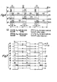
The embodiments of MUX control 40' and clock generator 18' (of FIGURE 3) shown in FIGURES 5 and 6 are suitable for use in the arrangement of FIGURE 3 and will now be described in detail, with reference to the signal waveforms shown in FIGURE 7. MUX control 40' receives horizontal synchronizing pulse HS (FIGURE 7a) and sampling ; clock 4Fsc which are developed in response to the synchronization pulse and color reference burst components of the video signal in conventional fashion. T-type flip-flop 202 toggles in response to positive-going transitions of HS to develop at its output Q a signal (FIGURE 7b) defining alternate TV lines H. AND gates 204 and 206 develop gating signals Gl and G2 (FIGURES 7c and 7d) from signals HS and the complementary outputs from flip-flop 202. Inverter 208 develops gating signal G3 from signal HS. Signals Gl, G2 and G3 are applied to DEMUX 98 of FIGURE 3 via a parallel digital bus 42C.
-
AND gate 210 develops gating signal B (FIGURE 7f) from signals HS and A (FIGURE 7e) the generation of signal A being described below. AND gate 212 develops gating signal G4 (FIGURE 7g) from signals G2 and B, and AND gate 214 develops gating signal G5 (FIGURE 7h) from signals Gl and B. Inverter 216 develops gating signal G6 from signal B. Signals G4, G5 and G6 are applied to MUX 20' of FIGURE 3 via a parallel digital bus 42A.
-
Divide-by-two circuit 220 is reset by the negative-going transition of signal HS to cause inverter 222 to apply a high-logic level to AND gates 210 and 218. Then, the next high-logic level transition of HS enables AND gate 218 to pass sampling signal 4 FSC to develop gated-clocking signal CKl. This enabled condition continues until two clock pulses of the 4 Fsc signal occur on the CKl signal at which time divide-by-two circuit 220 causes inverter 222 to apply a low-logic level to disable AND gate 218. Thus, gated-clocking signal CK1 having the waveform shown in FIGURE 4i is developed.
-
Signal HS is further applied to DEMUX 36 of FIGURE 3 as a gating signal via digital bus 42B. T-type flip-flop 226 toggles in response to positive-going transitions of the signal from inverter 224 which is HS. Flip-flop 226 develops complementary gating signals G7 (FIGURE 7k) and G7 at its respective Q and Q outputs. Signals G7 and G7 represent alternate TV lines H but are delayed by the duration of the high-logic level of signal HS with respect to the signal at the Q output of flip-flop 202. So that flip- flops 202 and 226 are properly synchronized, flip-flop 226 is reset R by the negative-going portion of gating signal G5.
-
Signals GI, G2, G3, G4, G5, G6, G7, G7 and CK1 are applied from MUX control 40' to clock generator 18' via parallel digital bus 80.
-
Clock generator 18' of FIGURE 6 includes a divide-by-twenty-six circuit 300 to develop the 4Fsc/26 sound sampling signal from the 4Fsc sampling signal. AND gate 302 combines gating signal G4 and gated clock signal CK1. AND gate 304 combines gating signal Gl and the 4Fsc/26 sampling signal. OR gate 306 combines the outputs from AND gates 302 and 304 to develop memory clock signal MC1 (FIGURE 4a). In similar manner, AND gates 308 and 310 and OR gate 312 combine gating signals G2 and G5 and signals CK1 and 4F /26 to develop clocking signal MC2 (FIGURE 4b).
-
AND gate 314 combines gating signal G3 and sampling signal 4Fsc/26 to cause OR gate 316 to develop a portion of memory clock signal MC3. Divide-by-thirty-three circuit 320 is reset by the negative-going transition of gating signal G6 to cause inverter 322 to apply a high-logic level to AND gate 318. Then the next high-logic level transition of G6 enables AND gate 318 to pass sampling signal 4Fsc to develop gated-clocking signal CK2. This enabled condition continues until thirty-three clock pulses of the 4F sc signal occur on the CK2 signal at . which time divide-by-thirty-three circuit 320 causes inverter 322 to apply a low-logic level to disable AND gate 318. Thus, gated-clocking signal CK2 having the waveform shown in FIGURE 7j is developed. OR gate 316 combines CK2 with the output from AND gate 314 to develop memory clocking signal MC3 (FIGURE 4d).
-
Sampling signals 4Fsc and 4Fsc/26 are combined with gating signals Gl and G7 by AND gates 324 and 326 respectively and by OR gate 328 to develop shift register clocking signal MC4A (FIGURE 4d). Similarly, sampling signals 4Fsc and 4Fsc/26 are combined with gating signals G2 and G7 by AND gates 328 and 330 respectively and by OR gate 332 to develop shift register clocking signal MC4B (FIGURE 4e).
-
Signals 4FSC and HS are applied from clock generator 181 to MUX control 40' via parallel digital bus 80.
-
Modifications are contemplated to the present invention which is limited only by the claims following. For example, more than the minimum number thirty-three of sound samples can be utilized. If four times that number (i.e., 132 samples) are used, the over-sampling information can be used by digital sound signal processor 54 to calculate an additional bit of resolution. Practically, however, unless a higher frequency sampling clock is employed, the number of sound samples stored is limited to about 143 because the clock signal 4F sc has only about 143 cycles during the approximately ten microsecond duration of the horizontal blanking interval.
-
It is not necessary'that mixer 22 be used to shift the sound IF signal 22 to a lower frequency. FIGURE 8 shows a modification in which mixer 22 is eliminated and sound signal SS at the IF frequency from detector 10 is filtered by bandpass filter 26' and applied via limiter 28 and filter 30 to ADC 34. ADC 34 operates at the 4fsc sampling rate to develop digital samples corresponding to the IF sound signal. The ADC will then directly demodulate the sound signal as described in our GB Patent Application2117988A entitled DIGITAL TELEVISION RECEIVERS. The 4fsc sampling rate satisfies the Nyquist criteria with respect to the bandwidth of the information bearing sidebands about the IF carrier frequency.
-
Analog storage devices other than the CCD delay lines 101, 102 and 103 described herein could be employed; for example, a plurality of capacitive sample-and-hold arrangements or bucket brigade devices are satisfactory.