EP0117128A2 - Multiplexer Analog-Digital-Umwandler - Google Patents
Multiplexer Analog-Digital-Umwandler Download PDFInfo
- Publication number
- EP0117128A2 EP0117128A2 EP84300987A EP84300987A EP0117128A2 EP 0117128 A2 EP0117128 A2 EP 0117128A2 EP 84300987 A EP84300987 A EP 84300987A EP 84300987 A EP84300987 A EP 84300987A EP 0117128 A2 EP0117128 A2 EP 0117128A2
- Authority
- EP
- European Patent Office
- Prior art keywords
- analog
- digital
- samples
- signal
- signals
- Prior art date
- Legal status (The legal status is an assumption and is not a legal conclusion. Google has not performed a legal analysis and makes no representation as to the accuracy of the status listed.)
- Withdrawn
Links
- 230000005236 sound signal Effects 0.000 claims abstract description 67
- 230000008878 coupling Effects 0.000 claims abstract description 15
- 238000010168 coupling process Methods 0.000 claims abstract description 15
- 238000005859 coupling reaction Methods 0.000 claims abstract description 15
- 230000015654 memory Effects 0.000 claims description 51
- 238000005070 sampling Methods 0.000 claims description 42
- 230000004044 response Effects 0.000 claims description 17
- 230000000737 periodic effect Effects 0.000 claims description 6
- 238000006243 chemical reaction Methods 0.000 claims description 5
- 230000003111 delayed effect Effects 0.000 claims description 4
- 239000002131 composite material Substances 0.000 description 8
- 230000004048 modification Effects 0.000 description 6
- 238000012986 modification Methods 0.000 description 6
- 230000007704 transition Effects 0.000 description 6
- 238000010586 diagram Methods 0.000 description 4
- 238000000034 method Methods 0.000 description 4
- 230000009977 dual effect Effects 0.000 description 3
- 230000008569 process Effects 0.000 description 3
- 230000000295 complement effect Effects 0.000 description 2
- 238000007906 compression Methods 0.000 description 1
- 238000001914 filtration Methods 0.000 description 1
- 230000001360 synchronised effect Effects 0.000 description 1
Images


Classifications
-
- H—ELECTRICITY
- H04—ELECTRIC COMMUNICATION TECHNIQUE
- H04N—PICTORIAL COMMUNICATION, e.g. TELEVISION
- H04N9/00—Details of colour television systems
- H04N9/64—Circuits for processing colour signals
Definitions
- the present invention relates generally to multiplexed analog-to-digital converters particularly but not exclusively useful in television receivers having digital signal processing.
- Digital signal processing is being applied to television (TV) receivers wherein the video signals are converted from analog signals to digital samples by an analog-to-digital converter (ADC). It is desirable Lo also apply digital signal processing to the sound portions of the TV signal.
- ADC analog-to-digital converter
- the video bandwidth is about 4.2 Megahertz (MHz) so that the minimum sampling rate required is 8.4 MHz according to the Nyquist sampling criteria.
- This sampling rate provides about 910 samples per horizontal TV line, i.e., about 376 more than the minimum number necessary to represent the video signals.
- an analog-to-digital converter is multiplexed.
- Apparatus employing the invention comprises sources of analog video and sound signals an analog-to-digital converter and digital video and sound signal processors are provided.
- the analog video signals include successive horizontal line intervals.
- Coupling means couple the analog-to-digital converter between the analog video signal source and the digital video signal processor during a first predetermined portion of the horizontal line interval and between the analog sound signal source and the digital sound signal processor during a second predetermined portion of the horizontal line interval which is different from the first predetermined portion.
- single line arrows represent analog signal or single-bit digital signal connections whereas broad arrows represent plural-bit parallel-format digital signal connections.
- digital samples are eight-bit parallel signals.
- clock signals will be designated by upper-case letters (e.g. 4F sc ); the frequency of such clock signals will be designated by lower-case letters (e. g. 4f sc ).
- the video signal VS comprises a picture carrier amplitude modulated by a composite video signal.
- the composite video signal comprises a luminance component, a .chrominance component modulating a color subcarrier, a color reference burst component, and a synchronizing component.
- the sound signal SS comprises a sound carrier frequency modulated by an audio signal.
- the IF picture carrier will have a frequency of about 45.75 MHz, and the IF sound carrier will have a frequency of about 41.25 MHz.
- Video signals VS .and sound signals SS are separated from the composite IF signal produced by the tuning system by two respective filters in first detector 10.
- Video signal VS is amplified and bandpass filtered by IF amplifier 12 which can include automatic gain control (AGC) to adjust the amplitude of its output signal to a predetermined level.
- AGC automatic gain control
- the output signal from the IF amplifier 12 is applied to a video detector 14.
- the baseband video signal is then band limited to about 4.2 MHz by filter 16 to'produce composite video signal CV. This band limiting filtering precludes the generation of aliased signals by the subsequent analog-to-digital conversion process.
- the composite video signal CV is applied to clock generator 18 and multiplexer (MUX) 20.
- the clock generator 18 includes a gated phase locked loop which generates the sampling clock signal 4F .
- the sampling clock signal 4F sc has a frequency four times the frequency, f sc , of the color subcarrier signal and is phase locked to the color reference burst signal component of the composite video signal CV.
- Clock generator 18 also includes other conventional circuitry for developing other synchronizing signals (not shown).
- Sound signal SS from the first detector 10 is, for example, heterodyned in mixer 22 with the signal provided by sound local oscillator (L.O.) 24 to translate the frequency of the sound carrier signal to a lower frequency.
- L.O. sound local oscillator
- the 41.25 MHz sound IF carrier is translated to 0.15 MHz.
- the translated sound signal is applied to bandpass filter 26 which limits the bandwidth of the analog sound signals to about ⁇ 110 Kilohertz (KHz) with respect to the 150 KHz (0.15 MHz) sound carrier.
- KHz Kilohertz
- the filtered sound signal is then applied to limiter 28. Because the sound signal is frequency modulated, its amplitude is limited by limiter 28.
- Filter 30 then removes unwanted signals generated by the limiting process and also limits the upper frequency of the sound signal to 260 KHz to preclude the generation of aliased signals by the subsequent analog-to-digital conversion process.
- sound signal SS could be shifted in frequency and demodulated by a conventional intercarrier sound arrangement.
- Multiplexer (MUX) 20 receives analog baseband composite video signals CV from filter 16 and analog sound signals from filter 30. MUX 20 applies one of those analog signals to eight-bit analog-to-digital converter (ADC) 34 in accordance with a selection control signal supplied via line 42 from MUX control 40, which is described in detail below. ' ADC 34 produces eight-bit digital words (samples) at the sampling clock rate 4f sc having values corresponding to the levels of analog signals supplied from MUX 20.
- ADC analog-to-digital converter
- Demultiplexer (DEMUX) 36 couples digital samples from ADC 34 to one of digital video signal processor 50 and digital sound signal processor 54 in accordance with the selection control signal supplied via line 42 from MUX control 40.
- MUX 20 and DEMUX 36 cooperate to couple ADC 34 into a selected one of the video signal path or the sound signal path at given times.
- analog video signals CV are coupled at selected times via ADC 34 to digital video processor 50 which develops the picture signals necessary to develop a picture display on kinescope (K S ) 52.
- analog sound signals are coupled at other selected times via ADC 34 to digital sound processor 54 which develops the audio signals necessary to produce the sound program on loudspeaker 56.
- At least thirty-three samples per horizontal TV line are required to satisfy the Nyquist sampling criteria for an analog sound signal which is band limited to 260 KHz as described above.
- MU X 20 and DEMUX 36 must couple ADC 34 into the sound signal path for at least thirty-three sound samples, i.e., thirty-three cycles of sampling clock signal 4F sc , during each horizontal T V line.
- FIGURE 2 is one embodiment of MUX control 40 of FIGURE 1.
- This arrangement causes the sound samples to be inserted periodically into the stream of analog samples applied to ADC 34 in place of video samples, i.e., at evenly spaced times essentially contemporaneously with their occurrences.
- MUX control 40 develops the control signal on line 42 to periodically insert one sound sample into the stream of conversions done by ADC 34.
- Counter 44 divides the sampling clock signal 4F sc by an integer number N which is in a range between three and twenty-seven (i.e., 3 S N ⁇ 27).
- the range of acceptable values of N is selected such that at least thirty-three sound samples and at least 534 video samples are provided during each horizontal TV line, thereby satisfying the Nyquist sampling requirement for both the video and sound signals.
- counter 44 produces on . every twenty-sixth cycle of sampling clock 4F sc a sound signal selection signal on line 42 which controls MUX 20 and DEMUX 36 to couple ADC 34 to pass the sound signals.
- the selection signal outputs at line 42 return to a video signal selection signal restoring MUX 20, ADC 34 and DEMUX 36 to again pass the video signals.
- This arrangement provides 35 sound conversion samples per horizontal TV line.
- a latch arrangement responsive to the MUX control signal is included in either DEMUX 36 or video processor 50 to latch the last prior digital video sample during the time when DEMUX 36 is passing digital sound samples from ADC 34 to digital sound processor 54. Further, a second latch arrangement is included in either DEMUX 36 or sound processor 54 to hold the last prior digital sound sample when DEMUX 36 is passing digital video samples from ADC 34 to digital video processor 50
- FIGURES 1 and 2 are advantageously simple; however, it does cause the loss of a small number of picture samples (i.e. samples occurring during the picture information portion of video signal CV) i.e., those picture samples replaced by sound samples.
- FIGURE 3 shows a modification to the system of FIGURE 1.
- the elements of FIGURE 3 which correspond to elements of FIGURE 1 are designated by the same reference numbers.
- This modification includes an arrangement wherein ADC 34 converts thirty-five sound samples as a group at a rapid rate during a predetermined portion of each horizontal TV line rather than periodically throughout the horizontal line as in the arrangement of FIGURE 1. This is done, for example, during the horizontal blanking (retrace) interval or horizontal synchronization pulse interval of of each T.V. line.
- FIGURE 3 employs a time-compression and time-expansion technique wherein analog sound samples are stored as they occur, are thereafter rapidly converted into digital samples and stored, and the digital sound samples are then read out of storage at substantially the same rate at which they occurred.
- the sound samples are applied to ADC 34 (instead of video samples) during a portion of the horizontal blanking interval (retrace) portion of video signal CV so that no picture information video samples are lost, i.e, no picture samples are replaced by sound samples as is the case in the embodiment of FIGURES 1 and.2.
- MUX 20', ADC 34 and DEMUX 36 apply digital video samples corresponding to analpg video signal CV to digital video processor 50 substantially as described above in relation to FIGURE 1.
- the above operations are performed in response to timing signals developed by clock generator 18' and gating signals developed by MUX control 40' which will be described in detail below.
- analog memory 100 includes memory blocks 101 and 102 which are, for example, two-stage charge-coupled-device (CCD) analog delay lines. Memory blocks 101 and 102- are used to read and write on alternate lines so that one is supplying stored sound samples (reading out) while the other is being used to store sound samples (writing in) and vice versa Memory block 103 is a thirty-three-stage CCD analog delay line which is read out during the horizontal blanking interval of each TV line and stores analog sound samples during the remainder thereof.
- CCD charge-coupled-device
- a demultiplexer (DEMUX) 98 selectively supplies the analog sound signal from filter 30 to the memory blocks 101, 102 and 103 in response to a control signal supplied on line 42C.
- dual shift register 72 includes two thirty-five stage shift registers 72A and 72B in parallel for alternately accepting the corresponding thirty-five digital samples at a high rate and later supplying those samples at a lower rate.
- Clock generator 18' develops clocking signals at two rates: a video sampling clock at the relatively higher rate of 4f sc which is four times the color subcarrier frequency f sc (i.e., 910 samples per line) and a sound sampling clock at the relatively lower rate of 4f /26 (i.e., 35 samples per TV line). The latter is developed in a manner similar to that shown in FIGURE 2.
- Generator 18' develops memory clocking signals MCl, MC2, MC3, MC4A and MC4B shown in FIGURE 4 by selecting from the 4f and the 4f /26 clock signals at predetermined times in response to gating signals supplied via path 80 from MUX control 40'.
- DEMUX 98 applies the analog sound signals to memory block 101 in response to control signals from MUX control 40' via line 42C.
- Clock generator 18' applies clock signal MC1 shown in FIGURE 4a to memory block 101.
- MC1 is the 4f /26 sound sampling clock signal so that analog sound samples 1 and 2 are stored in CCD memory 101.
- memories 102 and 103 are sequentially selected by MUX 20' and the data stored therein is read out to ADC 34 and digitally stored in shift register 72 as explained in detail below.
- MUX control 40' via lines 42A and 42B causes analog video samples to pass via MUX 20', ADC 34 and DEMUX 36 to digital video processor 50.
- MUX control 40' via line 42C causes DEMUX 98 to apply analog sound signals to CCD memory 103.
- Clock generator 18' applies clock signal MC3 shown in FIGURE 4c to CCD memory 103. During this interval, M C 3 is the 4f sc /26 sound sampling clock so that analog sound .samples 3-35 are stored in CCD memory 103.
- DEMUX 98 applies the analog sound signals to CCD memory 102 in response to control signals from MUX control 40' via line 42C.
- Clock generator 18' applies clock signal MC2, which is the 4f sc/ 26 sound sampling clock during this interval, to memory 102 so that analog sound samples 36 and 37 are stored therein.
- MUX control 40' via line 42A causes MUX 20' to couple memory 101 to ADC 34.
- MC1 includes two cycles of the 4f sc sampling clock so that the samples 1 and 2 stored in memory 101 during the horizontal blanking
- interval (HB1) of the first TV line Hl are converted to corresponding digital samples and stored in shift register 72A.
- Clock signal MC3 contains no clock pulses during the first portion of this interval so that the samples stored in memory 103 are unchanged.
- MUX control 40' causes MUX 20' to couple memory 103 to ADC 34, and clock generator 18' applies clock signal MC3 including thirty-three clock pulses of the 4f sc sampling clock to memory 103 so that analog sound samples 3-35 stored therein are converted to corresponding digital samples and stored in shift register 72A.
- Shift register 72 is a dual shift register including two thirty-five stage, eight-bit parallel shift registers 72A and 72B connected in parallel and clocked so that one is accepting (shifting-in) data while the other is supplying (shifting-out data) and vice versa.
- clock MC4A shown in FIGURE 4d applied to shift register 72A includes thirty-five clock pulses of the 4f sc sampling clock signal so that samples 1-35 are- shifted into and stored in shift register 72A.
- analog video samples CV are again passed by MUX 20', ADC 34 and DEMUX 36 and thirty-three new sound samples 38-70 are stored in memory 103 in the manner described above.
- samples 1-33 are supplied from shift register 72A to digital sound processor 54 in response to clock signal MC4A which includes thirty-three clock pulses of the 4f sc /26 sound sampling signal.
- Clocking signals MC2 and MC3 respectively cause samples 36-37 previously stored in memory 102 and samples 38-70 previously stored in memory 103 to be sequentially passed during portions I and II, respectively, of HB3 via MUX 20', ADC 34 and DEMUX 36.
- the digital samples 36-70 corresponding thereto are stored in shift register 72B in response to clock signal MC4B shown in FIGURE 4e.
- Clock signal MC4B includes thirty-five clock pulses of the 4f sc sampling signal during HB3.
- new sound samples 71 and 72 of the analog sound signals are acquired and stored in memory 101 in response to clock MC1 in like manner to that described for interval HB1.
- clock MC4B includes thirty-three cycles of the 4f /26 sound sampling signals to cause sound samples 36-68 to be read out of shift register 72B and into sound processor 54 in like manner to that described above for the read out of shift register 72A during line H2.
- memories 101 and 103 for one line alternate with memories 102 and 103 for the next line to store periodic analog sound samples substantially as they occur and to read out those samples at the higher 4f sc .rate.
- dual shift registers 72A and 72B alternate to store at the higher 4f sc rate digital samples corresponding to those analog sound samples and to read out those digital samples at substantially the rate at which they occurred, but delayed by the duration H of one horizontal line plus a horizontal blanking interval HB.
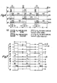
- MUX control 40' and clock generator 18' (of FIGURE 3) shown in FIGURES 5 and 6 are suitable for use in the arrangement of FIGURE 3 and will now be described in detail, with reference to the signal waveforms shown in FIGURE 7.
- MUX control 40' receives horizontal synchronizing pulse HS (FIGURE 7a) and sampling ; clock 4F sc which are developed in response to the synchronization pulse and color reference burst components of the video signal in conventional fashion.
- T-type flip-flop 202 toggles in response to positive-going transitions of HS to develop at its output Q a signal (FIGURE 7b) defining alternate TV lines H.
- AND gates 204 and 206 develop gating signals Gl and G2 (FIGURES 7c and 7d) from signals HS and the complementary outputs from flip-flop 202.
- Inverter 208 develops gating signal G3 from signal HS.
- Signals Gl, G2 and G3 are applied to DEMUX 98 of FIGURE 3 via a parallel digital bus 42C.
- AND gate 210 develops gating signal B (FIGURE 7f) from signals HS and A (FIGURE 7e) the generation of signal A being described below.
- AND gate 212 develops gating signal G4 (FIGURE 7g) from signals G2 and B, and AND gate 214 develops gating signal G5 (FIGURE 7h) from signals Gl and B.
- Inverter 216 develops gating signal G6 from signal B. Signals G4, G5 and G6 are applied to MUX 20' of FIGURE 3 via a parallel digital bus 42A.
- Divide-by-two circuit 220 is reset by the negative-going transition of signal HS to cause inverter 222 to apply a high-logic level to AND gates 210 and 218. Then, the next high-logic level transition of HS enables AND gate 218 to pass sampling signal 4 F SC to develop gated-clocking signal CKl. This enabled condition continues until two clock pulses of the 4 F sc signal occur on the CKl signal at which time divide-by-two circuit 220 causes inverter 222 to apply a low-logic level to disable AND gate 218. Thus, gated-clocking signal CK1 having the waveform shown in FIGURE 4i is developed.
- Signal HS is further applied to DEMUX 36 of FIGURE 3 as a gating signal via digital bus 42B.
- T-type flip-flop 226 toggles in response to positive-going transitions of the signal from inverter 224 which is HS.
- Flip-flop 226 develops complementary gating signals G7 (FIGURE 7k) and G7 at its respective Q and Q outputs.
- Signals G7 and G7 represent alternate TV lines H but are delayed by the duration of the high-logic level of signal HS with respect to the signal at the Q output of flip-flop 202. So that flip-flops 202 and 226 are properly synchronized, flip-flop 226 is reset R by the negative-going portion of gating signal G5.
- Signals GI, G2, G3, G4, G5, G6, G7, G7 and CK1 are applied from MUX control 40' to clock generator 18' via parallel digital bus 80.
- Clock generator 18' of FIGURE 6 includes a divide-by-twenty-six circuit 300 to develop the 4F sc /26 sound sampling signal from the 4F sc sampling signal.
- AND gate 302 combines gating signal G4 and gated clock signal CK1.
- AND gate 304 combines gating signal Gl and the 4F sc /26 sampling signal.
- OR gate 306 combines the outputs from AND gates 302 and 304 to develop memory clock signal MC1 (FIGURE 4a).
- AND gates 308 and 310 and OR gate 312 combine gating signals G2 and G5 and signals CK1 and 4F /26 to develop clocking signal MC2 (FIGURE 4b).
- AND gate 314 combines gating signal G3 and sampling signal 4F sc /26 to cause OR gate 316 to develop a portion of memory clock signal MC3.
- Divide-by-thirty-three circuit 320 is reset by the negative-going transition of gating signal G6 to cause inverter 322 to apply a high-logic level to AND gate 318. Then the next high-logic level transition of G6 enables AND gate 318 to pass sampling signal 4F sc to develop gated-clocking signal CK2. This enabled condition continues until thirty-three clock pulses of the 4F sc signal occur on the CK2 signal at .
- Sampling signals 4F sc and 4F sc /26 are combined with gating signals Gl and G7 by AND gates 324 and 326 respectively and by OR gate 328 to develop shift register clocking signal MC4A (FIGURE 4d).
- sampling signals 4F sc and 4F sc /26 are combined with gating signals G2 and G7 by AND gates 328 and 330 respectively and by OR gate 332 to develop shift register clocking signal MC4B (FIGURE 4e).
- Signals 4F SC and HS are applied from clock generator 18 1 to MUX control 40' via parallel digital bus 80.
- FIGURE 8 shows a modification in which mixer 22 is eliminated and sound signal SS at the IF frequency from detector 10 is filtered by bandpass filter 26' and applied via limiter 28 and filter 30 to ADC 34.
- ADC 34 operates at the 4f sc sampling rate to develop digital samples corresponding to the IF sound signal.
- the ADC will then directly demodulate the sound signal as described in our GB Patent Application2117988A entitled DIGITAL TELEVISION RECEIVERS.
- the 4f sc sampling rate satisfies the Nyquist criteria with respect to the bandwidth of the information bearing sidebands about the IF carrier frequency.
- Analog storage devices other than the CCD delay lines 101, 102 and 103 described herein could be employed; for example, a plurality of capacitive sample-and-hold arrangements or bucket brigade devices are satisfactory.
Landscapes
- Engineering & Computer Science (AREA)
- Multimedia (AREA)
- Signal Processing (AREA)
- Analogue/Digital Conversion (AREA)
- Television Systems (AREA)
- Television Receiver Circuits (AREA)
Applications Claiming Priority (2)
| Application Number | Priority Date | Filing Date | Title |
|---|---|---|---|
| US06/467,284 US4514760A (en) | 1983-02-17 | 1983-02-17 | Digital television receiver with time-multiplexed analog-to-digital converter |
| US467284 | 1983-02-17 |
Publications (2)
| Publication Number | Publication Date |
|---|---|
| EP0117128A2 true EP0117128A2 (de) | 1984-08-29 |
| EP0117128A3 EP0117128A3 (de) | 1985-09-11 |
Family
ID=23855102
Family Applications (1)
| Application Number | Title | Priority Date | Filing Date |
|---|---|---|---|
| EP84300987A Withdrawn EP0117128A3 (de) | 1983-02-17 | 1984-02-15 | Multiplexer Analog-Digital-Umwandler |
Country Status (3)
| Country | Link |
|---|---|
| US (1) | US4514760A (de) |
| EP (1) | EP0117128A3 (de) |
| JP (1) | JPS59161188A (de) |
Cited By (2)
| Publication number | Priority date | Publication date | Assignee | Title |
|---|---|---|---|---|
| GB2157517A (en) * | 1984-04-09 | 1985-10-23 | Yamato Scale Co Ltd | Weighing system |
| EP0245060A2 (de) * | 1986-05-02 | 1987-11-11 | RCA Thomson Licensing Corporation | Frequenzmultiplex-Analog-Digital-Umsetzer |
Families Citing this family (24)
| Publication number | Priority date | Publication date | Assignee | Title |
|---|---|---|---|---|
| US4599640A (en) * | 1984-02-29 | 1986-07-08 | Rca Corporation | Television camera with multiplexed A-D converter |
| US4652903A (en) * | 1984-09-21 | 1987-03-24 | Scientific Atlanta, Inc. | Frequency generation for multiplexed analog component color television encoding and decoding |
| US4652906A (en) * | 1985-03-12 | 1987-03-24 | Racal Data Communications Inc. | Method and apparatus for color decomposition of video signals |
| US4847690A (en) * | 1987-02-19 | 1989-07-11 | Isix, Inc. | Interleaved video system, method and apparatus |
| US4821101A (en) * | 1987-02-19 | 1989-04-11 | Isix, Inc. | Video system, method and apparatus |
| US4994899A (en) * | 1988-03-23 | 1991-02-19 | Scientific Atlanta, Inc. | Frequency generation for extended bandwidth MAC color television encoding and decoding |
| DE3851887T2 (de) * | 1988-07-18 | 1995-04-20 | Ibm | Verfahren und Einrichtung zur Sprachkodierung mit niedriger Bitrate. |
| JP2658236B2 (ja) * | 1988-08-23 | 1997-09-30 | キヤノン株式会社 | 情報処理装置 |
| MY111506A (en) * | 1992-07-29 | 2000-07-31 | Thomson Consumer Electronics Inc | Fir filter apparatus for processing of time division multiplexed signals |
| US5264937A (en) * | 1992-07-29 | 1993-11-23 | Thomson Consumer Electronics, Inc. | Apparatus for time division multiplexed processing of frequency division multiplexed signals |
| US5864592A (en) * | 1992-11-03 | 1999-01-26 | Pairgain Technologies, Inc. | Timing recovery system for digital subscriber line transceivers |
| US5627536A (en) * | 1994-12-27 | 1997-05-06 | Advanced Micro Devices, Inc. | Multiplexed delta-sigma modulator |
| DE19581533C2 (de) * | 1994-12-29 | 1999-02-25 | Motorola Inc | Verfahren zum Digitalisieren eines Breitbandfrequenzsignals und zugehöriger Breitbandfrequenzsignaldigitalisierer |
| US5579341A (en) * | 1994-12-29 | 1996-11-26 | Motorola, Inc. | Multi-channel digital transceiver and method |
| US5754597A (en) * | 1994-12-29 | 1998-05-19 | Motorola, Inc. | Method and apparatus for routing a digitized RF signal to a plurality of paths |
| US5854813A (en) * | 1994-12-29 | 1998-12-29 | Motorola, Inc. | Multiple access up converter/modulator and method |
| US5748683A (en) * | 1994-12-29 | 1998-05-05 | Motorola, Inc. | Multi-channel transceiver having an adaptive antenna array and method |
| US5602874A (en) * | 1994-12-29 | 1997-02-11 | Motorola, Inc. | Method and apparatus for reducing quantization noise |
| US5668836A (en) * | 1994-12-29 | 1997-09-16 | Motorola, Inc. | Split frequency band signal digitizer and method |
| US5710763A (en) * | 1995-07-31 | 1998-01-20 | Motorola, Inc. | Filtered fast Fourier transmultiplexer and method |
| US6094153A (en) * | 1998-02-25 | 2000-07-25 | Intel Corporation | Analog-to-digital converter circuit |
| EP0957635B1 (de) * | 1998-05-15 | 2009-10-07 | Nxp B.V. | Filterschaltung |
| TWI332757B (en) * | 2006-06-14 | 2010-11-01 | Realtek Semiconductor Corp | Circuit and method for reducing mismatch between signal converters |
| US10355709B1 (en) * | 2018-08-24 | 2019-07-16 | Analog Devices, Inc. | Multiplexed sigma-delta analog-to-digital converter |
Citations (1)
| Publication number | Priority date | Publication date | Assignee | Title |
|---|---|---|---|---|
| GB2117988A (en) * | 1982-02-22 | 1983-10-19 | Rca Corp | Digital receivers |
Family Cites Families (16)
| Publication number | Priority date | Publication date | Assignee | Title |
|---|---|---|---|---|
| US3407266A (en) * | 1964-01-29 | 1968-10-22 | Tokyo Shibaura Electric Co | System for reproducing magnetically recorded television signals including a verticalsync pulse generator |
| US3894177A (en) * | 1973-03-23 | 1975-07-08 | Gen Dynamics Corp | Signal distribution system |
| GB1558168A (en) * | 1975-06-20 | 1979-12-19 | Indep Television Co | Systems for broadcasting data simultaneously with but independently of television programmes |
| US4050062A (en) * | 1975-08-14 | 1977-09-20 | The United States Of America As Represented Bythe Secretary Of The Air Force | System for digitizing and interfacing analog data for a digital computer |
| US4027333A (en) * | 1975-12-09 | 1977-05-31 | Cbs Inc. | Multiplex color television transmission system |
| DE2644706C3 (de) * | 1976-10-04 | 1985-12-05 | Robert Bosch Gmbh, 7000 Stuttgart | System zur Übertragung bzw. Speicherung eines Farbfernsehsignals |
| US4159480A (en) * | 1976-10-27 | 1979-06-26 | Sony Corporation | Method of inserting an address signal in a video signal |
| GB1599156A (en) * | 1976-12-24 | 1981-09-30 | Indep Broadcasting Authority | Recording digital signals |
| US4139868A (en) * | 1977-04-21 | 1979-02-13 | The Singer Company | Device for multiplexing video signals |
| FR2389290A1 (fr) * | 1977-04-29 | 1978-11-24 | Briand Marcel | Dispositif d'emission et de reception par lignes analogiques de signaux visiophoniques et de signaux numeriques |
| JPS53142208A (en) * | 1977-05-18 | 1978-12-11 | Teac Corp | Method of recording pcm signal |
| JPS5429610A (en) * | 1977-08-09 | 1979-03-05 | Gen Corp | Method of multiplexing signals |
| US4300161A (en) * | 1980-03-03 | 1981-11-10 | Bell Telephone Laboratories, Incorporated | Time compression multiplexing of video signals |
| US4335393A (en) * | 1980-04-15 | 1982-06-15 | Harris Video Systems, Inc. | Method and system using sequentially encoded color and luminance processing of video type signals to improve picture quality |
| JPS5778288A (en) * | 1980-10-31 | 1982-05-15 | Sony Corp | Recorde |
| US4364080A (en) * | 1981-04-13 | 1982-12-14 | Jovan Vidovic | Digital video analyzer |
-
1983
- 1983-02-17 US US06/467,284 patent/US4514760A/en not_active Expired - Fee Related
-
1984
- 1984-02-15 EP EP84300987A patent/EP0117128A3/de not_active Withdrawn
- 1984-02-16 JP JP59028408A patent/JPS59161188A/ja active Pending
Patent Citations (1)
| Publication number | Priority date | Publication date | Assignee | Title |
|---|---|---|---|---|
| GB2117988A (en) * | 1982-02-22 | 1983-10-19 | Rca Corp | Digital receivers |
Cited By (3)
| Publication number | Priority date | Publication date | Assignee | Title |
|---|---|---|---|---|
| GB2157517A (en) * | 1984-04-09 | 1985-10-23 | Yamato Scale Co Ltd | Weighing system |
| EP0245060A2 (de) * | 1986-05-02 | 1987-11-11 | RCA Thomson Licensing Corporation | Frequenzmultiplex-Analog-Digital-Umsetzer |
| EP0245060A3 (en) * | 1986-05-02 | 1990-10-10 | Rca Corporation | Frequency division multiplexed analog to digital converter |
Also Published As
| Publication number | Publication date |
|---|---|
| EP0117128A3 (de) | 1985-09-11 |
| JPS59161188A (ja) | 1984-09-11 |
| US4514760A (en) | 1985-04-30 |
Similar Documents
| Publication | Publication Date | Title |
|---|---|---|
| US4514760A (en) | Digital television receiver with time-multiplexed analog-to-digital converter | |
| US4646151A (en) | Television frame synchronizer with independently controllable input/output rates | |
| FI80180B (fi) | Kompression av bildelement i en videobild av reducerad storlek. | |
| JP2625102B2 (ja) | Macテレビジョン信号の符号器、復号器、通信方法及びその装置 | |
| US4682251A (en) | Video signal reproducing apparatus having a noise reduction circuit | |
| EP0181189B1 (de) | Verarbeitungssystem für Videosignale | |
| KR910002610B1 (ko) | 디지탈 텔레비젼 신호 처리 시스템 | |
| EP0674437B1 (de) | Videoprozessor mit Halbbildspeicher zur exklusiven Speicherung von Bilddaten | |
| GB2155724A (en) | Multiplexed analog-to-digital converter | |
| US5309224A (en) | Apparatus for converting a television signal of a first television system into a television signal of a second television system employing a digital chrominance signal processing circuit | |
| JPS60134592A (ja) | カラーテレビジヨン送信兼データ記憶システム並びにデータ発生器及び受信機 | |
| JPS592230B2 (ja) | カラ−テレビ信号変換装置 | |
| KR910005254B1 (ko) | 영상기억장치 | |
| JPH0693778B2 (ja) | カラーテレビジヨン信号受信機 | |
| JPS5923149B2 (ja) | 高精細度放送用コンバ−タ | |
| JPS62140580A (ja) | テレビ信号をマルチプレクスするための改良された方法及び装置 | |
| JP2512011B2 (ja) | テレビ信号発生装置 | |
| JPH0360235B2 (de) | ||
| KR930003238Y1 (ko) | 영상신호의 샘플링 장치 | |
| GB2182818A (en) | Burst evaluating circuit | |
| KR0138576B1 (ko) | 화면 크기 변환장치 | |
| JP3108578B2 (ja) | 映像信号処理回路 | |
| JPH01189295A (ja) | 副搬送波の再生方法 | |
| JPS584872B2 (ja) | Secam信号の映像位相調相方式 | |
| JPS62234491A (ja) | 子画面用映像信号生成回路 |
Legal Events
| Date | Code | Title | Description |
|---|---|---|---|
| PUAI | Public reference made under article 153(3) epc to a published international application that has entered the european phase |
Free format text: ORIGINAL CODE: 0009012 |
|
| AK | Designated contracting states |
Designated state(s): DE FR GB |
|
| RAP1 | Party data changed (applicant data changed or rights of an application transferred) |
Owner name: RCA CORPORATION |
|
| PUAL | Search report despatched |
Free format text: ORIGINAL CODE: 0009013 |
|
| AK | Designated contracting states |
Designated state(s): DE FR GB |
|
| 17P | Request for examination filed |
Effective date: 19860211 |
|
| STAA | Information on the status of an ep patent application or granted ep patent |
Free format text: STATUS: THE APPLICATION IS DEEMED TO BE WITHDRAWN |
|
| 18D | Application deemed to be withdrawn |
Effective date: 19870903 |
|
| RIN1 | Information on inventor provided before grant (corrected) |
Inventor name: BALABAN, ALVIN REUBEN Inventor name: STECKLER, STEVEN ALAN |