EP0114531A1 - Package for a semiconductor chip with lead terminals - Google Patents
Package for a semiconductor chip with lead terminals Download PDFInfo
- Publication number
- EP0114531A1 EP0114531A1 EP83307976A EP83307976A EP0114531A1 EP 0114531 A1 EP0114531 A1 EP 0114531A1 EP 83307976 A EP83307976 A EP 83307976A EP 83307976 A EP83307976 A EP 83307976A EP 0114531 A1 EP0114531 A1 EP 0114531A1
- Authority
- EP
- European Patent Office
- Prior art keywords
- lead terminals
- semiconductor chip
- package
- semiconductor device
- outermost
- Prior art date
- Legal status (The legal status is an assumption and is not a legal conclusion. Google has not performed a legal analysis and makes no representation as to the accuracy of the status listed.)
- Granted
Links
Images
Classifications
-
- H—ELECTRICITY
- H01—ELECTRIC ELEMENTS
- H01L—SEMICONDUCTOR DEVICES NOT COVERED BY CLASS H10
- H01L23/00—Details of semiconductor or other solid state devices
- H01L23/48—Arrangements for conducting electric current to or from the solid state body in operation, e.g. leads, terminal arrangements ; Selection of materials therefor
- H01L23/488—Arrangements for conducting electric current to or from the solid state body in operation, e.g. leads, terminal arrangements ; Selection of materials therefor consisting of soldered or bonded constructions
- H01L23/495—Lead-frames or other flat leads
- H01L23/49541—Geometry of the lead-frame
-
- H—ELECTRICITY
- H01—ELECTRIC ELEMENTS
- H01L—SEMICONDUCTOR DEVICES NOT COVERED BY CLASS H10
- H01L24/00—Arrangements for connecting or disconnecting semiconductor or solid-state bodies; Methods or apparatus related thereto
- H01L24/01—Means for bonding being attached to, or being formed on, the surface to be connected, e.g. chip-to-package, die-attach, "first-level" interconnects; Manufacturing methods related thereto
- H01L24/42—Wire connectors; Manufacturing methods related thereto
- H01L24/47—Structure, shape, material or disposition of the wire connectors after the connecting process
- H01L24/49—Structure, shape, material or disposition of the wire connectors after the connecting process of a plurality of wire connectors
-
- H—ELECTRICITY
- H01—ELECTRIC ELEMENTS
- H01L—SEMICONDUCTOR DEVICES NOT COVERED BY CLASS H10
- H01L2224/00—Indexing scheme for arrangements for connecting or disconnecting semiconductor or solid-state bodies and methods related thereto as covered by H01L24/00
- H01L2224/01—Means for bonding being attached to, or being formed on, the surface to be connected, e.g. chip-to-package, die-attach, "first-level" interconnects; Manufacturing methods related thereto
- H01L2224/02—Bonding areas; Manufacturing methods related thereto
- H01L2224/04—Structure, shape, material or disposition of the bonding areas prior to the connecting process
- H01L2224/05—Structure, shape, material or disposition of the bonding areas prior to the connecting process of an individual bonding area
- H01L2224/0554—External layer
- H01L2224/0555—Shape
- H01L2224/05552—Shape in top view
- H01L2224/05554—Shape in top view being square
-
- H—ELECTRICITY
- H01—ELECTRIC ELEMENTS
- H01L—SEMICONDUCTOR DEVICES NOT COVERED BY CLASS H10
- H01L2224/00—Indexing scheme for arrangements for connecting or disconnecting semiconductor or solid-state bodies and methods related thereto as covered by H01L24/00
- H01L2224/01—Means for bonding being attached to, or being formed on, the surface to be connected, e.g. chip-to-package, die-attach, "first-level" interconnects; Manufacturing methods related thereto
- H01L2224/42—Wire connectors; Manufacturing methods related thereto
- H01L2224/47—Structure, shape, material or disposition of the wire connectors after the connecting process
- H01L2224/48—Structure, shape, material or disposition of the wire connectors after the connecting process of an individual wire connector
- H01L2224/4805—Shape
- H01L2224/4809—Loop shape
- H01L2224/48091—Arched
-
- H—ELECTRICITY
- H01—ELECTRIC ELEMENTS
- H01L—SEMICONDUCTOR DEVICES NOT COVERED BY CLASS H10
- H01L2224/00—Indexing scheme for arrangements for connecting or disconnecting semiconductor or solid-state bodies and methods related thereto as covered by H01L24/00
- H01L2224/01—Means for bonding being attached to, or being formed on, the surface to be connected, e.g. chip-to-package, die-attach, "first-level" interconnects; Manufacturing methods related thereto
- H01L2224/42—Wire connectors; Manufacturing methods related thereto
- H01L2224/47—Structure, shape, material or disposition of the wire connectors after the connecting process
- H01L2224/48—Structure, shape, material or disposition of the wire connectors after the connecting process of an individual wire connector
- H01L2224/481—Disposition
- H01L2224/48151—Connecting between a semiconductor or solid-state body and an item not being a semiconductor or solid-state body, e.g. chip-to-substrate, chip-to-passive
- H01L2224/48221—Connecting between a semiconductor or solid-state body and an item not being a semiconductor or solid-state body, e.g. chip-to-substrate, chip-to-passive the body and the item being stacked
- H01L2224/48225—Connecting between a semiconductor or solid-state body and an item not being a semiconductor or solid-state body, e.g. chip-to-substrate, chip-to-passive the body and the item being stacked the item being non-metallic, e.g. insulating substrate with or without metallisation
- H01L2224/48227—Connecting between a semiconductor or solid-state body and an item not being a semiconductor or solid-state body, e.g. chip-to-substrate, chip-to-passive the body and the item being stacked the item being non-metallic, e.g. insulating substrate with or without metallisation connecting the wire to a bond pad of the item
-
- H—ELECTRICITY
- H01—ELECTRIC ELEMENTS
- H01L—SEMICONDUCTOR DEVICES NOT COVERED BY CLASS H10
- H01L2224/00—Indexing scheme for arrangements for connecting or disconnecting semiconductor or solid-state bodies and methods related thereto as covered by H01L24/00
- H01L2224/01—Means for bonding being attached to, or being formed on, the surface to be connected, e.g. chip-to-package, die-attach, "first-level" interconnects; Manufacturing methods related thereto
- H01L2224/42—Wire connectors; Manufacturing methods related thereto
- H01L2224/47—Structure, shape, material or disposition of the wire connectors after the connecting process
- H01L2224/48—Structure, shape, material or disposition of the wire connectors after the connecting process of an individual wire connector
- H01L2224/481—Disposition
- H01L2224/48151—Connecting between a semiconductor or solid-state body and an item not being a semiconductor or solid-state body, e.g. chip-to-substrate, chip-to-passive
- H01L2224/48221—Connecting between a semiconductor or solid-state body and an item not being a semiconductor or solid-state body, e.g. chip-to-substrate, chip-to-passive the body and the item being stacked
- H01L2224/48245—Connecting between a semiconductor or solid-state body and an item not being a semiconductor or solid-state body, e.g. chip-to-substrate, chip-to-passive the body and the item being stacked the item being metallic
- H01L2224/48247—Connecting between a semiconductor or solid-state body and an item not being a semiconductor or solid-state body, e.g. chip-to-substrate, chip-to-passive the body and the item being stacked the item being metallic connecting the wire to a bond pad of the item
-
- H—ELECTRICITY
- H01—ELECTRIC ELEMENTS
- H01L—SEMICONDUCTOR DEVICES NOT COVERED BY CLASS H10
- H01L2224/00—Indexing scheme for arrangements for connecting or disconnecting semiconductor or solid-state bodies and methods related thereto as covered by H01L24/00
- H01L2224/01—Means for bonding being attached to, or being formed on, the surface to be connected, e.g. chip-to-package, die-attach, "first-level" interconnects; Manufacturing methods related thereto
- H01L2224/42—Wire connectors; Manufacturing methods related thereto
- H01L2224/47—Structure, shape, material or disposition of the wire connectors after the connecting process
- H01L2224/49—Structure, shape, material or disposition of the wire connectors after the connecting process of a plurality of wire connectors
- H01L2224/491—Disposition
- H01L2224/4912—Layout
- H01L2224/49171—Fan-out arrangements
-
- H—ELECTRICITY
- H01—ELECTRIC ELEMENTS
- H01L—SEMICONDUCTOR DEVICES NOT COVERED BY CLASS H10
- H01L24/00—Arrangements for connecting or disconnecting semiconductor or solid-state bodies; Methods or apparatus related thereto
- H01L24/01—Means for bonding being attached to, or being formed on, the surface to be connected, e.g. chip-to-package, die-attach, "first-level" interconnects; Manufacturing methods related thereto
- H01L24/42—Wire connectors; Manufacturing methods related thereto
- H01L24/47—Structure, shape, material or disposition of the wire connectors after the connecting process
- H01L24/48—Structure, shape, material or disposition of the wire connectors after the connecting process of an individual wire connector
-
- H—ELECTRICITY
- H01—ELECTRIC ELEMENTS
- H01L—SEMICONDUCTOR DEVICES NOT COVERED BY CLASS H10
- H01L2924/00—Indexing scheme for arrangements or methods for connecting or disconnecting semiconductor or solid-state bodies as covered by H01L24/00
- H01L2924/0001—Technical content checked by a classifier
- H01L2924/00014—Technical content checked by a classifier the subject-matter covered by the group, the symbol of which is combined with the symbol of this group, being disclosed without further technical details
-
- H—ELECTRICITY
- H01—ELECTRIC ELEMENTS
- H01L—SEMICONDUCTOR DEVICES NOT COVERED BY CLASS H10
- H01L2924/00—Indexing scheme for arrangements or methods for connecting or disconnecting semiconductor or solid-state bodies as covered by H01L24/00
- H01L2924/01—Chemical elements
- H01L2924/01015—Phosphorus [P]
-
- H—ELECTRICITY
- H01—ELECTRIC ELEMENTS
- H01L—SEMICONDUCTOR DEVICES NOT COVERED BY CLASS H10
- H01L2924/00—Indexing scheme for arrangements or methods for connecting or disconnecting semiconductor or solid-state bodies as covered by H01L24/00
- H01L2924/01—Chemical elements
- H01L2924/01039—Yttrium [Y]
-
- H—ELECTRICITY
- H01—ELECTRIC ELEMENTS
- H01L—SEMICONDUCTOR DEVICES NOT COVERED BY CLASS H10
- H01L2924/00—Indexing scheme for arrangements or methods for connecting or disconnecting semiconductor or solid-state bodies as covered by H01L24/00
- H01L2924/10—Details of semiconductor or other solid state devices to be connected
- H01L2924/1015—Shape
- H01L2924/1016—Shape being a cuboid
- H01L2924/10161—Shape being a cuboid with a rectangular active surface
-
- H—ELECTRICITY
- H01—ELECTRIC ELEMENTS
- H01L—SEMICONDUCTOR DEVICES NOT COVERED BY CLASS H10
- H01L2924/00—Indexing scheme for arrangements or methods for connecting or disconnecting semiconductor or solid-state bodies as covered by H01L24/00
- H01L2924/10—Details of semiconductor or other solid state devices to be connected
- H01L2924/11—Device type
- H01L2924/14—Integrated circuits
Definitions
- This invention relates to a semiconductor device having a package which has therein a semiconductor chip, such as an integrated circuit (IC) or a large scale integrated circuit (LSI) which is connected to a plurality of lead terminals by means of wires.
- a semiconductor chip such as an integrated circuit (IC) or a large scale integrated circuit (LSI) which is connected to a plurality of lead terminals by means of wires.
- the present invention in particular, relates to an improved arrangement of the connection of the lead terminals and the semiconductor chip.
- the semiconductor chip has bonding pads to which the lead terminals are connected and which are usually located'in the vicinity of the peripheral edges of the chip for the purpose of minimising the length of the wires. If the connecting wires are long , they tend to hang down between the bonding pads and the lead terminals, resulting in so-called wire flow. This wire flow causes the wires to accidentally come into contact with a base of the package which supports the lead terminals, thus resulting in an increased possibility of breakage of the wires, particularly when the semiconductor device is used in a vehicle such as an automobile, which is subject to vibration or impact. Therefore, minimising the length of the connecting wires is very important.
- the base of the package for carrying the semiconductor chip has a peripheral edge adapted to support the terminal ends of the lead terminals (referred to as a margin area hereinafter).
- a margin area In order to make the package itself small and to enable a large semiconductor chip to be received in the package, the width of the margin area must be as small as possible.
- An embodiment of the present invention can provide a semiconductor device in which the lead terminals can be located close to the bonding pads of the semiconductor chip, so that the length of the connecting wires can be decreased, resulting in the device being free from undesirable wire flow.
- a semiconductor device having a package which has therein a semiconductor chip and a plurality of lead terminals which have inner ends received in the package.
- the inner ends of the lead terminals are connected to the semiconductor chip by connecting wires.
- the lead terminals have outer ends which are spaced from one another at a constant pitch.
- the lead terminals located between the outermost lead terminals ( ⁇ xcept perhaps a centre terminal whenpresent)are bent toward the outermost lead terminals, at the intermediate portion of the lead terminals between the outer ends and the inner ends.
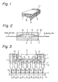
- the semiconductor device has a base 1 which is made of, for example, ceramics.
- the base has a cavity 3 which receives therein a semiconductor chip 5, such as an IC or LSI.
- the semiconductor chip 5 has bonding pads 7 on its peripheral edge.
- the bonding pads 7 are arranged, for example, substantially in two rows along the opposite sides of the peripheral edge thereof.
- Lead terminals 9 are located on the peripheral edge of the base 1.
- the peripheral edge is referred to as a margin area 11.
- lead terminals 9a, 9b, 9c, through 9h are provided on one side of the margin area 11.
- the lead terminals on the opposite side are not shown.
- the lead terminals are connected to the bonding pads 7 by connecting wires 13 in a wire bonding method already known.
- a glass seal ring 15 and a ceramic cap 17 are located on the lead terminals 9 and the base 1, so that they can be all connected together by the glass of the seal ring 15, which is melted by heating.
- the assembly thus obtained forms a semiconductor package (not shown).
- the lead terminals 9 which are parts of a lead frame 21 are cut at the line L in Fig. 3, so that they are independent from each other. Furthermore, the separate lead terminals 9 are usually bent downward at the line L' (Fig. 3) as shown in Fig. 1. The outer ends of the lead terminals 9 are spaced from one another at a constant pitch P, as shown in Fig. 3.
- the pitch P is predetermined in accordance with a standard so as to register with, for example, through-holes of a printed circuit board (not shown) in which the semicondutor device is to be inserted. Hence the pitch P cannot optionally vary.
- the lead terminals 9 are spaced at a constant pitch, corresponding to the pitch P at the outer ends of the lead terminals, from one another even at the inner ends of the lead terminals located in the vicinity of the base 1.
- the pitch between the portions of the lead terminals 9 located at or in the vicinity of the peripheral edge lines of the base 1 is constant. Therefore, the lead terminals between the outermost lead terminals, in particular, the lead terminals 9d and 9e, are located far from the bonding pads 7 on the semiconductor chip 5. That is, the distance between the lead terminal 9d (9e) and the corresponding bonding pad- 7 is S. Therefore, the length of the connecting wires 13, in particular for the lead terminals 9d and 9e, is relatively long, resulting in the the problem of wire flow.
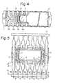
- a small semiconductor chip can be provided in the package, as shown in Fig. 4. This is because, the small semiconductor chip 5 enables the margin area of the base 1 of the package to become large so that the inner ends of the lead terminals which lie on the margin area can be located in the vicinity of and as close as possible to the bonding pads. So, according to the prior art, if a large semiconductor chip is packaged, the connecting wires are inevitably long, and on the other hand, if the connecting wires are required to be short., a small semiconductor chip only can be packaged.
- Fig. 4 shows an actual arrangement of the lead terminals, which is slightly different from that in Fig. 3.
- the portions of the lead terminals that are located in the vicinity of the inner ends thereof are spaced at different pitches, for example as shown in Fig. 5.
- the outer end areas of the lead terminals 9 (9A, 9B, 9C, ..., 9G, 9H) which are designated by X in Fig. 5 are spaced at the predetermined constant pitch P, similar to Fig. 3, since the pitch P can not optionally vary, as mentioned above.
- the inner end areas of the lead terminals that are located in the vicinity of the margin area 11 of the base 1 and that are designated by Y in Fig. 5 have different pitches, i.e., different distances apart.
- the lead terminals which are located between the outermost opposite lead terminals 9A and 9H are bent toward the respective outermost lead terminals.
- all of the intermediate lead terminals between the lead terminals 9A and 9H i.e., the lead terminals 9B, 9C, 9D, 9E, 9F and.9G, are bent toward the respective outermost lead terminals 9A and 9H.
- the lead terminals 9B, 9C, 9D are bent toward the left outermost lead terminals 9A
- the lead terminals 9E, 9F, and 9G are bent toward the right outermost lead terminal 9H.
- only some of the lead terminals between the outerermost lead terminals may be bent, if necessary.
- a center intermediate lead terminal may be straight.
- the inner end areas Y and, accordingly, the inner ends themselves of the lead terminals can be located closer to the bonding pads 7 on the semiconductor chip 5, in comparison with Fig. 3.
- the lengths of the connecting wires-13 can be shortened, thus reducing the possibility of wire flow.
- the connecting wires for the lead terminals 9D and 9E can be remarkably shortened, in comparison with Fig. 3.
- the center intermediate lead terminal 9E may be bent either toward the right or left outermost lead terminal 9A or 9I, in accordance with the location of the relevant bonding pad.
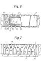
- Figures 6 and 7 also show a large semiconductor chip 5. According to the present invention, as can be easily seen from comparison between Fig. 4 and Fig. 6, a larger semiconductor chip can be packaged.
- Figure 6 shows one example of an actual arrangement of the lead terminals of a product according to the present invention. The packaging of such a larger semiconductor is made possible because the lead terminals between the outermost lead terminals are bent toward the respective outermost lead terminals at the portions of the lead terminals located outside the base 1, as mentioned above, according to the present invention.
- the lengths of the connecting wires can still be shorter than those in the prior art.
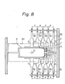
- Figure 8 shows a plastic-molded semiconductor device to which the present invention can also be applied.
- the semiconductor chip 5 is located on the base I' which is a part of the lead frame 21 and which is usually called a die stage. Namely, since there is no base 1 having the cavity 3 as in the ceramic package shown in Figs. 5 to 7, no margin area 11 can be provided on the stage 1'.
- the lead terminals 9 and the semiconductor chip 5 on the stage l' can be molded together by a resin material shown at the imaginary line 30 in Fig. 8. After molding, the portions of the lead frame 21, shown by hatching in Fig. 8, are cut and removed, so that the stage 1', and the lead terminals can be separated from each other.
- the lead terminals are bent toward the respective outermost lead terminals to decrease the lengths of the connecting wires 13, as shown in Fig. 8.
- F ig. 8 shows only half of the arrangement of the lead terminals, since the arrangement is symmetrical with respect to the vertical line as well as the horizontal line crossing the center O (Fig. 8) of the semiconductor chip 5. Namely, arrangements the same as the arrangement of the connections between the lead terminals 9E to 9I and the bonding pads of the semiconductor chip 5 exist also in the left lower quarter. .and left upper quarter, although they are not shown in Fig. 8 for the purpose of clarification.
- the bonding pads can be localized on the peripheral edge of the semiconductor chip, the lengths of the connecting wires for connecting the lead terminals and the bonding pads can be decreased, and a larger semiconductor chip can be packaged in the semiconductor device without making the semiconductor device-itself larger.
Abstract
Description
- This invention relates to a semiconductor device having a package which has therein a semiconductor chip, such as an integrated circuit (IC) or a large scale integrated circuit (LSI) which is connected to a plurality of lead terminals by means of wires. The present invention, in particular, relates to an improved arrangement of the connection of the lead terminals and the semiconductor chip.
- In conventional semiconductor devices, the semiconductor chip has bonding pads to which the lead terminals are connected and which are usually located'in the vicinity of the peripheral edges of the chip for the purpose of minimising the length of the wires. If the connecting wires are long , they tend to hang down between the bonding pads and the lead terminals, resulting in so-called wire flow. This wire flow causes the wires to accidentally come into contact with a base of the package which supports the lead terminals, thus resulting in an increased possibility of breakage of the wires, particularly when the semiconductor device is used in a vehicle such as an automobile, which is subject to vibration or impact. Therefore, minimising the length of the connecting wires is very important.
- On the other hand, larger semiconductor chips are now required, to increase the packaging density thereof, yet smaller packages are required to decrease the size of the semiconductor device (package) as a whole.
- The base of the package for carrying the semiconductor chip has a peripheral edge adapted to support the terminal ends of the lead terminals (referred to as a margin area hereinafter). In order to make the package itself small and to enable a large semiconductor chip to be received in the package, the width of the margin area must be as small as possible.
- Semiconductor devices hithereto known cannot fully satisfy the abovementioned requirements.
- .An embodiment of the present invention can provide a semiconductor device in which the lead terminals can be located close to the bonding pads of the semiconductor chip, so that the length of the connecting wires can be decreased, resulting in the device being free from undesirable wire flow.
- With the decreased length of the connecting wires, it is possible to make the semiconductor device small as a whole and to enable the provision of a large semiconductor chip in the package.
- According to the present invention, there is provided a semiconductor device having a package which has therein a semiconductor chip and a plurality of lead terminals which have inner ends received in the package. The inner ends of the lead terminals are connected to the semiconductor chip by connecting wires. The lead terminals have outer ends which are spaced from one another at a constant pitch. The lead terminals located between the outermost lead terminals (æxcept perhaps a centre terminal whenpresent)are bent toward the outermost lead terminals, at the intermediate portion of the lead terminals between the outer ends and the inner ends.
- The invention will be described below in detail with reference, by way'of example, to the accompanying drawings, in which:
- Figure 1 is a perspective view of a conventional typical semiconductor device:
- Fig. 2 is a sectional view of a conventional semiconductor device according to the prior art;
- Fig. 3 is an enlarged plan view of a part of a conventional semiconductor device shown in Figs. 1 and 2;
- Fig. 4 is a partially sectioned plan view of a semiconductor device according to the prior art;
- Fig. 5 is an enlarged plan view similar to Fig. 3, but according to the present invention;
- Fig. 6 is a partially sectioned plan view similar to Fig. 4, but according to the present invention;
- Fig. 7 is a front elevational view of Fig. 6; and
- Fig. 8 is an enlarged plan view of a part of another embodiment of the present invention.
- Referring first to Figs. 1, 2, and 3, the semiconductor device has a
base 1 which is made of, for example, ceramics. The base has acavity 3 which receives therein asemiconductor chip 5, such as an IC or LSI. Thesemiconductor chip 5 has bondingpads 7 on its peripheral edge. Thebonding pads 7 are arranged, for example, substantially in two rows along the opposite sides of the peripheral edge thereof.Lead terminals 9 are located on the peripheral edge of thebase 1. The peripheral edge is referred to as amargin area 11. - In Fig. 3, eight
lead terminals margin area 11. The lead terminals on the opposite side are not shown. The lead terminals are connected to thebonding pads 7 by connectingwires 13 in a wire bonding method already known. - - In Fig. 2, after the
lead terminals 9 are connected to thecorresponding bonding pads 7 by the connectingwires 13, aglass seal ring 15 and aceramic cap 17 are located on thelead terminals 9 and thebase 1, so that they can be all connected together by the glass of theseal ring 15, which is melted by heating. The assembly thus obtained forms a semiconductor package (not shown). - The
lead terminals 9 which are parts of alead frame 21 are cut at the line L in Fig. 3, so that they are independent from each other. Furthermore, theseparate lead terminals 9 are usually bent downward at the line L' (Fig. 3) as shown in Fig. 1. The outer ends of thelead terminals 9 are spaced from one another at a constant pitch P, as shown in Fig. 3. The pitch P is predetermined in accordance with a standard so as to register with, for example, through-holes of a printed circuit board (not shown) in which the semicondutor device is to be inserted. Hence the pitch P cannot optionally vary. - In the conventional semiconductor device as shown in Figs. 1, 2, and 3, the
lead terminals 9 are spaced at a constant pitch, corresponding to the pitch P at the outer ends of the lead terminals, from one another even at the inner ends of the lead terminals located in the vicinity of thebase 1. In other words, the pitch between the portions of thelead terminals 9 located at or in the vicinity of the peripheral edge lines of thebase 1 is constant. Therefore, the lead terminals between the outermost lead terminals, in particular, thelead terminals bonding pads 7 on thesemiconductor chip 5. That is, the distance between thelead terminal 9d (9e) and the corresponding bonding pad- 7 is S. Therefore, the length of the connectingwires 13, in particular for thelead terminals - Alternatively, if long connecting wires cannot be used because of wire flow, only a small semiconductor chip can be provided in the package, as shown in Fig. 4. This is because, the
small semiconductor chip 5 enables the margin area of thebase 1 of the package to become large so that the inner ends of the lead terminals which lie on the margin area can be located in the vicinity of and as close as possible to the bonding pads. So, according to the prior art, if a large semiconductor chip is packaged, the connecting wires are inevitably long, and on the other hand, if the connecting wires are required to be short., a small semiconductor chip only can be packaged. - It should be noted that Fig. 4 shows an actual arrangement of the lead terminals, which is slightly different from that in Fig. 3.
- According to the present invention, in order to solve the problem, namely, in order to decrease the length of the connecting wires as much as possible, the portions of the lead terminals that are located in the vicinity of the inner ends thereof are spaced at different pitches, for example as shown in Fig. 5.
- As can be seen from Fig. 5, according to the present invention, the outer end areas of the lead terminals 9 (9A, 9B, 9C, ..., 9G, 9H) which are designated by X in Fig. 5 are spaced at the predetermined constant pitch P, similar to Fig. 3, since the pitch P can not optionally vary, as mentioned above. However, the inner end areas of the lead terminals that are located in the vicinity of the
margin area 11 of thebase 1 and that are designated by Y in Fig. 5 have different pitches, i.e., different distances apart. - That is-, according to the present invention, the lead terminals which are located between the outermost
opposite lead terminals lead terminals lead terminals outermost lead terminals lead terminals outermost lead terminals 9A, and thelead terminals outermost lead terminal 9H. However, only some of the lead terminals between the outerermost lead terminals may be bent, if necessary. For example, a center intermediate lead terminal may be straight. - The inner end areas Y and, accordingly, the inner ends themselves of the lead terminals can be located closer to the
bonding pads 7 on thesemiconductor chip 5, in comparison with Fig. 3. As a result of this, the lengths of the connecting wires-13 can be shortened, thus reducing the possibility of wire flow. In particular, the connecting wires for thelead terminals - When the number of the lead terminals is odd,(as shown in Figs. 6 and 7), the center
intermediate lead terminal 9E may be bent either toward the right or leftoutermost lead terminal - Figures 6 and 7 also show a
large semiconductor chip 5. According to the present invention, as can be easily seen from comparison between Fig. 4 and Fig. 6, a larger semiconductor chip can be packaged. Figure 6 shows one example of an actual arrangement of the lead terminals of a product according to the present invention. The packaging of such a larger semiconductor is made possible because the lead terminals between the outermost lead terminals are bent toward the respective outermost lead terminals at the portions of the lead terminals located outside thebase 1, as mentioned above, according to the present invention. - The larger the semiconductor chip, the longer the connecting wires for the intermediate lead terminals, but even if a larger semiconductor chip is packaged, the lengths of the connecting wires can still be shorter than those in the prior art.
- Figure 8 shows a plastic-molded semiconductor device to which the present invention can also be applied. As is well known, in a . plastic-molded semiconductor device, the
semiconductor chip 5 is located on the base I' which is a part of thelead frame 21 and which is usually called a die stage. Namely, since there is nobase 1 having thecavity 3 as in the ceramic package shown in Figs. 5 to 7, nomargin area 11 can be provided on the stage 1'. Thelead terminals 9 and thesemiconductor chip 5 on the stage l' can be molded together by a resin material shown at theimaginary line 30 in Fig. 8. After molding, the portions of thelead frame 21, shown by hatching in Fig. 8, are cut and removed, so that the stage 1', and the lead terminals can be separated from each other. As before, in such a plastic-molded semiconductor package, according to the present invention, the lead terminals are bent toward the respective outermost lead terminals to decrease the lengths of the connectingwires 13, as shown in Fig. 8. - Thus, the same technical idea as the foregoing is applicable also to a plastic-molded semiconductor package as shown in Fig. 8. It should be noted that Fig. 8 shows only half of the arrangement of the lead terminals, since the arrangement is symmetrical with respect to the vertical line as well as the horizontal line crossing the center O (Fig. 8) of the
semiconductor chip 5. Namely, arrangements the same as the arrangement of the connections between thelead terminals 9E to 9I and the bonding pads of thesemiconductor chip 5 exist also in the left lower quarter. .and left upper quarter, although they are not shown in Fig. 8 for the purpose of clarification. - As can be seen from the above mentioned discussion, according to the present invention, the bonding pads can be localized on the peripheral edge of the semiconductor chip, the lengths of the connecting wires for connecting the lead terminals and the bonding pads can be decreased, and a larger semiconductor chip can be packaged in the semiconductor device without making the semiconductor device-itself larger.
Claims (5)
Applications Claiming Priority (2)
| Application Number | Priority Date | Filing Date | Title |
|---|---|---|---|
| JP57231631A JPS59125644A (en) | 1982-12-29 | 1982-12-29 | Semiconductor device |
| JP231631/82 | 1982-12-29 |
Publications (3)
| Publication Number | Publication Date |
|---|---|
| EP0114531A1 true EP0114531A1 (en) | 1984-08-01 |
| EP0114531B1 EP0114531B1 (en) | 1987-03-18 |
| EP0114531B2 EP0114531B2 (en) | 1991-06-26 |
Family
ID=16926529
Family Applications (1)
| Application Number | Title | Priority Date | Filing Date |
|---|---|---|---|
| EP83307976A Expired - Lifetime EP0114531B2 (en) | 1982-12-29 | 1983-12-23 | Package for a semiconductor chip with lead terminals |
Country Status (4)
| Country | Link |
|---|---|
| US (1) | US4575748A (en) |
| EP (1) | EP0114531B2 (en) |
| JP (1) | JPS59125644A (en) |
| DE (1) | DE3370407D1 (en) |
Cited By (7)
| Publication number | Priority date | Publication date | Assignee | Title |
|---|---|---|---|---|
| EP0143441A2 (en) * | 1983-11-26 | 1985-06-05 | Kabushiki Kaisha Toshiba | Lead frame and the method of manufacturing the same |
| EP0242962A1 (en) * | 1986-04-25 | 1987-10-28 | Inmos Corporation | Offset pad semiconductor lead frame |
| GB2254186A (en) * | 1991-03-23 | 1992-09-30 | Samsung Electronics Co Ltd | Semiconductor lead frame |
| GB2323474A (en) * | 1997-03-21 | 1998-09-23 | Rohm Co Ltd | A leadframe for a semiconductor device |
| US6064112A (en) * | 1997-03-25 | 2000-05-16 | Hitachi, Ltd. | Resin-molded semiconductor device having a lead on chip structure |
| GB2368195A (en) * | 1997-03-21 | 2002-04-24 | Rohm Co Ltd | Leadframe diepad |
| DE102007002260A1 (en) | 2007-01-16 | 2008-07-31 | Sanofi-Aventis | Use of substituted pyranonic acid derivatives for the preparation of medicaments for the treatment of the metabolic syndrome |
Families Citing this family (9)
| Publication number | Priority date | Publication date | Assignee | Title |
|---|---|---|---|---|
| JPH0732223B2 (en) * | 1985-01-11 | 1995-04-10 | 三菱電機株式会社 | Semiconductor device |
| US5365113A (en) * | 1987-06-30 | 1994-11-15 | Hitachi, Ltd. | Semiconductor device |
| US5184208A (en) * | 1987-06-30 | 1993-02-02 | Hitachi, Ltd. | Semiconductor device |
| JPH01192154A (en) * | 1988-01-28 | 1989-08-02 | Nippon Motoroola Kk | Lead frame |
| JP2560805B2 (en) * | 1988-10-06 | 1996-12-04 | 三菱電機株式会社 | Semiconductor device |
| JPH0536756A (en) * | 1991-07-30 | 1993-02-12 | Mitsubishi Electric Corp | Tape carrier for semiconductor device and its manufacture |
| JPH05226485A (en) * | 1992-02-12 | 1993-09-03 | Mitsubishi Electric Corp | Semiconductor device |
| US5781682A (en) * | 1996-02-01 | 1998-07-14 | International Business Machines Corporation | Low-cost packaging for parallel optical computer link |
| US9035437B2 (en) | 2013-03-12 | 2015-05-19 | Infineon Technologies Austria Ag | Packaged device comprising non-integer lead pitches and method of manufacturing the same |
Citations (5)
| Publication number | Priority date | Publication date | Assignee | Title |
|---|---|---|---|---|
| FR1532813A (en) * | 1966-07-29 | 1968-07-12 | Texas Instruments Inc | Method of packaging semiconductor devices with multiple connections and product resulting therefrom |
| DE1904118A1 (en) * | 1968-01-29 | 1969-08-28 | Hitachi Ltd | Semiconductor device with improved electrode connection structure |
| CH513521A (en) * | 1969-09-11 | 1971-09-30 | Philips Nv | Method for producing a semiconductor component, wherein a tool is used to make electrical connections between contact points of the semiconductor component on the one hand and supply conductors on the other |
| US3611061A (en) * | 1971-07-07 | 1971-10-05 | Motorola Inc | Multiple lead integrated circuit device and frame member for the fabrication thereof |
| DE7035721U (en) * | 1969-09-29 | 1973-11-15 | Ind Gmbh Deutsche | SELF-ADJUSTING CONTACT FRAME |
Family Cites Families (2)
| Publication number | Priority date | Publication date | Assignee | Title |
|---|---|---|---|---|
| US4066839A (en) * | 1972-11-16 | 1978-01-03 | Sgs-Ates Componenti Elettronici S.P.A. | Molded body incorporating heat dissipator |
| JPS53124649A (en) * | 1977-04-07 | 1978-10-31 | Sanei Kagaku Kogyo Kk | Production of pickles |
-
1982
- 1982-12-29 JP JP57231631A patent/JPS59125644A/en active Pending
-
1983
- 1983-12-23 US US06/564,711 patent/US4575748A/en not_active Expired - Lifetime
- 1983-12-23 DE DE8383307976T patent/DE3370407D1/en not_active Expired
- 1983-12-23 EP EP83307976A patent/EP0114531B2/en not_active Expired - Lifetime
Patent Citations (5)
| Publication number | Priority date | Publication date | Assignee | Title |
|---|---|---|---|---|
| FR1532813A (en) * | 1966-07-29 | 1968-07-12 | Texas Instruments Inc | Method of packaging semiconductor devices with multiple connections and product resulting therefrom |
| DE1904118A1 (en) * | 1968-01-29 | 1969-08-28 | Hitachi Ltd | Semiconductor device with improved electrode connection structure |
| CH513521A (en) * | 1969-09-11 | 1971-09-30 | Philips Nv | Method for producing a semiconductor component, wherein a tool is used to make electrical connections between contact points of the semiconductor component on the one hand and supply conductors on the other |
| DE7035721U (en) * | 1969-09-29 | 1973-11-15 | Ind Gmbh Deutsche | SELF-ADJUSTING CONTACT FRAME |
| US3611061A (en) * | 1971-07-07 | 1971-10-05 | Motorola Inc | Multiple lead integrated circuit device and frame member for the fabrication thereof |
Cited By (12)
| Publication number | Priority date | Publication date | Assignee | Title |
|---|---|---|---|---|
| EP0143441A2 (en) * | 1983-11-26 | 1985-06-05 | Kabushiki Kaisha Toshiba | Lead frame and the method of manufacturing the same |
| EP0143441A3 (en) * | 1983-11-26 | 1986-08-20 | Kabushiki Kaisha Toshiba | Lead frame and the method of manufacturing the same |
| EP0242962A1 (en) * | 1986-04-25 | 1987-10-28 | Inmos Corporation | Offset pad semiconductor lead frame |
| GB2254186A (en) * | 1991-03-23 | 1992-09-30 | Samsung Electronics Co Ltd | Semiconductor lead frame |
| GB2323474A (en) * | 1997-03-21 | 1998-09-23 | Rohm Co Ltd | A leadframe for a semiconductor device |
| US6107676A (en) * | 1997-03-21 | 2000-08-22 | Rohm Co., Ltd. | Leadframe and a method of manufacturing a semiconductor device by use of it |
| GB2368195A (en) * | 1997-03-21 | 2002-04-24 | Rohm Co Ltd | Leadframe diepad |
| GB2323474B (en) * | 1997-03-21 | 2002-07-31 | Rohm Co Ltd | A leadframe and a method of manufacturing a semiconductor device device by use of it |
| GB2368195B (en) * | 1997-03-21 | 2002-07-31 | Rohm Co Ltd | A leadframe and a method of manufacturing a semiconductor device by use of it |
| US6064112A (en) * | 1997-03-25 | 2000-05-16 | Hitachi, Ltd. | Resin-molded semiconductor device having a lead on chip structure |
| DE102007002260A1 (en) | 2007-01-16 | 2008-07-31 | Sanofi-Aventis | Use of substituted pyranonic acid derivatives for the preparation of medicaments for the treatment of the metabolic syndrome |
| US8748483B2 (en) | 2007-01-16 | 2014-06-10 | Sanofi | Use of substituted pyranone acid derivatives for the treatment of metabolic syndrome |
Also Published As
| Publication number | Publication date |
|---|---|
| JPS59125644A (en) | 1984-07-20 |
| EP0114531B2 (en) | 1991-06-26 |
| EP0114531B1 (en) | 1987-03-18 |
| US4575748A (en) | 1986-03-11 |
| DE3370407D1 (en) | 1987-04-23 |
Similar Documents
| Publication | Publication Date | Title |
|---|---|---|
| EP0114531B1 (en) | Package for a semiconductor chip with lead terminals | |
| US6118174A (en) | Bottom lead frame and bottom lead semiconductor package using the same | |
| US5250841A (en) | Semiconductor device with test-only leads | |
| US5413970A (en) | Process for manufacturing a semiconductor package having two rows of interdigitated leads | |
| US5363279A (en) | Semiconductor package for a semiconductor chip having centrally located bottom bond pads | |
| US5783861A (en) | Semiconductor package and lead frame | |
| US4677526A (en) | Plastic pin grid array chip carrier | |
| US6444905B1 (en) | Semiconductor device | |
| US5561086A (en) | Techniques for mounting semiconductor dies in die-receiving areas having support structure having notches | |
| JPH1012658A (en) | Semiconductor integrated circuit element having many input/output terminals | |
| JP2806328B2 (en) | Resin-sealed semiconductor device and method of manufacturing the same | |
| KR100379089B1 (en) | leadframe and semiconductor package using it | |
| KR930004255B1 (en) | Resin sealed semiconductor device | |
| EP0443044A1 (en) | Lead frame for semiconductor device and semiconductor device using the lead frame | |
| KR100566781B1 (en) | Lead on chip type semiconductor package | |
| JP2990645B2 (en) | Lead frame for semiconductor integrated circuit and semiconductor integrated circuit | |
| KR102026314B1 (en) | Semiconductor packet for small production | |
| KR19990034731A (en) | Lead-on chip lead frames and packages using them | |
| US20010050420A1 (en) | Leadframe having joined internal lead | |
| KR980012384A (en) | Lead frame with different inner lead edge | |
| KR100537893B1 (en) | Leadframe and multichip package using the same | |
| EP0242962A1 (en) | Offset pad semiconductor lead frame | |
| KR960004872Y1 (en) | Lead frame structure of plastic quad flat package | |
| KR0142978B1 (en) | Vertical Surface Mount Package Device | |
| JPH03232264A (en) | Lead frame and semiconductor integrated circuit device using same |
Legal Events
| Date | Code | Title | Description |
|---|---|---|---|
| PUAI | Public reference made under article 153(3) epc to a published international application that has entered the european phase |
Free format text: ORIGINAL CODE: 0009012 |
|
| AK | Designated contracting states |
Designated state(s): DE FR GB |
|
| 17P | Request for examination filed |
Effective date: 19840730 |
|
| GRAA | (expected) grant |
Free format text: ORIGINAL CODE: 0009210 |
|
| AK | Designated contracting states |
Kind code of ref document: B1 Designated state(s): DE FR GB |
|
| REF | Corresponds to: |
Ref document number: 3370407 Country of ref document: DE Date of ref document: 19870423 |
|
| ET | Fr: translation filed | ||
| PLBI | Opposition filed |
Free format text: ORIGINAL CODE: 0009260 |
|
| 26 | Opposition filed |
Opponent name: TELEFUNKEN ELECTRONIC GMBH Effective date: 19871216 Opponent name: DEUTSCHE ITT INDUSTRIES GMBH, FREIBURG Effective date: 19871215 |
|
| PUAH | Patent maintained in amended form |
Free format text: ORIGINAL CODE: 0009272 |
|
| STAA | Information on the status of an ep patent application or granted ep patent |
Free format text: STATUS: PATENT MAINTAINED AS AMENDED |
|
| 27A | Patent maintained in amended form |
Effective date: 19910626 |
|
| AK | Designated contracting states |
Kind code of ref document: B2 Designated state(s): DE FR GB |
|
| ET3 | Fr: translation filed ** decision concerning opposition | ||
| PGFP | Annual fee paid to national office [announced via postgrant information from national office to epo] |
Ref country code: GB Payment date: 19921013 Year of fee payment: 10 |
|
| PGFP | Annual fee paid to national office [announced via postgrant information from national office to epo] |
Ref country code: FR Payment date: 19921221 Year of fee payment: 10 |
|
| PGFP | Annual fee paid to national office [announced via postgrant information from national office to epo] |
Ref country code: DE Payment date: 19930226 Year of fee payment: 10 |
|
| PG25 | Lapsed in a contracting state [announced via postgrant information from national office to epo] |
Ref country code: GB Effective date: 19931223 |
|
| GBPC | Gb: european patent ceased through non-payment of renewal fee |
Effective date: 19931223 |
|
| PG25 | Lapsed in a contracting state [announced via postgrant information from national office to epo] |
Ref country code: FR Effective date: 19940831 |
|
| PG25 | Lapsed in a contracting state [announced via postgrant information from national office to epo] |
Ref country code: DE Effective date: 19940901 |
|
| REG | Reference to a national code |
Ref country code: FR Ref legal event code: ST |