EP0113282B1 - Boîtier pour composant électronique comportant un élément fixant l'humidité - Google Patents
Boîtier pour composant électronique comportant un élément fixant l'humidité Download PDFInfo
- Publication number
- EP0113282B1 EP0113282B1 EP83402489A EP83402489A EP0113282B1 EP 0113282 B1 EP0113282 B1 EP 0113282B1 EP 83402489 A EP83402489 A EP 83402489A EP 83402489 A EP83402489 A EP 83402489A EP 0113282 B1 EP0113282 B1 EP 0113282B1
- Authority
- EP
- European Patent Office
- Prior art keywords
- housing
- fixation element
- base
- housing according
- component
- Prior art date
- Legal status (The legal status is an assumption and is not a legal conclusion. Google has not performed a legal analysis and makes no representation as to the accuracy of the status listed.)
- Expired
Links
Images

Classifications
-
- G—PHYSICS
- G01—MEASURING; TESTING
- G01P—MEASURING LINEAR OR ANGULAR SPEED, ACCELERATION, DECELERATION, OR SHOCK; INDICATING PRESENCE, ABSENCE, OR DIRECTION, OF MOVEMENT
- G01P1/00—Details of instruments
- G01P1/02—Housings
- G01P1/023—Housings for acceleration measuring devices
-
- H—ELECTRICITY
- H01—ELECTRIC ELEMENTS
- H01L—SEMICONDUCTOR DEVICES NOT COVERED BY CLASS H10
- H01L23/00—Details of semiconductor or other solid state devices
- H01L23/02—Containers; Seals
- H01L23/04—Containers; Seals characterised by the shape of the container or parts, e.g. caps, walls
- H01L23/053—Containers; Seals characterised by the shape of the container or parts, e.g. caps, walls the container being a hollow construction and having an insulating or insulated base as a mounting for the semiconductor body
- H01L23/057—Containers; Seals characterised by the shape of the container or parts, e.g. caps, walls the container being a hollow construction and having an insulating or insulated base as a mounting for the semiconductor body the leads being parallel to the base
-
- H—ELECTRICITY
- H01—ELECTRIC ELEMENTS
- H01L—SEMICONDUCTOR DEVICES NOT COVERED BY CLASS H10
- H01L23/00—Details of semiconductor or other solid state devices
- H01L23/16—Fillings or auxiliary members in containers or encapsulations, e.g. centering rings
- H01L23/18—Fillings characterised by the material, its physical or chemical properties, or its arrangement within the complete device
- H01L23/26—Fillings characterised by the material, its physical or chemical properties, or its arrangement within the complete device including materials for absorbing or reacting with moisture or other undesired substances, e.g. getters
-
- H—ELECTRICITY
- H01—ELECTRIC ELEMENTS
- H01L—SEMICONDUCTOR DEVICES NOT COVERED BY CLASS H10
- H01L2224/00—Indexing scheme for arrangements for connecting or disconnecting semiconductor or solid-state bodies and methods related thereto as covered by H01L24/00
- H01L2224/01—Means for bonding being attached to, or being formed on, the surface to be connected, e.g. chip-to-package, die-attach, "first-level" interconnects; Manufacturing methods related thereto
- H01L2224/02—Bonding areas; Manufacturing methods related thereto
- H01L2224/04—Structure, shape, material or disposition of the bonding areas prior to the connecting process
- H01L2224/05—Structure, shape, material or disposition of the bonding areas prior to the connecting process of an individual bonding area
- H01L2224/0554—External layer
- H01L2224/0555—Shape
- H01L2224/05552—Shape in top view
- H01L2224/05554—Shape in top view being square
-
- H—ELECTRICITY
- H01—ELECTRIC ELEMENTS
- H01L—SEMICONDUCTOR DEVICES NOT COVERED BY CLASS H10
- H01L2224/00—Indexing scheme for arrangements for connecting or disconnecting semiconductor or solid-state bodies and methods related thereto as covered by H01L24/00
- H01L2224/01—Means for bonding being attached to, or being formed on, the surface to be connected, e.g. chip-to-package, die-attach, "first-level" interconnects; Manufacturing methods related thereto
- H01L2224/42—Wire connectors; Manufacturing methods related thereto
- H01L2224/47—Structure, shape, material or disposition of the wire connectors after the connecting process
- H01L2224/48—Structure, shape, material or disposition of the wire connectors after the connecting process of an individual wire connector
- H01L2224/4805—Shape
- H01L2224/4809—Loop shape
- H01L2224/48091—Arched
-
- H—ELECTRICITY
- H01—ELECTRIC ELEMENTS
- H01L—SEMICONDUCTOR DEVICES NOT COVERED BY CLASS H10
- H01L2224/00—Indexing scheme for arrangements for connecting or disconnecting semiconductor or solid-state bodies and methods related thereto as covered by H01L24/00
- H01L2224/01—Means for bonding being attached to, or being formed on, the surface to be connected, e.g. chip-to-package, die-attach, "first-level" interconnects; Manufacturing methods related thereto
- H01L2224/42—Wire connectors; Manufacturing methods related thereto
- H01L2224/47—Structure, shape, material or disposition of the wire connectors after the connecting process
- H01L2224/48—Structure, shape, material or disposition of the wire connectors after the connecting process of an individual wire connector
- H01L2224/481—Disposition
- H01L2224/48151—Connecting between a semiconductor or solid-state body and an item not being a semiconductor or solid-state body, e.g. chip-to-substrate, chip-to-passive
- H01L2224/48221—Connecting between a semiconductor or solid-state body and an item not being a semiconductor or solid-state body, e.g. chip-to-substrate, chip-to-passive the body and the item being stacked
- H01L2224/48225—Connecting between a semiconductor or solid-state body and an item not being a semiconductor or solid-state body, e.g. chip-to-substrate, chip-to-passive the body and the item being stacked the item being non-metallic, e.g. insulating substrate with or without metallisation
- H01L2224/48227—Connecting between a semiconductor or solid-state body and an item not being a semiconductor or solid-state body, e.g. chip-to-substrate, chip-to-passive the body and the item being stacked the item being non-metallic, e.g. insulating substrate with or without metallisation connecting the wire to a bond pad of the item
-
- H—ELECTRICITY
- H01—ELECTRIC ELEMENTS
- H01L—SEMICONDUCTOR DEVICES NOT COVERED BY CLASS H10
- H01L2224/00—Indexing scheme for arrangements for connecting or disconnecting semiconductor or solid-state bodies and methods related thereto as covered by H01L24/00
- H01L2224/01—Means for bonding being attached to, or being formed on, the surface to be connected, e.g. chip-to-package, die-attach, "first-level" interconnects; Manufacturing methods related thereto
- H01L2224/42—Wire connectors; Manufacturing methods related thereto
- H01L2224/47—Structure, shape, material or disposition of the wire connectors after the connecting process
- H01L2224/48—Structure, shape, material or disposition of the wire connectors after the connecting process of an individual wire connector
- H01L2224/484—Connecting portions
- H01L2224/48463—Connecting portions the connecting portion on the bonding area of the semiconductor or solid-state body being a ball bond
- H01L2224/48465—Connecting portions the connecting portion on the bonding area of the semiconductor or solid-state body being a ball bond the other connecting portion not on the bonding area being a wedge bond, i.e. ball-to-wedge, regular stitch
-
- H—ELECTRICITY
- H01—ELECTRIC ELEMENTS
- H01L—SEMICONDUCTOR DEVICES NOT COVERED BY CLASS H10
- H01L2224/00—Indexing scheme for arrangements for connecting or disconnecting semiconductor or solid-state bodies and methods related thereto as covered by H01L24/00
- H01L2224/01—Means for bonding being attached to, or being formed on, the surface to be connected, e.g. chip-to-package, die-attach, "first-level" interconnects; Manufacturing methods related thereto
- H01L2224/42—Wire connectors; Manufacturing methods related thereto
- H01L2224/47—Structure, shape, material or disposition of the wire connectors after the connecting process
- H01L2224/49—Structure, shape, material or disposition of the wire connectors after the connecting process of a plurality of wire connectors
- H01L2224/491—Disposition
- H01L2224/4912—Layout
- H01L2224/49171—Fan-out arrangements
-
- H—ELECTRICITY
- H01—ELECTRIC ELEMENTS
- H01L—SEMICONDUCTOR DEVICES NOT COVERED BY CLASS H10
- H01L24/00—Arrangements for connecting or disconnecting semiconductor or solid-state bodies; Methods or apparatus related thereto
- H01L24/01—Means for bonding being attached to, or being formed on, the surface to be connected, e.g. chip-to-package, die-attach, "first-level" interconnects; Manufacturing methods related thereto
- H01L24/42—Wire connectors; Manufacturing methods related thereto
- H01L24/47—Structure, shape, material or disposition of the wire connectors after the connecting process
- H01L24/48—Structure, shape, material or disposition of the wire connectors after the connecting process of an individual wire connector
-
- H—ELECTRICITY
- H01—ELECTRIC ELEMENTS
- H01L—SEMICONDUCTOR DEVICES NOT COVERED BY CLASS H10
- H01L24/00—Arrangements for connecting or disconnecting semiconductor or solid-state bodies; Methods or apparatus related thereto
- H01L24/01—Means for bonding being attached to, or being formed on, the surface to be connected, e.g. chip-to-package, die-attach, "first-level" interconnects; Manufacturing methods related thereto
- H01L24/42—Wire connectors; Manufacturing methods related thereto
- H01L24/47—Structure, shape, material or disposition of the wire connectors after the connecting process
- H01L24/49—Structure, shape, material or disposition of the wire connectors after the connecting process of a plurality of wire connectors
-
- H—ELECTRICITY
- H01—ELECTRIC ELEMENTS
- H01L—SEMICONDUCTOR DEVICES NOT COVERED BY CLASS H10
- H01L2924/00—Indexing scheme for arrangements or methods for connecting or disconnecting semiconductor or solid-state bodies as covered by H01L24/00
- H01L2924/0001—Technical content checked by a classifier
- H01L2924/00014—Technical content checked by a classifier the subject-matter covered by the group, the symbol of which is combined with the symbol of this group, being disclosed without further technical details
-
- H—ELECTRICITY
- H01—ELECTRIC ELEMENTS
- H01L—SEMICONDUCTOR DEVICES NOT COVERED BY CLASS H10
- H01L2924/00—Indexing scheme for arrangements or methods for connecting or disconnecting semiconductor or solid-state bodies as covered by H01L24/00
- H01L2924/01—Chemical elements
- H01L2924/0102—Calcium [Ca]
-
- H—ELECTRICITY
- H01—ELECTRIC ELEMENTS
- H01L—SEMICONDUCTOR DEVICES NOT COVERED BY CLASS H10
- H01L2924/00—Indexing scheme for arrangements or methods for connecting or disconnecting semiconductor or solid-state bodies as covered by H01L24/00
- H01L2924/01—Chemical elements
- H01L2924/01046—Palladium [Pd]
-
- H—ELECTRICITY
- H01—ELECTRIC ELEMENTS
- H01L—SEMICONDUCTOR DEVICES NOT COVERED BY CLASS H10
- H01L2924/00—Indexing scheme for arrangements or methods for connecting or disconnecting semiconductor or solid-state bodies as covered by H01L24/00
- H01L2924/01—Chemical elements
- H01L2924/01078—Platinum [Pt]
-
- H—ELECTRICITY
- H01—ELECTRIC ELEMENTS
- H01L—SEMICONDUCTOR DEVICES NOT COVERED BY CLASS H10
- H01L2924/00—Indexing scheme for arrangements or methods for connecting or disconnecting semiconductor or solid-state bodies as covered by H01L24/00
- H01L2924/01—Chemical elements
- H01L2924/01079—Gold [Au]
-
- H—ELECTRICITY
- H01—ELECTRIC ELEMENTS
- H01L—SEMICONDUCTOR DEVICES NOT COVERED BY CLASS H10
- H01L2924/00—Indexing scheme for arrangements or methods for connecting or disconnecting semiconductor or solid-state bodies as covered by H01L24/00
- H01L2924/10—Details of semiconductor or other solid state devices to be connected
- H01L2924/102—Material of the semiconductor or solid state bodies
- H01L2924/1025—Semiconducting materials
- H01L2924/10251—Elemental semiconductors, i.e. Group IV
- H01L2924/10253—Silicon [Si]
-
- H—ELECTRICITY
- H01—ELECTRIC ELEMENTS
- H01L—SEMICONDUCTOR DEVICES NOT COVERED BY CLASS H10
- H01L2924/00—Indexing scheme for arrangements or methods for connecting or disconnecting semiconductor or solid-state bodies as covered by H01L24/00
- H01L2924/10—Details of semiconductor or other solid state devices to be connected
- H01L2924/11—Device type
- H01L2924/14—Integrated circuits
-
- H—ELECTRICITY
- H01—ELECTRIC ELEMENTS
- H01L—SEMICONDUCTOR DEVICES NOT COVERED BY CLASS H10
- H01L2924/00—Indexing scheme for arrangements or methods for connecting or disconnecting semiconductor or solid-state bodies as covered by H01L24/00
- H01L2924/15—Details of package parts other than the semiconductor or other solid state devices to be connected
- H01L2924/161—Cap
- H01L2924/1615—Shape
- H01L2924/16152—Cap comprising a cavity for hosting the device, e.g. U-shaped cap
Definitions
- the subject of the present invention is a sealed housing for an electronic component or circuit, which comprises an element ensuring the absorption of moisture.
- the contaminant having the most important - and harmful - role in terms of the reliability of a component, of an integrated circuit on a silicon wafer, or of a hybrid circuit is the water content of the surrounding atmosphere. Indeed, in particular, humidity corrodes the connection pads of the circuits, which are generally made of aluminum (by hydrolysis of aluminum); it also allows the ions to dissolve, which reinforces corrosion. This effect is very noticeable on integrated circuits, and it is all the more so when the integration scale is higher, that is to say that the pads and connections are smaller.
- the housings are generally subjected, there is a pumping effect through the leaks: when cold, the internal vacuum leads to admitting outside air into the housing at ambient humidity; the water molecules thus admitted are at least partially fixed chemically (absorption) or physically (adsorption) by the elements located inside the housing (the circuit, the aluminum, the glasses used for passivation, etc.); during a rise in temperature, the gas returned to the outside will therefore contain fewer water molecules than that which had been initially admitted. It therefore appears that the number of water molecules tends to increase inside the housing.
- a known solution to this humidity problem is to incorporate an electronic circuit ensuring the detection of humidity and providing an alarm when the humidity inside the housing exceeds a certain predefined limit. When the alarm threshold is reached, the component is considered to be out of order and replaced. It therefore appears that this solution is expensive for two reasons: on the one hand because it requires the incorporation of a detector circuit in the housing and, on the other hand, because it does not prevent the life of the component from being limited by the problem of humidity.
- Another known solution consists in incorporating into the housing a material capable of fixing the water molecules.
- This solution has an efficiency linked to the absorption capacity of the material: as described above, on the one hand a housing has leaks and on the other hand there are internal sources of humidity; in this way, after a certain period of operation, the material is no longer able to fix the new water molecules and the well-known drawbacks reappear.
- Document EP-25 647 also discloses organic elements, such as a polysiloxane, capable of fixing particles present in a housing.
- the subject of the present invention is a housing which makes it possible to avoid these drawbacks by incorporating into the latter a device capable of fixing the water molecules as they enter or are created in the housing, throughout the life of the component, as well as the heating means of this device, ensuring its degassing.
- this device comprises a material comprising a metal reactive with water thus capable of fixing the water molecules; the heating means, periodically used, making it possible to diffuse the atoms of this metal towards the surface in contact with the atmosphere of the housing, thus renewing the fixing power of the material.
- the subject of the invention is a housing for an electronic component as defined by claim 1.
- the device according to the invention is relatively simple to make and that it also makes it possible to extend the life of the component: in fact, the water molecules being fixed as and when they are created in a material placed for this purpose, they will not cause the damage mentioned above.
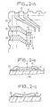
- a housing for example of the "chip carrier” type, marked C c ; it is made up of a base E for example made of ceramic and a cover C A , made of metal or ceramic for example, of which only the trace has been shown on the base E.
- connection pads such as 1 and 2, located at its periphery.
- the base E carries a certain number of conductors in the form of metal deposits such as 21 or 22, which extend to the periphery of the base E.
- the conductive deposits extend in this type of housing inside of half-holes 20, made on the edge of the base, and terminate on the underside of the base where they constitute the outlet connections of the housing.
- connection pads (1,2) of the CE component are connected to the conductors of the base (21,22) by connection wires such as 24. It has also been shown, by way of example, l 'one of the conductors (21) of the base connected to ground.
- the base also carries a component A comprising an element 13 capable of fixing the water molecules.
- component A is a component attached to the base, that is to say that the element 13 is deposited on a substrate 14 on which the entire component is produced. A, this substrate being deposited on the base E. It comprises two connection pads 11 and 12 connected respectively to two of the conductors such as 22 carried by the base, the pads 11 and 12 being connected to a non-visible electrical conductor element in the figure, the function of which is specified below.
- the fixing element 13 can be made of any material capable of fixing water molecules, preferably even when the concentration of these molecules is very low. More specifically, it can be constituted for example by a porous absorbent glass known under the name of "zeolite” or also of "molecular sieve” in the technique of vacuum pumps.
- a treatment degassing
- the fixing element 13 can also be constituted by a material reactive to water, such as a metal alloy, binary or earth for example, one of which at less is reactive to humidity, for example silicon, titanium, zirconium, tantalum, vanadium, aluminum, tin etc .; such an alloy may for example be orsilicon.
- a material reactive to water such as a metal alloy, binary or earth for example, one of which at less is reactive to humidity, for example silicon, titanium, zirconium, tantalum, vanadium, aluminum, tin etc .; such an alloy may for example be orsilicon.
- the fixing of the water is therefore carried out by chemical reaction.
- the resistance connected to the studs 11 and 12 also has the function of heating the element 13 from time to others, after closing the case, in order to allow the atoms of the reactive metal to diffuse towards the surface in contact with the atmosphere of the case, through the oxide layer already formed, renewing the fixing power of the element 13.
- Figure 2a shows a partial top view of an alternative embodiment of the previous figure.
- the base E there is a portion of the base E, the trace of the cover C A , and some conductors such as 22 among which two which are marked 25 and 26.
- the resistance consists of a resistive material marked 15, deposited directly on the base E and partially on the end of the conductors 25 and 26, for example by screen printing; it is covered, after baking, by the material constituting the fixing element 13, which is only visible on the top coming from FIG. 1 or from FIG. 2a, and which can also be deposited by screen printing.
- the resistive material 15 is electrically isolated from the alloy, for example by a thin layer of glass (not shown in the figures).
- a fixing material is used which is at the same time conductive, which avoids the resistive layer 15: in this case, this material, marked 16 , is directly deposited on the base E and the end of the conductors 25 and 26.
- the material 16 can be produced from a resistive material such as a screen printing ink based on Ruthenium oxide, Silver Palladium, Silver Platinum, etc. whose specific surface is increased, thereby producing a porous material capable of fixing the water molecules.
- resistive layer 15 when the fixing element 13 is a metal alloy: it suffices to choose the components of the alloy so as to obtain a resistive compound.
- the component A only requires a single connection 22 left free by the electronic component Ce, the second connection possibly being the ground connection 21.
- Figure 3 shows another embodiment. tion of the housing according to the invention, seen in longitudinal section.
- the housing also includes a cover C A , intended for be sealed on the base E by means of a sealing glass 27.
- the fixing material 13 is carried by the inside of the cover C A where it is deposited for example by screen printing.
- the advantage of this variant compared to the previous ones is twofold.
- the first aspect is that the material 13 can be deposited there in a greater quantity than on the base itself, and the second aspect is the possibility of simply providing energy to the material 13 before sealing the cover C A on the base E.
- this sealing operation requires heating of the cover either in an oven or locally.
- the cover is heated by a tool 30 to a temperature of the order of 500 ° to 650 °, an operation which therefore also causes the heating of the layer 13 and the desired degassing.
- means are provided as above for heating the fixing material to allow the atoms of reactive material to diffuse towards the surface in contact with the atmosphere of the housing.
- the invention is not limited to the embodiments described above.
- a flat chip carrier type housing has been described carrying a single silicon wafer, but the invention is applicable to any flat type or multiple housing (DIL, CERDIP, etc.). levels, whether for discrete component, for integrated circuit or for hybrid circuit, and the term "component" is used in the present application for simplicity, it being understood that it designates any one of these three elements.
- the case described above as being ceramic or metal may be made of plastic, in whole or in part (base or cover).
- the supply of energy necessary for degassing (before closing the casing) of the material fixing the water atoms can be carried out otherwise than by heating, for example by ultra-violet irritation.
Landscapes
- Physics & Mathematics (AREA)
- General Physics & Mathematics (AREA)
- Condensed Matter Physics & Semiconductors (AREA)
- Engineering & Computer Science (AREA)
- Computer Hardware Design (AREA)
- Microelectronics & Electronic Packaging (AREA)
- Power Engineering (AREA)
- Casings For Electric Apparatus (AREA)
- Investigating Or Analyzing Materials By The Use Of Fluid Adsorption Or Reactions (AREA)
Applications Claiming Priority (2)
| Application Number | Priority Date | Filing Date | Title |
|---|---|---|---|
| FR8221871 | 1982-12-28 | ||
| FR8221871A FR2538618B1 (fr) | 1982-12-28 | 1982-12-28 | Boitier pour composant electronique comportant un element fixant l'humidite |
Publications (2)
| Publication Number | Publication Date |
|---|---|
| EP0113282A1 EP0113282A1 (fr) | 1984-07-11 |
| EP0113282B1 true EP0113282B1 (fr) | 1988-02-03 |
Family
ID=9280563
Family Applications (1)
| Application Number | Title | Priority Date | Filing Date |
|---|---|---|---|
| EP83402489A Expired EP0113282B1 (fr) | 1982-12-28 | 1983-12-20 | Boîtier pour composant électronique comportant un élément fixant l'humidité |
Country Status (5)
| Country | Link |
|---|---|
| US (1) | US4553020A (cg-RX-API-DMAC7.html) |
| EP (1) | EP0113282B1 (cg-RX-API-DMAC7.html) |
| JP (1) | JPS59171147A (cg-RX-API-DMAC7.html) |
| DE (1) | DE3375624D1 (cg-RX-API-DMAC7.html) |
| FR (1) | FR2538618B1 (cg-RX-API-DMAC7.html) |
Families Citing this family (35)
| Publication number | Priority date | Publication date | Assignee | Title |
|---|---|---|---|---|
| US4762606A (en) * | 1985-04-12 | 1988-08-09 | Hughes Aircraft Company | Mini chip carrier slotted array |
| IL78192A (en) * | 1985-04-12 | 1992-03-29 | Hughes Aircraft Co | Mini chip carrier slotted array |
| US4802277A (en) * | 1985-04-12 | 1989-02-07 | Hughes Aircraft Company | Method of making a chip carrier slotted array |
| EP0209642A3 (en) * | 1985-07-25 | 1987-04-15 | Hewlett-Packard Company | Ceramic microcircuit package |
| US4777434A (en) * | 1985-10-03 | 1988-10-11 | Amp Incorporated | Microelectronic burn-in system |
| FR2588770B1 (fr) * | 1985-10-22 | 1989-10-27 | Inf Milit Spatiale Aeronaut | Dispositif de limitation de l'humidite dans une enceinte, notamment applicable a un boitier de composant electronique |
| FR2591801B1 (fr) * | 1985-12-17 | 1988-10-14 | Inf Milit Spatiale Aeronaut | Boitier d'encapsulation d'un circuit electronique |
| DE3784213T2 (de) * | 1986-10-29 | 1993-06-03 | Toshiba Kawasaki Kk | Elektronischer apparat mit einem keramischen substrat. |
| GB2233821A (en) * | 1989-07-11 | 1991-01-16 | Oxley Dev Co Ltd | Ceramic package including a semiconductor chip |
| US5166607A (en) * | 1991-05-31 | 1992-11-24 | Vlsi Technology, Inc. | Method and apparatus to heat the surface of a semiconductor die in a device during burn-in while withdrawing heat from device leads |
| US5281852A (en) * | 1991-12-10 | 1994-01-25 | Normington Peter J C | Semiconductor device including stacked die |
| US5397916A (en) * | 1991-12-10 | 1995-03-14 | Normington; Peter J. C. | Semiconductor device including stacked die |
| FR2688629A1 (fr) * | 1992-03-10 | 1993-09-17 | Thomson Csf | Procede et dispositif d'encapsulation en trois dimensions de pastilles semi-conductrices. |
| US5513198A (en) * | 1993-07-14 | 1996-04-30 | Corning Incorporated | Packaging of high power semiconductor lasers |
| FR2709020B1 (fr) * | 1993-08-13 | 1995-09-08 | Thomson Csf | Procédé d'interconnexion de pastilles semi-conductrices en trois dimensions, et composant en résultant. |
| FR2719967B1 (fr) * | 1994-05-10 | 1996-06-07 | Thomson Csf | Interconnexion en trois dimensions de boîtiers de composants électroniques utilisant des circuits imprimés. |
| US5696785A (en) * | 1994-10-11 | 1997-12-09 | Corning Incorporated | Impurity getters in laser enclosures |
| US5837935A (en) * | 1996-02-26 | 1998-11-17 | Ford Motor Company | Hermetic seal for an electronic component having a secondary chamber |
| US5694740A (en) * | 1996-03-15 | 1997-12-09 | Analog Devices, Inc. | Micromachined device packaged to reduce stiction |
| US5709065A (en) * | 1996-07-31 | 1998-01-20 | Empak, Inc. | Desiccant substrate package |
| US6483078B2 (en) | 2000-02-09 | 2002-11-19 | Oceanit Laboratories, Inc. | Moisture control system for electrical devices |
| US6664511B2 (en) * | 2001-07-09 | 2003-12-16 | Jds Uniphase Corporation | Package for optical components |
| FR2832136B1 (fr) * | 2001-11-09 | 2005-02-18 | 3D Plus Sa | Dispositif d'encapsulation hermetique de composant devant etre protege de toute contrainte |
| US6667461B1 (en) * | 2002-06-19 | 2003-12-23 | Tyco Electronics Corporation | Multiple load protection and control device |
| FR2875672B1 (fr) * | 2004-09-21 | 2007-05-11 | 3D Plus Sa Sa | Dispositif electronique avec repartiteur de chaleur integre |
| TW200614854A (en) * | 2004-10-29 | 2006-05-01 | Chunghwa Picture Tubes Ltd | Organic electro-luminescence display panel and fabricating process thereof |
| FR2884049B1 (fr) * | 2005-04-01 | 2007-06-22 | 3D Plus Sa Sa | Module electronique de faible epaisseur comprenant un empilement de boitiers electroniques a billes de connexion |
| FR2894070B1 (fr) * | 2005-11-30 | 2008-04-11 | 3D Plus Sa Sa | Module electronique 3d |
| FR2895568B1 (fr) * | 2005-12-23 | 2008-02-08 | 3D Plus Sa Sa | Procede de fabrication collective de modules electroniques 3d |
| FR2905198B1 (fr) * | 2006-08-22 | 2008-10-17 | 3D Plus Sa Sa | Procede de fabrication collective de modules electroniques 3d |
| FR2923081B1 (fr) * | 2007-10-26 | 2009-12-11 | 3D Plus | Procede d'interconnexion verticale de modules electroniques 3d par des vias. |
| FR2940521B1 (fr) | 2008-12-19 | 2011-11-11 | 3D Plus | Procede de fabrication collective de modules electroniques pour montage en surface |
| FR2943176B1 (fr) | 2009-03-10 | 2011-08-05 | 3D Plus | Procede de positionnement des puces lors de la fabrication d'une plaque reconstituee |
| DE102012200273A1 (de) * | 2012-01-11 | 2013-07-11 | Robert Bosch Gmbh | Elektronisches Bauteil mit korrosionsgeschützter Bondverbindung und Verfahren zur Herstellung des Bauteils |
| EP4177935A1 (en) * | 2021-11-03 | 2023-05-10 | Schott Ag | Hermetic laser-welded enclosure |
Citations (1)
| Publication number | Priority date | Publication date | Assignee | Title |
|---|---|---|---|---|
| DE25647C (de) * | J. GJERS in Middlesbrough on Tees, York (England) | Gemauerte Ausgleichkammern |
Family Cites Families (13)
| Publication number | Priority date | Publication date | Assignee | Title |
|---|---|---|---|---|
| US2127121A (en) * | 1932-09-24 | 1938-08-16 | John E Kelley | Drier for hair and skin |
| US2469435A (en) * | 1944-01-17 | 1949-05-10 | Hirsch Abraham Adler | Regenerable desiccator |
| US2882244A (en) * | 1953-12-24 | 1959-04-14 | Union Carbide Corp | Molecular sieve adsorbents |
| US3304623A (en) * | 1964-07-13 | 1967-02-21 | Realistic Company | Hair dryer |
| US3391517A (en) * | 1966-05-26 | 1968-07-09 | Western Electric Co | Methods and apparatus for seating nonmagnetic articles in paramagnetic containers |
| US3586926A (en) * | 1967-11-30 | 1971-06-22 | Nippon Electric Co | Hermetically sealed semiconductor device with absorptive agent |
| GB1501878A (en) * | 1975-09-09 | 1978-02-22 | Thorn Electrical Ind Ltd | Electroluminescent panel |
| DE2744146C3 (de) * | 1977-09-30 | 1982-03-11 | Heimann Gmbh, 6200 Wiesbaden | Regelbare Wasserstoffquelle mit Getterwirkung zum Einbau in Elektronenröhren, insbesondere Vidikonröhren |
| US4357557A (en) * | 1979-03-16 | 1982-11-02 | Sharp Kabushiki Kaisha | Glass sealed thin-film electroluminescent display panel free of moisture and the fabrication method thereof |
| JPS5635383A (en) * | 1979-08-29 | 1981-04-08 | Kyoto Ceramic | Semiconductor integrated circuit support with heating mechanism |
| US4352119A (en) * | 1979-09-17 | 1982-09-28 | Beckman Instruments, Inc. | Electrical device and method for particle entrapment device for an electrical component |
| JPS56137658A (en) * | 1980-03-31 | 1981-10-27 | Chiyou Lsi Gijutsu Kenkyu Kumiai | Semiconductor device |
| US4426769A (en) * | 1981-08-14 | 1984-01-24 | Amp Incorporated | Moisture getter for integrated circuit packages |
-
1982
- 1982-12-28 FR FR8221871A patent/FR2538618B1/fr not_active Expired
-
1983
- 1983-12-20 DE DE8383402489T patent/DE3375624D1/de not_active Expired
- 1983-12-20 EP EP83402489A patent/EP0113282B1/fr not_active Expired
- 1983-12-23 US US06/565,042 patent/US4553020A/en not_active Expired - Fee Related
- 1983-12-28 JP JP58245634A patent/JPS59171147A/ja active Granted
Patent Citations (1)
| Publication number | Priority date | Publication date | Assignee | Title |
|---|---|---|---|---|
| DE25647C (de) * | J. GJERS in Middlesbrough on Tees, York (England) | Gemauerte Ausgleichkammern |
Also Published As
| Publication number | Publication date |
|---|---|
| EP0113282A1 (fr) | 1984-07-11 |
| JPH0322702B2 (cg-RX-API-DMAC7.html) | 1991-03-27 |
| JPS59171147A (ja) | 1984-09-27 |
| US4553020A (en) | 1985-11-12 |
| FR2538618B1 (fr) | 1986-03-07 |
| FR2538618A1 (fr) | 1984-06-29 |
| DE3375624D1 (en) | 1988-03-10 |
Similar Documents
| Publication | Publication Date | Title |
|---|---|---|
| EP0113282B1 (fr) | Boîtier pour composant électronique comportant un élément fixant l'humidité | |
| TWI317180B (en) | Optoelectronic component, device with several optoelectronic components and method to produce an optoelectronic component | |
| KR101620113B1 (ko) | 광전 소자 및 광전 소자 제조 방법 | |
| CN1139293A (zh) | 有机器件的钝化 | |
| FR2700416A1 (fr) | Dispositif à semiconducteurs comportant un élément semiconducteur sur un élément de montage. | |
| FR2591801A1 (fr) | Boitier d'encapsulation d'un circuit electronique | |
| US8866181B2 (en) | Method for producing a component with at least one organic material and component with at least one organic material | |
| KR20000023055A (ko) | 발광 소자 및 그 접점 패턴화 방법 | |
| FR2604029A1 (fr) | Puce de circuit integre possedant des bornes de sortie ameliorees | |
| US20090140282A1 (en) | Led structure for flip-chip package and method thereof | |
| DE3161228D1 (en) | Gold metallisation in semiconductor devices | |
| FR2518811A1 (fr) | Dispositif a circuit integre en conteneur de ceramique | |
| EP2212924B1 (fr) | Perfectionnements apportés à un boîtier de connexion pour éléments capables de collecter de la lumière | |
| FR2956521A1 (fr) | Dispositif comprenant des composants electriques, electroniques, electromecaniques ou electro-optiques, a sensibilite reduite a faible debit de dose | |
| FR2829874A1 (fr) | Systeme a semi-conducteur a boitier et enveloppe | |
| EP0135230B1 (fr) | Dispositif semi-conducteur, notamment transistor incluant des moyens de protection contre les surcharges | |
| EP0018890B1 (fr) | Support isolateur électrique, à faible résistance thermique, et embase ou boîtier pour composant de puissance comportant un tel support | |
| CN105308762A (zh) | 利用ald层封装的光电子半导体芯片和相应的制造方法 | |
| KR20110126655A (ko) | 전장 발광 장치 | |
| FR2880117A1 (fr) | Detecteur de pression resistant aux acides | |
| FR2528655A1 (fr) | Ballast pour lampe a incandescence basse tension et lampe ainsi obtenue | |
| FR2588770A1 (fr) | Dispositif de limitation de l'humidite dans une enceinte, notamment applicable a un boitier de composant electronique | |
| FR2620275A1 (fr) | Boitier pour le montage en surface d'un composant fonctionnant en hyperfrequences | |
| FR3012204A1 (fr) | Systeme de connexion electrique d'au moins une source de lumiere a un systeme d'alimentation electrique | |
| FR2538170A1 (fr) | Circuit de relais de courant alternatif a semi-conducteurs et structure de thyristor associee |
Legal Events
| Date | Code | Title | Description |
|---|---|---|---|
| PUAI | Public reference made under article 153(3) epc to a published international application that has entered the european phase |
Free format text: ORIGINAL CODE: 0009012 |
|
| AK | Designated contracting states |
Designated state(s): DE GB IT NL SE |
|
| 17P | Request for examination filed |
Effective date: 19841205 |
|
| 17Q | First examination report despatched |
Effective date: 19860619 |
|
| RAP1 | Party data changed (applicant data changed or rights of an application transferred) |
Owner name: THOMSON-CSF |
|
| GRAA | (expected) grant |
Free format text: ORIGINAL CODE: 0009210 |
|
| AK | Designated contracting states |
Kind code of ref document: B1 Designated state(s): DE IT |
|
| ITF | It: translation for a ep patent filed | ||
| REF | Corresponds to: |
Ref document number: 3375624 Country of ref document: DE Date of ref document: 19880310 |
|
| PLBE | No opposition filed within time limit |
Free format text: ORIGINAL CODE: 0009261 |
|
| STAA | Information on the status of an ep patent application or granted ep patent |
Free format text: STATUS: NO OPPOSITION FILED WITHIN TIME LIMIT |
|
| 26N | No opposition filed | ||
| PGFP | Annual fee paid to national office [announced via postgrant information from national office to epo] |
Ref country code: DE Payment date: 19921112 Year of fee payment: 10 |
|
| ITTA | It: last paid annual fee | ||
| PG25 | Lapsed in a contracting state [announced via postgrant information from national office to epo] |
Ref country code: DE Effective date: 19940901 |