EP0113232A2 - Système de traitement d'erreur de machine - Google Patents
Système de traitement d'erreur de machine Download PDFInfo
- Publication number
- EP0113232A2 EP0113232A2 EP83307770A EP83307770A EP0113232A2 EP 0113232 A2 EP0113232 A2 EP 0113232A2 EP 83307770 A EP83307770 A EP 83307770A EP 83307770 A EP83307770 A EP 83307770A EP 0113232 A2 EP0113232 A2 EP 0113232A2
- Authority
- EP
- European Patent Office
- Prior art keywords
- error
- error data
- machine check
- processing unit
- saving
- Prior art date
- Legal status (The legal status is an assumption and is not a legal conclusion. Google has not performed a legal analysis and makes no representation as to the accuracy of the status listed.)
- Granted
Links
Images
Classifications
-
- G—PHYSICS
- G06—COMPUTING OR CALCULATING; COUNTING
- G06F—ELECTRIC DIGITAL DATA PROCESSING
- G06F11/00—Error detection; Error correction; Monitoring
-
- G—PHYSICS
- G06—COMPUTING OR CALCULATING; COUNTING
- G06F—ELECTRIC DIGITAL DATA PROCESSING
- G06F11/00—Error detection; Error correction; Monitoring
- G06F11/22—Detection or location of defective computer hardware by testing during standby operation or during idle time, e.g. start-up testing
- G06F11/2205—Detection or location of defective computer hardware by testing during standby operation or during idle time, e.g. start-up testing using arrangements specific to the hardware being tested
-
- G—PHYSICS
- G06—COMPUTING OR CALCULATING; COUNTING
- G06F—ELECTRIC DIGITAL DATA PROCESSING
- G06F11/00—Error detection; Error correction; Monitoring
- G06F11/30—Monitoring
- G06F11/34—Recording or statistical evaluation of computer activity, e.g. of down time, of input/output operation ; Recording or statistical evaluation of user activity, e.g. usability assessment
Definitions
- the present invention relates to a machine check processing system. More particularly, it relates to a system having an error correcting function, wherein error data relating to a corrected error can be saved by a service processing unit (SVP).
- SVP service processing unit
- a known data processing system has a main memory, a memory control unit (MCU), a central processing unit (CPU), and an SVP.
- a correctable error for example, a single bit error occurs during data processing
- the error is corrected in the MCU.
- a predetermined area in the main memory is informed of data relating to the error, for example, the place where the single bit error occurred.
- This storing of error data is carried out for the purpose of knowing the site of the single bit error. That is, if the single bit error is a hard error, the possibility of an uncorrectable error, i.e., a double bit error, occurring is high. Therefore, an operator, a user, or a maintenance man needs to know the place where a single bit error occurs.
- the predetermined area in the main memory is not a large area, it cannot store many pieces of error data. Therefore, the error data must be saved in another place or must be output to an outer device everytime the predetermined area is full of error data. This saving or outputting process is very troublesome for the user.
- a machine check interruption occurs on every occasion on which error data is stored in the predetermined area in the main memory so that data processing is interrupted during that period.
- the predetermined area in the main memory is not informed of any subsequent error data so that machine check interruption due to a single bit error no longer occurs.
- An / of the present invention can provide a machine check processing system in which error data relating to a corrected error can be automatically saved and analyzed by an SVP without substantially interrupting the system processing.
- the SVP can inhibit subsequent machine
- An embodiment of the present invention can also provide such a machine check processing system as above, wherein a maintenance man, etc. can obtain error data even after machine check interruption due to a single bit error is inhibited.
- a machine check processing system comprising: an error correcting means for correcting a correctable error generated during data processing; an error data storing means for storing error data which relates to the correctable error; a CPU for controlling the error correcting means and the error data storing means; and an SVP for operating and controlling the error correcting means, the error data storing means, and the CPU.
- the CPU comprises an error data freezing means for freezing (securing)data stored in the error data storing means when a correctable error occurs and a machine check record request signal generating means for generating a machine check record request signal when a correctable error occurs.
- the SVP comprises an error data saving means for carrying out a saving process so as to save the frozen error data stored in the error data storing means in response to the machine check record request signal, an error data analyzing means for carrying out an error analyzing process, and a freeze release means for releasing the error data stored in the error data storing means from a frozen state after the error data saving means saves the error data, whereby at least a part of the saving process and the error analyzing process are carried out substantially simultaneous with the operation of the CPU.
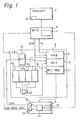
- Figure 1 shows a machine check processing system ' according to an embodiment of the present invention.
- reference numeral 1 designates a main memory 1, 2 an MCU, 3 a CPU, 4 an SVP including a system console, 5 an error data freezing circuit (FRE), 6 a machine check interruption circuit (MCK), 7 a machine check record request signal generating circuit (REC REQ), 8 an inhibiting flip-flop for inhibiting a machine check interruption, 9 1 through 9 4 error flip-flops for latching errors in the main memory, the CPU, or other places, 10 an OR circuit, 11 a failing storage address register (FSAR) for storing error data relating to a corrected error, 12 a fixed area in the main memory 1, 13 a floppy disk for saving the error data from FSAR 11, 14 an error data analyzing circuit, 15 a freeze release circuit, and 16 a CPU mode changing circuit.
- FRE error data freezing circuit
- MK machine check interruption circuit
- REC REQ machine check record request signal generating circuit
- 8 an inhibiting flip-flop for inhibiting
- the CPU 3 accesses the main memory 1 through the MCU 2 to execute instructions.
- a correctable error i.e., a single bit error
- the MCU 2 corrects the single bit error, stores in the FSAR 11 error data such as the site of the single bit error, and sends an error informing signal (EIS) to the FRE 5 and to one of the error flip-flops 9 1 through 9 4 .
- EIS error informing signal
- the error flip-flops 9 1 through 9 4 respectively, correspond to the main memory 1, the CPU 3, and other places.For example, if the single bit error occurs in the main memory 1, the EIS is received by the flip-flop 9 1 .
- the error data freezing circuit 5 when it receives the EIS, sends a freezing signal (FS) to the FSAR 11 so that the error data stored in the FSAR 11 is frozen at a time t l .
- FS freezing signal
- the error flip-flop 9 1 when it receives the EIS, provides a trigger through the OR circuit 10 to the MCK 6 and REC REQ 7 at a time t 2 .
- the fixed area 12 is large, the remaining area in the main memory 1 used for data processing is limited. Therefore, the fixed area 12 should not be large, and, usually, it can store only one piece of error data relating to a single bit error.
- a maintenance man can obtain error data only when he reads the contents of the fixed area 12 of the main memory every time the fixed area 12 is full of error data. This reading is troublesome.
- This process for error storage may be considered to be unnecessary in the present invention.
- a maintenance man, etc. may handle a single bit error in the conventional way or in the way according to the present invention. Therefore, it is preferable to provide a machine check interruption process for outputting the contents stored in the FSAR 11 to the fixed area 12.
- the REC REQ 7 when it receives the trigger from the error flip-flop 91 for example, provides a machine check record request signal (MCK REC REQ) to the SVP 4 at a time t 3 .
- MCK REC REQ machine check record request signal
- the SVP 4 receives the MCK REC REQ from the REC REQ 7, the floppy disk 13 in the SVP 4 starts to save the error data frozen in the FSAR 11 in the MCU 2 at the time t 3 .
- the CPU again starts a normal system operation subsequent to the operation in which the single bit error occurred.
- the error data analyzing circuit 14 starts to analyze the error data saved in the floppy disk 13 at a time t 5 . It should be noted that the error data analyzing process and part of the saving process are automatically carried out simultaneous with the above-mentioned subsequent system operation by the CPU 3 unless a system down status is assumed. As a result of error data analysis, if the error is recognized as being a kind of error that does not necessitate a machine check interruption, the error data analyzing circuit 14 drives the CPU mode changing circuit 16 so that it provides an inhibit signal to the inhibiting flip-flop 8 in the CPU 3. For example, if the analyzed error data indicates that the site of the error is the same as the site of the previously saved error, the error is recognized as being a hard error.
- the inhibiting flip--flop 8 when it receives the inhibit signal from the circuit 16, provides an inhibit signal to the machine check interruption circuit 6 at a time t 6 so that, after the time t 6 , machine check interruption is inhibited.
- the mode of the CPU 3 is changed from a state where a machine check interruption occurs every time a single bit error is detected to a state where no machine check interruption occurs even when a single bit error is detected.
- the error analyzing circuit 14 drives the freeze release circuit 15 so that it sends a log save end signal to the error flip-flops 9 1 through 9 4 , to the REC REQ 7, and to the error data freezing circuit 5 in the CPU 3 so as to reset them at a time t 7 .
- the outputs of the FRE 5, the REC REQ 7, and the inhibiting flip-flop 8 are turned off so that the error data stored in the FSAR 11 is unfrozen.
- inhibition of machine check interruption is effected when the site of the corrected error is the same as the site of the previously corrected error.
- the present invention is not limited to the above case. According to the operator's requirement, any condition as the result of error analysis may cause inhibition of machine check interruption.
- a machine check interruption may occur every time a predetermined number when of single bit errors are detected instead of/only a single bit error is detected.
- an improved machine check processing system is obtained in which error data relating to a corrected error can be automatically saved and analyzed by an SVP without substantially interrupting the system processing. Further, the SV P can change the mode of the CPU from a state where a machine check interruption occurs everytime a single bit error is detected,to a state where no machine check interruption occurs even when a single bit error is detected.
Landscapes
- Engineering & Computer Science (AREA)
- Theoretical Computer Science (AREA)
- General Engineering & Computer Science (AREA)
- Quality & Reliability (AREA)
- Physics & Mathematics (AREA)
- General Physics & Mathematics (AREA)
- Computer Hardware Design (AREA)
- Debugging And Monitoring (AREA)
- Techniques For Improving Reliability Of Storages (AREA)
- Detection And Correction Of Errors (AREA)
Applications Claiming Priority (2)
| Application Number | Priority Date | Filing Date | Title |
|---|---|---|---|
| JP229290/82 | 1982-12-29 | ||
| JP57229290A JPS59123058A (ja) | 1982-12-29 | 1982-12-29 | マシンチエツク処理方式 |
Publications (3)
| Publication Number | Publication Date |
|---|---|
| EP0113232A2 true EP0113232A2 (fr) | 1984-07-11 |
| EP0113232A3 EP0113232A3 (en) | 1986-07-02 |
| EP0113232B1 EP0113232B1 (fr) | 1988-10-12 |
Family
ID=16889802
Family Applications (1)
| Application Number | Title | Priority Date | Filing Date |
|---|---|---|---|
| EP83307770A Expired EP0113232B1 (fr) | 1982-12-29 | 1983-12-20 | Système de traitement d'erreur de machine |
Country Status (8)
| Country | Link |
|---|---|
| US (1) | US4593391A (fr) |
| EP (1) | EP0113232B1 (fr) |
| JP (1) | JPS59123058A (fr) |
| KR (1) | KR890002285B1 (fr) |
| BR (1) | BR8307228A (fr) |
| CA (1) | CA1203915A (fr) |
| DE (1) | DE3378235D1 (fr) |
| ES (1) | ES528476A0 (fr) |
Cited By (3)
| Publication number | Priority date | Publication date | Assignee | Title |
|---|---|---|---|---|
| EP0218979A3 (en) * | 1985-10-03 | 1988-08-31 | Mitsubishi Denki Kabushiki Kaisha | Computer program debugging system |
| EP0380858A3 (fr) * | 1989-02-03 | 1991-08-28 | Digital Equipment Corporation | Procédé et dispositif de détection et de correction d'erreur dans un système de calculateur à pipeline |
| EP0618549A1 (fr) * | 1993-03-25 | 1994-10-05 | Siemens Aktiengesellschaft | Procédé de surveillance pour un appareil électrique |
Families Citing this family (16)
| Publication number | Priority date | Publication date | Assignee | Title |
|---|---|---|---|---|
| US5097413A (en) * | 1983-09-20 | 1992-03-17 | Mensch Jr William D | Abort circuitry for microprocessor |
| JPS6134793A (ja) * | 1984-07-27 | 1986-02-19 | Hitachi Ltd | ダイナミツクメモリ装置における診断及びエラ−訂正装置 |
| US4679195A (en) * | 1985-04-10 | 1987-07-07 | Amdahl Corporation | Error tracking apparatus in a data processing system |
| US4752928A (en) * | 1985-05-06 | 1988-06-21 | Tektronix, Inc. | Transaction analyzer |
| JPH0792773B2 (ja) * | 1986-02-07 | 1995-10-09 | 三洋電機株式会社 | 故障検知方法 |
| US5278840A (en) * | 1987-07-01 | 1994-01-11 | Digital Equipment Corporation | Apparatus and method for data induced condition signalling |
| US5121475A (en) * | 1988-04-08 | 1992-06-09 | International Business Machines Inc. | Methods of dynamically generating user messages utilizing error log data with a computer system |
| JPH02297228A (ja) * | 1989-05-11 | 1990-12-07 | Fujitsu Ltd | 障害情報格納方式 |
| US5448725A (en) * | 1991-07-25 | 1995-09-05 | International Business Machines Corporation | Apparatus and method for error detection and fault isolation |
| US5307482A (en) * | 1992-01-28 | 1994-04-26 | International Business Machines Corp. | Computer, non-maskable interrupt trace routine override |
| US5305197A (en) * | 1992-10-30 | 1994-04-19 | Ie&E Industries, Inc. | Coupon dispensing machine with feedback |
| US5418794A (en) * | 1992-12-18 | 1995-05-23 | Amdahl Corporation | Error determination scan tree apparatus and method |
| FI102220B1 (fi) * | 1995-10-30 | 1998-10-30 | Nokia Telecommunications Oy | Vikaantumistietojen keräys tietokoneyksikön uudelleenkäynnistyksen osana |
| US7315961B2 (en) * | 2002-06-27 | 2008-01-01 | Intel Corporation | Black box recorder using machine check architecture in system management mode |
| US7243174B2 (en) * | 2003-06-24 | 2007-07-10 | Emerson Electric Co. | System and method for communicating with an appliance through an optical interface using a control panel indicator |
| US10318368B2 (en) * | 2016-05-31 | 2019-06-11 | Intel Corporation | Enabling error status and reporting in a machine check architecture |
Family Cites Families (9)
| Publication number | Priority date | Publication date | Assignee | Title |
|---|---|---|---|---|
| US3999051A (en) * | 1974-07-05 | 1976-12-21 | Sperry Rand Corporation | Error logging in semiconductor storage units |
| US4315311A (en) * | 1975-10-28 | 1982-02-09 | Compagnie Internationale Pour L'informatique Cii-Honeywell Bull (Societe Anonyme) | Diagnostic system for a data processing system |
| US4212059A (en) * | 1977-03-14 | 1980-07-08 | Tokyo Shibaura Electric Co., Ltd. | Information processing system |
| US4355389A (en) * | 1977-03-15 | 1982-10-19 | Tokyo Shibaura Electric Co., Ltd. | Microprogrammed information processing system having self-checking function |
| JPS54121036A (en) * | 1978-03-13 | 1979-09-19 | Cho Lsi Gijutsu Kenkyu Kumiai | Method of testing function of logic circuit |
| US4506362A (en) * | 1978-12-22 | 1985-03-19 | Gould Inc. | Systematic memory error detection and correction apparatus and method |
| JPS56110163A (en) * | 1980-02-06 | 1981-09-01 | Hitachi Ltd | Logout system |
| US4463418A (en) * | 1981-06-30 | 1984-07-31 | International Business Machines Corporation | Error correction from remote data processor by communication and reconstruction of processor status storage disk |
| JPS58181550A (ja) * | 1982-04-13 | 1983-10-24 | Tatsuo Okazaki | 刃物の砥ぎ具 |
-
1982
- 1982-12-29 JP JP57229290A patent/JPS59123058A/ja active Granted
-
1983
- 1983-12-15 CA CA000443403A patent/CA1203915A/fr not_active Expired
- 1983-12-20 EP EP83307770A patent/EP0113232B1/fr not_active Expired
- 1983-12-20 DE DE8383307770T patent/DE3378235D1/de not_active Expired
- 1983-12-20 US US06/563,654 patent/US4593391A/en not_active Expired - Lifetime
- 1983-12-23 KR KR1019830006134A patent/KR890002285B1/ko not_active Expired
- 1983-12-28 ES ES528476A patent/ES528476A0/es active Granted
- 1983-12-28 BR BR8307228A patent/BR8307228A/pt not_active IP Right Cessation
Cited By (3)
| Publication number | Priority date | Publication date | Assignee | Title |
|---|---|---|---|---|
| EP0218979A3 (en) * | 1985-10-03 | 1988-08-31 | Mitsubishi Denki Kabushiki Kaisha | Computer program debugging system |
| EP0380858A3 (fr) * | 1989-02-03 | 1991-08-28 | Digital Equipment Corporation | Procédé et dispositif de détection et de correction d'erreur dans un système de calculateur à pipeline |
| EP0618549A1 (fr) * | 1993-03-25 | 1994-10-05 | Siemens Aktiengesellschaft | Procédé de surveillance pour un appareil électrique |
Also Published As
| Publication number | Publication date |
|---|---|
| ES8501901A1 (es) | 1984-12-01 |
| EP0113232A3 (en) | 1986-07-02 |
| JPS6363933B2 (fr) | 1988-12-09 |
| KR840007189A (ko) | 1984-12-05 |
| KR890002285B1 (ko) | 1989-06-27 |
| DE3378235D1 (en) | 1988-11-17 |
| ES528476A0 (es) | 1984-12-01 |
| CA1203915A (fr) | 1986-04-29 |
| US4593391A (en) | 1986-06-03 |
| EP0113232B1 (fr) | 1988-10-12 |
| BR8307228A (pt) | 1984-08-07 |
| JPS59123058A (ja) | 1984-07-16 |
Similar Documents
| Publication | Publication Date | Title |
|---|---|---|
| EP0113232B1 (fr) | Système de traitement d'erreur de machine | |
| US6502206B1 (en) | Multi-processor switch and main processor switching method | |
| US4491914A (en) | Initial program load system | |
| US6233693B1 (en) | Smart DASD spin-up | |
| US5442777A (en) | Firmware trace data acquisition method | |
| US4839895A (en) | Early failure detection system for multiprocessor system | |
| US5630044A (en) | Memory fault recovery system which executes degradation or recovery of memory | |
| US7032019B1 (en) | Apparatuses for generation and collection of information based on priority and predetermined collecting conditions | |
| US7752496B2 (en) | Method, apparatus, and computer product for managing log data | |
| US6026504A (en) | Multiprocessor system and method for error tracking | |
| US6907303B2 (en) | Switching circuit for board duplication apparatus | |
| JPH0786841B2 (ja) | 障害情報ログ方法及びデータ処理装置 | |
| JP2508305B2 (ja) | 初期値決定装置 | |
| CN120723188B (zh) | 一种调试信息的打印方法、电子设备 | |
| JP2870202B2 (ja) | プロセッサ間相互監視方法及びその装置 | |
| JPH02281343A (ja) | Cpu動作の監視方式 | |
| JPS6310463B2 (fr) | ||
| JP2002073375A (ja) | マイクロコンピュータを有するシステムにおけるソフトウェアの動作監視方法 | |
| JP2681005B2 (ja) | パッケージ実装変化監視機能を有する制御装置 | |
| JP3757407B2 (ja) | 制御装置 | |
| US4587654A (en) | System for processing machine check interruption | |
| JP2676609B2 (ja) | データ伝送方式 | |
| JPH04175838A (ja) | オートリブート時のダンプ方式 | |
| JPS63123140A (ja) | 履歴情報記憶装置 | |
| JPH07306811A (ja) | メモリ故障診断方法 |
Legal Events
| Date | Code | Title | Description |
|---|---|---|---|
| PUAI | Public reference made under article 153(3) epc to a published international application that has entered the european phase |
Free format text: ORIGINAL CODE: 0009012 |
|
| AK | Designated contracting states |
Designated state(s): DE FR GB |
|
| PUAL | Search report despatched |
Free format text: ORIGINAL CODE: 0009013 |
|
| AK | Designated contracting states |
Kind code of ref document: A3 Designated state(s): DE FR GB |
|
| 17P | Request for examination filed |
Effective date: 19860729 |
|
| 17Q | First examination report despatched |
Effective date: 19870804 |
|
| GRAA | (expected) grant |
Free format text: ORIGINAL CODE: 0009210 |
|
| AK | Designated contracting states |
Kind code of ref document: B1 Designated state(s): DE FR GB |
|
| REF | Corresponds to: |
Ref document number: 3378235 Country of ref document: DE Date of ref document: 19881117 |
|
| ET | Fr: translation filed | ||
| PLBE | No opposition filed within time limit |
Free format text: ORIGINAL CODE: 0009261 |
|
| STAA | Information on the status of an ep patent application or granted ep patent |
Free format text: STATUS: NO OPPOSITION FILED WITHIN TIME LIMIT |
|
| 26N | No opposition filed | ||
| PGFP | Annual fee paid to national office [announced via postgrant information from national office to epo] |
Ref country code: FR Payment date: 19991208 Year of fee payment: 17 |
|
| PGFP | Annual fee paid to national office [announced via postgrant information from national office to epo] |
Ref country code: GB Payment date: 19991215 Year of fee payment: 17 |
|
| PGFP | Annual fee paid to national office [announced via postgrant information from national office to epo] |
Ref country code: DE Payment date: 19991220 Year of fee payment: 17 |
|
| PG25 | Lapsed in a contracting state [announced via postgrant information from national office to epo] |
Ref country code: GB Free format text: LAPSE BECAUSE OF NON-PAYMENT OF DUE FEES Effective date: 20001220 |
|
| GBPC | Gb: european patent ceased through non-payment of renewal fee |
Effective date: 20001220 |
|
| PG25 | Lapsed in a contracting state [announced via postgrant information from national office to epo] |
Ref country code: FR Free format text: LAPSE BECAUSE OF NON-PAYMENT OF DUE FEES Effective date: 20010831 |
|
| REG | Reference to a national code |
Ref country code: FR Ref legal event code: ST |
|
| PG25 | Lapsed in a contracting state [announced via postgrant information from national office to epo] |
Ref country code: DE Free format text: LAPSE BECAUSE OF NON-PAYMENT OF DUE FEES Effective date: 20011002 |